DOI:
10.1039/D2RA01156E
(Paper)
RSC Adv., 2022,
12, 15814-15821
High-performance ferroelectric nonvolatile memory based on Gd-and Ni-codoped BiFeO3 films
Received
21st February 2022
, Accepted 3rd May 2022
First published on 25th May 2022
Abstract
BiFeO3 (BFO), Bi0.92Gd0.08FeO3 (BGFO) and Bi0.92Gd0.08Fe0.95Ni0.05O3 (BGFNO) films are epitaxially grown on 0.7 wt% Nb-SrTiO3 (NSTO) substrates. The strong ferroelectric property in BGFNO film is confirmed by piezoresponse force microscopy (PFM) and polarization versus voltage (P–V) measurement. It is also found that the Au/BGFNO/NSTO devices possess a ferroelectric resistance switching (RS) effect. Gd- and Ni-codoped BiFeO3 is found to strongly enhance the resistance on/off ratio. A resistance on/off ratio as large as 3 × 10⁶ is achieved with an applied pulse voltage of −8 V and +4 V. In addition, the devices exhibit excellent retention and anti-fatigue characteristics. The memristor behavior of Au/BGFNO/NSTO is attributed to the switching of polarization states, which modulate the width and height of the barrier at the BGFNO/NSTO interface. The excellent resistive switching properties in Au/BGFNO/NSTO devices indicate the promising application in nonvolatile memory.
Introduction
In recent years, resistive random access memory (RRAM) has become the focus of research in the field of ferroelectric memory because of the advantages such as simple structure, high storage density, low power consumption, fast access speed and non-volatile properties. It has been proved that ferroelectric resistance memory based on a ferroelectric diode and tunnel junction can achieve a high resistance on/off ratio, high speed, low write power and high reproducibility by controlling ferroelectric polarization. BiFeO3, as a typical ABO3 perovskite material, has been extensively studied in photovoltaic, photoelectric and magnetoelectric coupling effects, which makes BiFeO3 a potential candidate to realize multifunctional devices.1–6 However, BiFeO3 thin films have many oxygen vacancies and a large leakage current density, the ferroelectric polarization is quite small at room temperature, which is due to the volatilization of Bi and change in the valence state of Fe. It is well known that ion doping affects the structure, ferroelectric properties, and charge transport properties of the film.7,8 When rare earth ions such as lanthanide ions are substituted at bismuth site, the leakage current and the dielectric loss of BiFeO3 films reduces.9,10 The formation of oxygen vacancy and the fluctuation of Fe ion valence can be inhibited by doping at site B.11,12 And transition metal doping replaces iron site to modify g-type antiferromagnetic structure, which is an effective method to enhance ferromagnetic order degree of BiFeO3 widely used at present.11,13–15 For example, Pranab Parimal Biswas et al. enhanced Voc (open-circuit voltage) of photovoltaic devices by La doping at site A.16 Fen Liu et al. improved the fatigue resistance of BiFeO3 films by Co doping.17 In addition, G. D. Hu et al. reported that Gd doping can significantly reduce the leakage current and improve the Pr (remanent polarization) value of BiFeO3 films, and the films exhibits almost no loss of the Pr value after 109 cycles.18 Deng et al. found that nickel doping is an effective way to enhance Mr Value of BiFeO3 films.11 By co-doping at site A and B, the advantages of two or more ions can be combined to reduce the dielectric loss, enhance Pr and Mr (remanent magnetization) value of BiFeO3 films.10,14,15,19 Gd and Ni co-doped BiFeO3 film has lower leakage current density, higher Pr and Mr value.8,20 However, the research on resistance switching (RS) properties in co-doped BiFeO3 films is limited. In this paper, the bipolar RS effects of BiFeO3 doped with 8% Gd and 5% Ni (BGFNO) in the Au/BGFNO/NSTO heterojunction were reported. The resistance changed with the write pulse voltage amplitude, and the resistance was continuously adjustable. Moreover, the remanent polarization was greatly improved. The BGFNO film exhibited large on/off ratio, good retention and fatigue resistance, in which the memory behavior was attributed to the ferroelectric polarization modulation at the BGFNO/NSTO interface.
Experimental procedure
The commercial (001) single-crystal Nb-doped STO (Nb: 0.7 wt%) (NSTO) substrates were successively cleaned in 15 min with ethanol, acetone, and de-ionized water and then blown with air before deposition. The BiFeO3 (BFO), Bi0.92Gd0.08FeO3 (BGFO) and Bi0.92Gd0.08Fe0.95Ni0.05O3 (BGFNO) films (∼60 nm) were epitaxially grown on the NSTO substrates using pulsed laser deposition (PLD) with a KrF excimer laser wavelength of 248 nm at a frequency of 2 Hz, in which the laser fluence was 1.5 J cm−2 with a spot area of 7.5 mm2 on the target, and the target–substrate distance was set at 6.5 cm. The deposition was performed under an oxygen partial pressure of 0.1 Torr at a substrate temperature of 630 °C for 30 min. After deposition, the samples were annealed in situ for 30 min and then cooled to room temperature at 5 °C min−1. The structure of the three films grown on the NSTO substrates was analyzed by X-ray diffraction (XRD, DX-2700) with a Cu X-ray source (λ = 1.5406 Å). The film thicknesses were characterized using a scanning electron microscope (SEM, JSM-7001F). The nanoscale resolution topography, ferroelectric switching properties, conduction properties, and surface potential of the samples were provided via atomic force microscopy (AFM), piezoelectric force microscopy (PFM), conductive atomic force microscopy (CAFM), and Kelvin probe force microscopy (KPFM) using an Asylum Research 3D Infinity instrument with a conductive tip (TiIr Coating). Au top electrodes with area of 4 × 10⁻⁴ cm2 were deposited by DC magnetron sputtering to form Au/BFO/NSTO heterostructure, and the in bottom electrode was smeared onto the back of NSTO substrate to ensure ohmic contact during the electrical measurements. The resistance switching of the three devices were measured using a Keithley 2400 Source-Meter, the voltage pulse was supplied by using an arbitrary wave form generator (Agilent 33250A), and the NSTO substrate was grounded through an indium ohmic contact pad. During the measurement, the forward bias was defined as a positive DC voltage applied on the Au top electrodes. The measure of P–V loops was performed via a semiconductor device analyzer (WGMFMU, B1500A). All measurements were carried out at room temperature.
Results
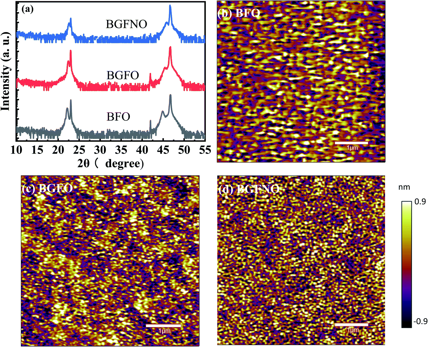
The θ–2θ scan in Fig. 1(a) only shows (001) and (002) diffraction peaks of the BFO, BGFO, and BGFNO films, which indicates uniformly c-axis orientation without any impurity phase within resolution. The surface morphology of the BFO/NSTO, BGFO/NSTO and BGFNO/NSTO heterostructure are examined to assess the quality of the films, as shown in Fig. 1(b–d). The three films have an atomically smooth surfaces, and the square root roughness of BFO, BGFO and BGFNO is 1.13 nm and 1.27 nm and 0.81 nm in an area of 5 × 5 μm2, respectively. The low square root roughness of the BGFNO films confirms the excellent quality of the films.
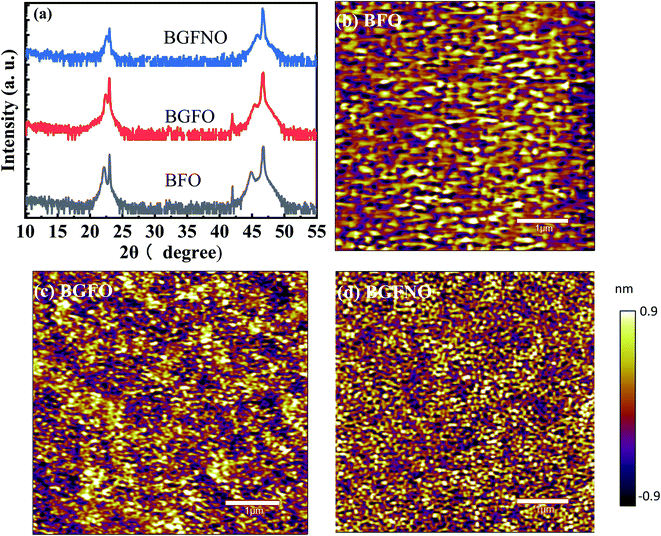 |
| | Fig. 1 (a) XRD θ–2θ scan of BFO, BGFO, and BGFNO. Surface morphology of 60 nm-thick (b) BFO (c) BGFO and (d) BGFNO layer grown on the NSTO substrate. | |
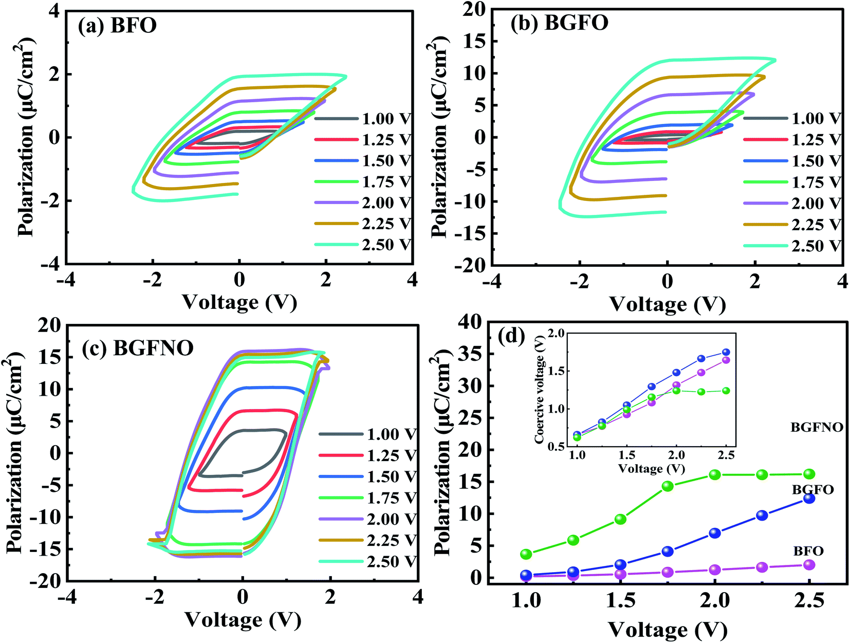
Fig. 2(a–c) shows the P–V loops of the BFO, BGFO and BGFNO films at 10 kHz under various applied voltages, which further illustrates the robust ferroelectricity of the BGFNO films. Dependence of remanent polarization and coercive voltage [inset of (d)] on the applied voltage are shown in Fig. 2(d). A clear increasing trend for Pr and coercive voltage with applied voltage is observed in BFO and BGFO films, which shows that the Pr of BGFNO film higher than that of the BFO and BGFO, which implies that Gd and Ni co-doping can effectively improve the Pr value of BFO. In addition, it can be seen the P–V loops of BFO and BGFO films are not saturated, whereas the P–V loop of BGFNO film is saturated at the applied voltage of 2 V, which may be due to the smaller grain size and the reduction of oxygen vacancies of BGFNO films.11
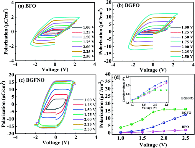 |
| | Fig. 2 (a) P–V loops of Au/BFO/NSTO (b) Au/BGFO/NSTO (c) Au/BGFNO/NSTO devices. (d) Dependence of remanent polarization and coercive field [inset of (d)] on the applied voltage. | |
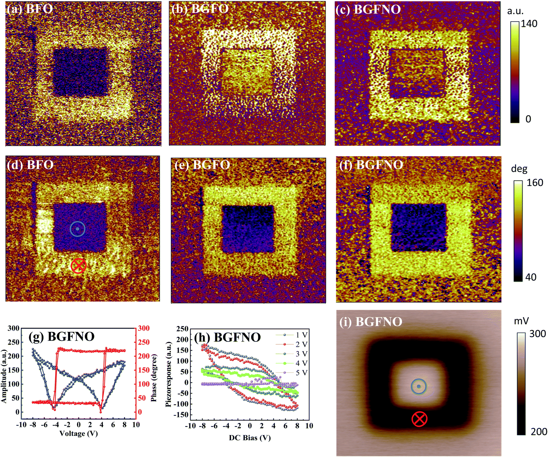
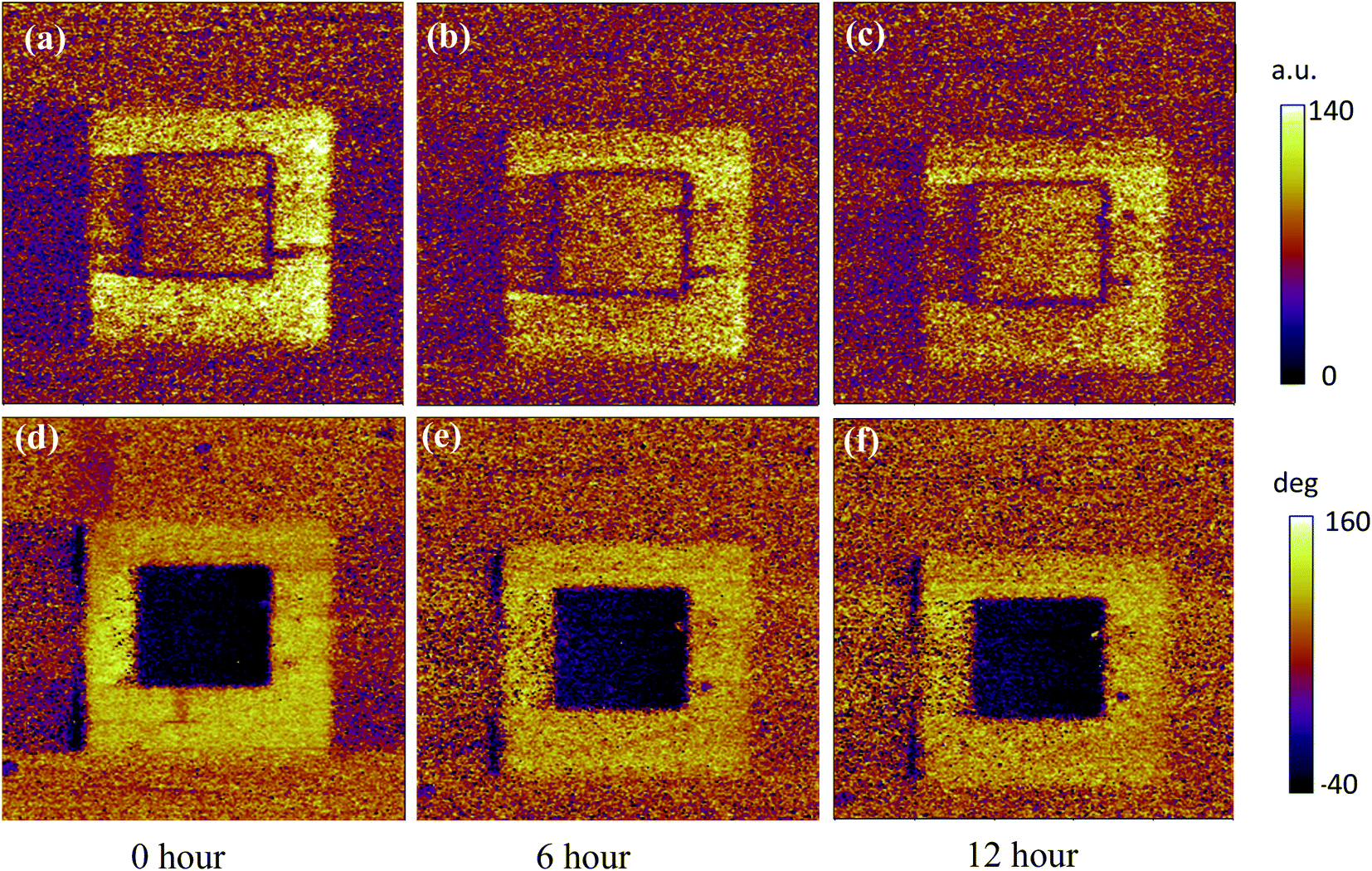
The local piezoresponse measurement is performed by PFM to explore the ferroelectric properties of the BFO, BGFO and BGFNO films. The PFM out-of-plane amplitude and phase images acquired after applying −6 V and +6 V biases on the surface of the BGFNO film are shown in Fig. 3(a–f). There is a significant polarization reversal in the area where the voltage is applied in the three films, the phase contrast of BGFNO films is closer to 180° compared to BFO and BGFO films, in addition, the domain walls are the clearest, implying that the BGFNO films has the best ferroelectricity. The hysteresis behavior of the butterfly-like amplitude and phase signals in Fig. 3(g) provides further evidence for ferroelectricity, and the local coercive voltages are about −4 V and +4 V. Furthermore, Strelcov et al. proposed a method of Vac-dependent PFM can distinguish ferroelectric and nonferroelectric origin.21 For ferroelectric material, piezoresponse (PR) hysteresis loop is expected to deform and even collapse when Vac is above the coercive voltage because the polarization switching counteracted the PR.22 The result in Fig. 3(h) is consistent with the literature, which suggests ferroelectric properties of BGFNO films. The BGFNO films are characterized using a Kelvin probe force microscope (KPFM). When measured at thermal equilibrium, the bias is applied to the sample, and the contact potential difference is the potential difference of the sample. Therefore, when the tip voltage is positive (negative), the negative (positive) ions and polarized charges will be attracted to the surface positive, which makes the surface potential lower (higher). This prediction is consistent with our observation in Fig. 3(i), which is attributed to ferroelectric polarization.23,24 The data in Fig. 3 further confirms the ferroelectric properties of the BGFNO films. In addition, the stability of the BGFNO film is measured as shown in Fig. 4 (a–f), the phase contrast and domain wall of the area of observation was retained for more than 12 h, indicating that this film exhibited superior piezoelectric properties for the storage applications.
 |
| | Fig. 3 (a–c) Corresponding PFM out-of-plane amplitude, and (d–f) PFM out-of-plane phase images acquired after applying a written bias of ±6 V with an AFM tip over an area of 5 × 5 μm2. (g) Phase and amplitude hysteresis loops of BGFNO/NSTO heterostructure. (h) PR signals and (i) SKPM image on BGFNO surface. | |
 |
| | Fig. 4 The out-of-plane PFM results for BGFNO over time after applying ±6 V bias (a–c) amplitude, and (d–f) phase images. | |
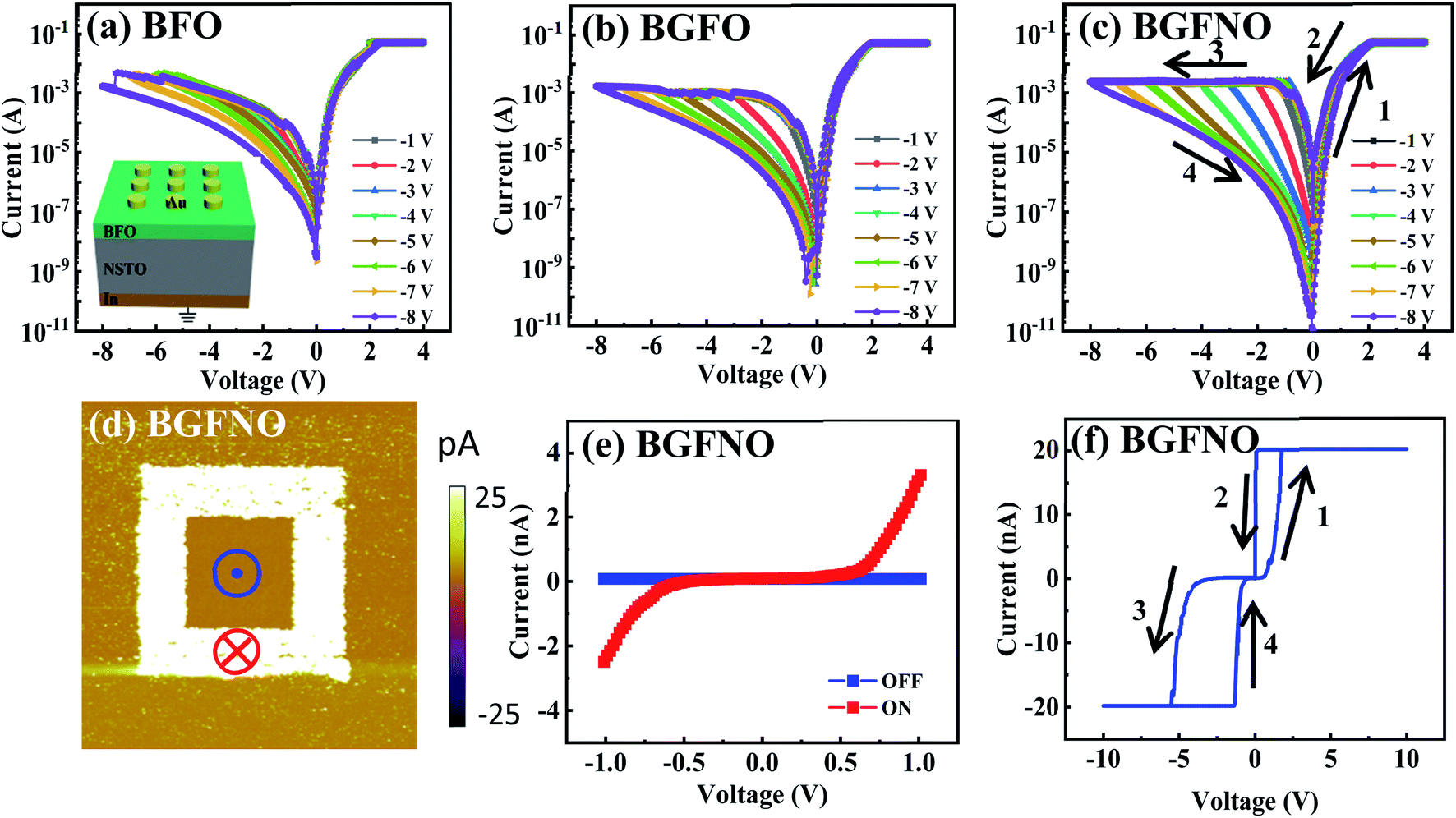
The current–voltage (I–V) characteristics of the Au/BFO/NSTO, Au/BGFO/NSTO and Au/BGFNO/NSTO heterojunction are conducted to study the multistage resistance conversion and polarization conversion behavior of the three thin films, as shown in Fig. 5(a–c). The positive direction of the current is defined from the top electrode to the bottom electrode, where the area of the top Au electrode is 4 × 10⁻⁴ cm2. The application sequence of voltage is 0 V → +4 V → 0 V →−Vmax → 0 V, and the arrows indicates the sweeping direction, as shown in Fig. 5(a–c). As can be seen from Fig. 5(a–c), leakage current decreases significantly with Gd and Ni co-doping. And the I–V curve of Au/BGFNO/NSTO devices have no significant RS window when the −Vmax is set to −1 V, but the RS window increases when the −Vmax increases. In addition, both the BFO and BGFO heterostructures exhibits multistage RS behaviors. All the I–V curves of the three devices show the obvious hysteretic behavior and asymmetric characteristics corresponding to the resistance switching behavior and rectification behavior, respectively. However, compared with BFO and BGFO films, the BGFNO films have a larger storage window at the same voltage as shown in Fig. 5(a–c). The typical CAFM measurements are performed in the same region of 5 × 5 μm2 to further study the local current switching characteristics of the BGFNO films. As shown in Fig. 5(d), there is a larger (smaller) current over the outer (central) domain after applying a ± 6 V of written bias over an area of 3 × 3 μm2. The conductivity of the downward polarized region is obviously higher than that of the upward polarized region. The current–voltage (I–V) curves are acquired from the areas with opposite polarization in Fig. 5(e), and the red (blue) line represents the state of downward polarization. These CAFM measurement results indicates a typical resistance switching effect in the BGFNO films.25 The local I–V curves of the BGFNO layers in Fig. 5(e and f) shows microscopic resistance switching properties. The I–V and CAFM results are well reproducible under the identical voltage sweeps.
 |
| | Fig. 5 I–V curves of (a) Au/BFO/NSTO (b) Au/BGFO/NSTO (c) Au/BGFNO/NSTO heterostructure on a semi-log scale. (d) Current map obtained by CAFM based on applying a written bias with a conductive tip. (e) Local I–V curves of two opposite polarization states (blue: up, and red: down) obtained using CAFM. (f) The local I–V curve. | |
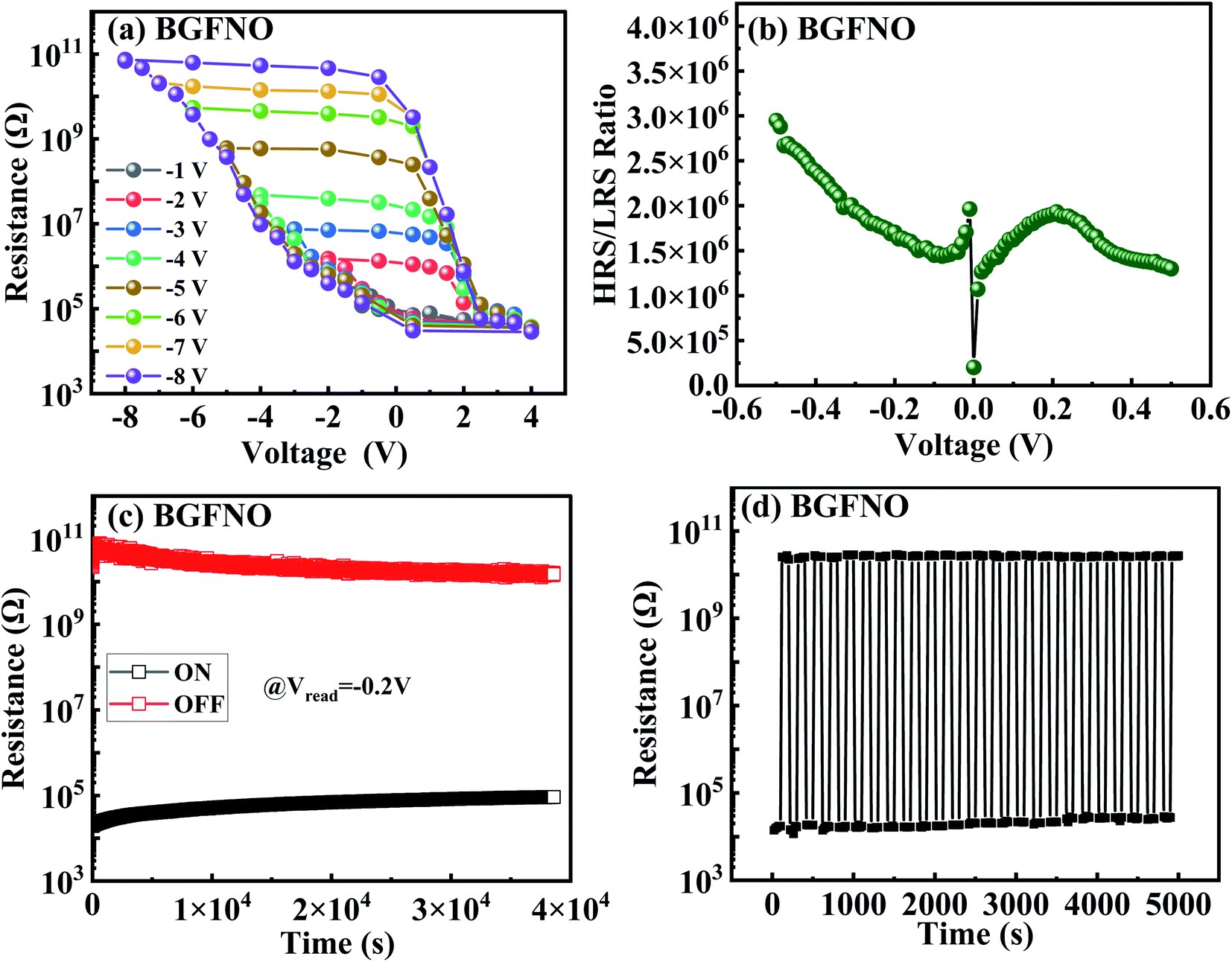
The non-volatile RS behavior is investigated using pulsed R–V measurements to further analyze the conventional bipolar RS and multistage RS behavior. In prior a voltage of +4 V is applied on the top electrode to set the device to the ON state,26 the resistance-voltage (R–V) loops are measured using a gradually increasing write voltage pulse with the maximum amplitude increasing from −1 V to −8 V and a constant read voltage of −0.2 V. A reset pulse of +4 V or −8 V is respectively applied to avoid the pre-history memory effect27 before the amplitude of negative pulses voltage changes from −1 V to −8 V. Fig. 6(a) shows the typical R–V hysteresis loop obtains at room temperature, which clearly illustrates the multi-level RS effect of the BGFNO/NSTO heterostructure as the value of −Vmax increases, and the RS window increases simultaneously. The resistance can be varied in several orders of magnitude by applying different write voltage pulses during the R–V measurements. The hysteresis change of the resistance with the write voltage is similar to that of the ferroelectric hysteresis loop, indicating that the ferroelectric polarization can modulate the resistance switching to some extent.26 The resistance increases with the increase of the negative voltage write pulse and decreases with the increase of the positive write voltage pulse, which is conducive to multi-state storage devices. Fig. 6(b) shows the on/off ratio as a function of reading voltage after applying a write voltage pulse of 100 ms with +4 V or −8 V, the maximum of on/off ratio reaches 3 × 10⁶. The device shows excellent retention of resistance after about 10 h in both the ON and OFF states in Fig. 6(c). And there is no obvious deterioration when the resistance switches back and forth between the two states repeatedly as shown in Fig. 6(d), which attests to the high stability of the sample.
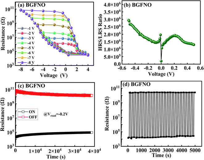 |
| | Fig. 6 (a) Typical R–V hysteresis loop and corresponding RS multilevel effect of the BGFNO heterostructure at room temperature. (b) HRS/LRS ratios of Au/BGFNO/NSTO samples. (c) Retention test of OFF and ON states. (d) Fatigue test of BGFNO heterostructure between OFF and ON states. | |
Discussion
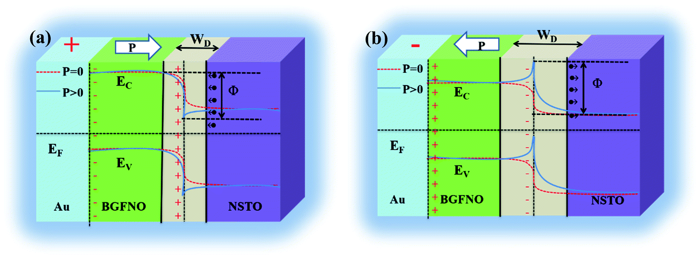
The BiFeO3 (BFO), Bi0.92Gd0.08FeO3 (BGFO) and Bi0.92Gd0.08Fe0.95Ni0.05O3 (BGFNO) films are prepared by the pulsed laser deposition system, the film quality and the remanent polarization are improved by gadolinium and nickel co-doping BiFeO3. And the Au/BGFNO/NSTO device exhibits larger storage window than that of Au/BGFO/NSTO and Au/BGFNO/NSTO devices due to the larger remanent polarization, so the CAFM and pulsed R–V tests are further performed, the results imply that resistance switching phenomenon can be attributed to the ferroelectric polarization reversal. The barrier height and width of the BGFNO/NSTO interface could be modified by applying an external electric field. As shown in Fig. 7(a), when a positive write voltage pulse is applied to the device, the BGFNO film is polarized downward, and the positive bound charges aggregated at the BGFNO/NSTO interface. The positive bound charges attract a lot of carriers in the NSTO substrate to the interface, the energy band bents down at the interface, and the device is set as the ON state. Hence, the width of the depletion regime decreases and corresponded to a low resistance state (LRS) in the resistive switching device. On the contrary, when the negative write voltage pulse is applied, the film is polarized upward. The device is set as the OFF state and a lot of carriers in the NSTO are repelled by the negative polarized bound charges at the interface, as shown in Fig. 7(b). The width of the depletion region increases and corresponded to a high resistance state (HRS) in the resistive switching device, which leads to the upward bending of the energy band at the interface. In addition, the depolarization field in the ferroelectric layer is generated in the opposite direction of the polarization and results in further band bending at the interface, which is due to the incomplete shielding of bound charges. Table 1 summarizes the HRS/LRS ratios for different structures.23,28–38 The large ratio is approximately 1000 times those of Pt/BFO/SRO and 10 times those of Pt/BLFO/NSTO, Pt/BSFO/NSTO and Pt/HZO/LSMO heterostructures in previous reports.23,29,31,34 Retention and fatigue tests show that the Au/BGFNO/NSTO heterostructure has high stability.
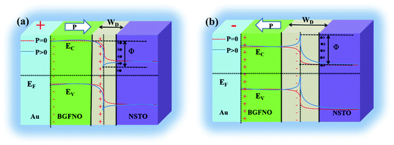 |
| | Fig. 7 (a) Schematic diagrams of the Au/BGFNO/NSTO heterostructure energy band at (a) LRS and (b) HRS. | |
Table 1 Experimental HRS/LRS ratio obtained with different ferroelectric heterojunctions
| Functional layer |
Top electrode |
Bottom electrode |
Year |
HRS/LRS ratio |
Ref. |
| BiFeO3 |
SrRuO3 |
Nb-doped SrTiO3 |
2015 |
593 |
28 |
| BiFeO3 |
Pt |
SrRuO3 |
2016 |
103 |
29 |
| BiFeO3 |
Co |
Ca0.96Ce0.04MnO3 |
2015 |
>104 |
30 |
| Sm-doped BiFeO3 |
Pt |
Nb-doped SrTiO3 |
2016 |
105 |
31 |
| La-doped BiFeO3 |
Pt |
Nb-doped SrTiO3 |
2020 |
2.8 × 10⁵ |
23 |
| Gd and Ni-doped BiFeO3 |
Au |
Nb-doped SrTiO3 |
|
3 × 10⁶ |
Our work |
| BaTiO3 |
MoS2 |
SrRuO3 |
2017 |
104 |
32 |
| BaTiO3 |
Pt |
Nb-doped SrTiO3 |
2013 |
>104 |
39 |
| BaTiO3 |
Pt |
Nb-doped SrTiO3 |
2019 |
105 |
33 |
| BaTiO3 |
Pt |
Nb-doped SrTiO3 |
2017 |
6 × 10⁶ |
34 |
| Zr-doped HfO2 |
TiN |
Pt |
2017 |
15 |
38 |
| Y-doped HfO2 |
Ag |
TiN |
2017 |
102 |
37 |
| Zr-doped HfO2 |
Pt |
Nb-doped SrTiO3 |
2021 |
8 × 10² |
35 |
| Zr-doped HfO2 |
Pt |
La0.7Sr0.3MnO3 |
2021 |
105 |
36 |
Conclusions
In summary, we prepared the BiFeO3 (BFO), Bi0.92Gd0.08FeO3 (BGFO) and Bi0.92Gd0.08Fe0.95Ni0.05O3 (BGFNO) films by the pulsed laser deposition system to form and demonstrated the ferroelectricity of these devices by PFM and P–V measurements. And the Au/BGFNO/NSTO heterojunction shows the large switching ratio of 3 × 10⁶ with stable bipolar resistance switching, good retention, and multi-level storage characteristics. The effective barrier height and width of the BGFNO/NSTO interface could be modified by applying an external electric field. This work provides an effective method to enhance remanent polarization and demonstrates the performance improvement of BiFeO3-based devices. BiFeO3-based heterostructures extends the functionality of BiFeO3-based heterostructures and has potential application in nonvolatile memories and logic devices.
Conflicts of interest
There are no conflicts to declare.
Acknowledgements
This work was supported by the National Natural Science Foundation of China (Grant No. 11974099), Intelligence Introduction Plan of Henan Province in 2021 (CXJD2021008), and Plan for Leading Talent of Fundamental Research of the Central China in 2020, Natural Science Foundation of Henan Province (202300410090), Key Scientific Research Project of Colleges and Universities in Henan Province (21A140005).
References
- M. M. Yang and M. Alexe, Adv. Mater., 2018, 30, 1704908 CrossRef PubMed.
- B. Sun, G. D. Zhou, L. Sun, H. Zhao, Y. Chen, F. Yang, Y. Zhao and Q. Song, Nanoscale Horiz., 2021, 6, 939–970 RSC.
- Y. Zhou, C. Wang, S. Tian, X. Yao, C. Ge, E.-J. Guo, M. He, G. Yang and K. Jin, Thin Solid Films, 2020, 698, 137851 CrossRef CAS.
- D. S. Knoche, M. Steimecke, Y. Yun, L. Muhlenbein and A. Bhatnagar, Nat. Commun., 2021, 12, 282 CrossRef CAS PubMed.
- F. Fan, M. Duan, B. Luo and C. Chen, Chin. J. Phys., 2018, 56, 1903–1908 CrossRef CAS.
- P. Jain, Q. Wang, M. Roldan, A. Glavic, V. Lauter, C. Urban, Z. Bi, T. Ahmed, J. Zhu, M. Varela, Q. X. Jia and M. R. Fitzsimmons, Sci. Rep., 2015, 5, 9089 CrossRef CAS PubMed.
- W. Jin Hu, Z. Wang, W. Yu and T. Wu, Nat. Commun., 2016, 7, 10808 CrossRef PubMed.
- L. T. Mai Oanh, D. V. Thang, D. D. Bich, P. D. Chung, N. M. Hung, N. Van Quang and N. Van Minh, Ceram. Int., 2020, 46, 17423–17429 CrossRef.
- T. K. Lin, H. W. Chang, Y. H. Sung, C. R. Wang, D. H. Wei, C. S. Tu and W. C. Chang, Mater. Lett., 2020, 276, 128216 CrossRef CAS.
- J. G. Wu, D. Q. Xiao and J. G. Zhu, Chin. Sci. Bull., 2014, 59, 5205–5211 CrossRef CAS.
- X. L. Deng, Z. X. Zeng, R. L. Gao, Z. h. Wang, G. Chen, W. Cai and C. Fu, J. Alloys Compd., 2020, 831, 154857 CrossRef CAS.
- S. J. Yang, F. Q. Zhang, X. B. Xie, X. Guo, L. Zhang and S. Fan, J. Mater. Sci.: Mater. Electron., 2017, 28, 14944–14948 CrossRef CAS.
- P. M. Razad, K. Saravanakumar, V. Ganesan, V. R. Reddy, R. J. Choudhary, K. Jeyadheepan and K. Mahalakshmi, J. Mater. Sci.: Mater. Electron., 2019, 30, 18306–18314 CrossRef CAS.
- S. S. Rajput, R. Katoch, K. K. Sahoo, G. N. Sharma, S. K. Singh, R. Gupta and A. Garg, J. Alloys Compd., 2015, 621, 339–344 CrossRef CAS.
- Y. Zheng, G. Tan, A. Xia and H. Ren, Mater. Lett., 2016, 173, 18–21 CrossRef CAS.
- P. P. Biswas, S. Pal, V. Subramanian and P. Murugavel, Appl. Phys. Lett., 2019, 114, 173901–173905 CrossRef.
- F. Liu, F. Q. Ji, Y. L. Lin, S. F. Huang, X. J. Lin and F. Yang, ACS Appl. Nano Mater., 2020, 3, 8888–8896 CrossRef CAS.
- G. D. Hu, X. Cheng, W. B. Wu and C. H. Yang, Appl. Phys. Lett., 2007, 91, 232909 CrossRef.
- Y. Liu, J. Wei, Y. Guo, T. Yang and Z. Xu, RSC Adv., 2016, 6, 96563–96572 RSC.
- T. T. Yang, J. Wei, Z. B. Lv, Y. Guo and Z. Xu, J. Sol-Gel Sci. Technol., 2018, 88, 618–627 CrossRef CAS.
- E. Strelcov, Y. Kim, J. C. Yang, Y. H. Chu, P. Yu, X. Lu, S. Jesse and S. V. Kalinin, Appl. Phys. Lett., 2012, 101, 192902 CrossRef.
- Q. X. Li, C. H. Jia, Y. Zhang and W. F. Zhang, ACS Appl. Electron. Mater., 2021, 3, 1787–1793 CrossRef CAS.
- W. Q. Dai, Y. X. Li, C. H. Jia, C. Y. Kang, M. X. Li and W. F. Zhang, RSC Adv., 2020, 10, 18039–18043 RSC.
- Z. Fan, H. Fan, L. Yang, P. L. Li, Z. X. Lu, G. Tian, Z. F. Huang, Z. W. Li, J. X. Yao, Q. Y. Luo, C. Chen, D. Y. Chen, Z. B. Yan, M. Zeng, X. B. Lu, X. S. Gao and J. M. Liu, J. Mater. Chem. C, 2017, 5, 7317–7327 RSC.
- C. Jia, J. Li, G. Yang, Y. Chen and W. Zhang, Nanoscale Res. Lett., 2018, 13, 102 CrossRef PubMed.
- X. Chen, C. H. Jia, Y. H. Chen, G. Yang and W. F. Zhang, J. Phys. D: Appl. Phys., 2014, 47, 365102 CrossRef.
- D. J. Kim, H. Lu, S. Ryu, C. W. Bark, C. B. Eom, E. Y. Tsymbal and A. Gruverman, Nano Lett., 2012, 12, 5697–5702 CrossRef CAS PubMed.
- L. Zhao, Z. Lu, F. Zhang, G. Tian, X. Song, Z. Li, K. Huang, Z. Zhang, M. Qin, S. Wu, X. Lu, M. Zeng, X. Gao, J. Dai and J. M. Liu, Sci. Rep., 2015, 5, 9680 CrossRef CAS PubMed.
- Z. Lu, Z. Fan, P. Li, H. Fan, G. Tian, X. Song, Z. Li, L. Zhao, K. Huang, F. Zhang, Z. Zhang, M. Zeng, X. Gao, J. Feng, J. Wan and J. Liu, ACS Appl. Mater. Interfaces, 2016, 8, 23963–23968 CrossRef CAS PubMed.
- S. Boyn, V. Garcia, S. Fusil, C. Carrétéro, K. Garcia, S. Xavier, S. Collin, C. Deranlot, M. Bibes and A. Barthélémy, APL Mater., 2015, 3, 061101 CrossRef.
- L. Wang, M. R. Cho, Y. J. Shin, J. R. Kim, S. Das, J. G. Yoon, J. S. Chung and T. W. Noh, Nano Lett., 2016, 16, 3911–3918 CrossRef CAS PubMed.
- T. Li, P. Sharma, A. Lipatov, H. Lee, J.-W. Lee, M. Y. Zhuravlev, T. R. Paudel, Y. A. Genenko, C.-B. Eom, E. Y. Tsymbal, A. Sinitskii and A. Gruverman, Nano Lett., 2017, 17, 922–927 CrossRef CAS PubMed.
- J. Li, N. Li, C. Ge, H. Huang, Y. Sun, P. Gao, M. He, C. Wang, G. Yang and K. Jin, iScience, 2019, 16, 368–377 CrossRef CAS PubMed.
- Z. Xi, J. Ruan, C. Li, C. Zheng, Z. Wen, J. Dai, A. Li and D. Wu, Nat. Commun., 2017, 8, 15217 CrossRef CAS PubMed.
- P. Jiao, Z. Xi, X. Zhang, Y. Han, Y. Wu and D. Wu, Appl. Phys. Lett., 2021, 118, 252901 CrossRef CAS.
- B. Prasad, V. Thakare, A. Kalitsov, Z. Zhang, B. Terris and R. Ramesh, Adv. Electron. Mater., 2021, 7, 2001074 CrossRef CAS.
- X. Tian and A. Toriumi, IEEE Electron Devices Technology and Manufacturing Conference, (Edtm), 2017, pp. 63–64 Search PubMed.
- F. Ambriz-Vargas, G. Kolhatkar, M. Broyer, A. Hadj-Youssef, R. Nouar, A. Sarkissian, R. Thomas, C. Gomez-Yanez, M. A. Gauthier and A. Ruediger, ACS Appl. Mater. Interfaces, 2017, 9, 13262–13268 CrossRef CAS PubMed.
- Z. Wen, C. Li, D. Wu, A. D. Li and N. B. Ming, Nat. Mater., 2013, 12, 617–621 CrossRef CAS PubMed.
|
| This journal is © The Royal Society of Chemistry 2022 |
Click here to see how this site uses Cookies. View our privacy policy here. 
 Open Access Article
 This Open Access Article is licensed under a Creative Commons Attribution-Non Commercial 3.0 Unported Licence
 a,
Qiyuan Wua,
Caihong Jiaa,
Zhaomeng Gaob and
Weifeng Zhang*a
a,
Qiyuan Wua,
Caihong Jiaa,
Zhaomeng Gaob and
Weifeng Zhang*a