
 Open Access Article
 This Open Access Article is licensed under a
 Creative Commons Attribution 3.0 Unported Licence
Pattern formation in thin polymeric films via electrohydrodynamic patterning
Guowei Lv
 ab,
Hongmiao Tian
c,
Jinyou Shao
c and
Demei Yu
*a
ab,
Hongmiao Tian
c,
Jinyou Shao
c and
Demei Yu
*a
aSchool of Chemistry, State Key Laboratory of Electrical Insulation and Power Equipments, MOE Key Laboratory for Non-Equilibrium Synthesis and Modulation of Condensed Matter, Xi'an Jiaotong University, Xi'an 710049, Shaanxi, P. R. China. E-mail: dmyu@xjtu.edu.cn
bXi'an Aerospace Chemical Propulsion Co., Ltd., Xi'an 710025, Shaanxi, P. R. China
cState Key Laboratory of Manufacturing Systems Engineering, Xi'an Jiaotong University, Xi'an 710049, Shaanxi, P. R. China
First published on 28th March 2022
Abstract
The free surface of a thin polymeric film is often unstable and deforms into various micro-/nano-patterns under an externally applied electric field. This paper reviews a recent patterning technique, electrohydrodynamic patterning (EHDP), a straightforward, cost-effective and contactless bottom-up method. The theoretical and numerical studies of EHDP are shown. How the characteristic wavelength and the characteristic time depend on both the external conditions (such as voltage, film thickness, template-substrate spacing) and the initial polymer properties (such as rheological property, electrical property and surface tension) is theoretically and experimentally discussed. Various possible strategies for fabricating high-aspect-ratio or hierarchical patterns are theoretically and experimentally reviewed. Aligning and ordering of the anisotropic polymers by EHDP is emphasized. A perspective, including novelty and limitations of the methods, particularly in comparison to some conventional patterning techniques, and a possible future direction of research, is presented.
 Guowei Lv | Guowei Lv received his PhD degree in materials science and engineering from Xi'an Jiaotong University, Xi'an, China, in 2017. He is currently an Assistant Research Fellow of Xi'an Aerospace Chemical Propulsion Co., Ltd. He has authored/coauthored more than 20 research papers in international journal and conference proceedings. His research interests include conducting polymer and patterning. |
 Hongmiao Tian | Hongmiao Tian received his PhD degree in mechanical engineering from Xi'an Jiaotong University, Xi'an, China, in 2014. He is currently an Associate Professor with the State Key Laboratory for Manufacturing Systems Engineering, Xi'an Jiaotong University. He has authored/coauthored more than 70 research papers in international journal and conference proceedings and authorized 30 national invention patents. His research interests include bionic manufacturing and soft actuators. |
 Jinyou Shao | Jinyou Shao received his PhD degree in mechanical engineering from Xi'an Jiaotong University, Xi'an, China, in 2009. He is currently the President of Frontier Institute of Science and Technology (FIST), a Professor at the State Key Laboratory for Manufacturing Systems Engineering, Xi'an Jiaotong University, and the leader of the Youth Innovation Team of Shaanxi Universities. His research interests include micro/nano-manufacturing techniques, flexible electronics, nanosensors and devices, etc. Dr Shao is awarded NSFC Fund for Distinguished Scholars, NSFC Fund for Excellent Young Scholars, Changjiang Scholars –Young Category, New Century Excellent Talents by MoE of China, Shaanxi Young Talents in Science and Technology, etc. |
 Demei Yu | Demei Yu received her PhD degree from Xi'an Jiaotong University, Xi'an, China, in 1998. She joined Xi'an Jiaotong University in 1984, and served as professor and founding chair of the Department of Applied Chemistry in Xi'an Jiaotong University since 2001. In addition, she is also a professor and lab committee member of State Key Lab of Electrical Insulation and Power Equipment in Xi'an Jiaotong University since 2004. Her research interests include: (1) design and fabrication of functional micro-/nano-materials; (2) synthesis and preparation of smart polymer (conductive polymers, electroactive polymers); (3) design and preparation of polymer micro-/nano-composites with high performance (electrical, thermal and mechanical properties); (4) polymer processing and polymer rheology. |
1 Origin of EHDP
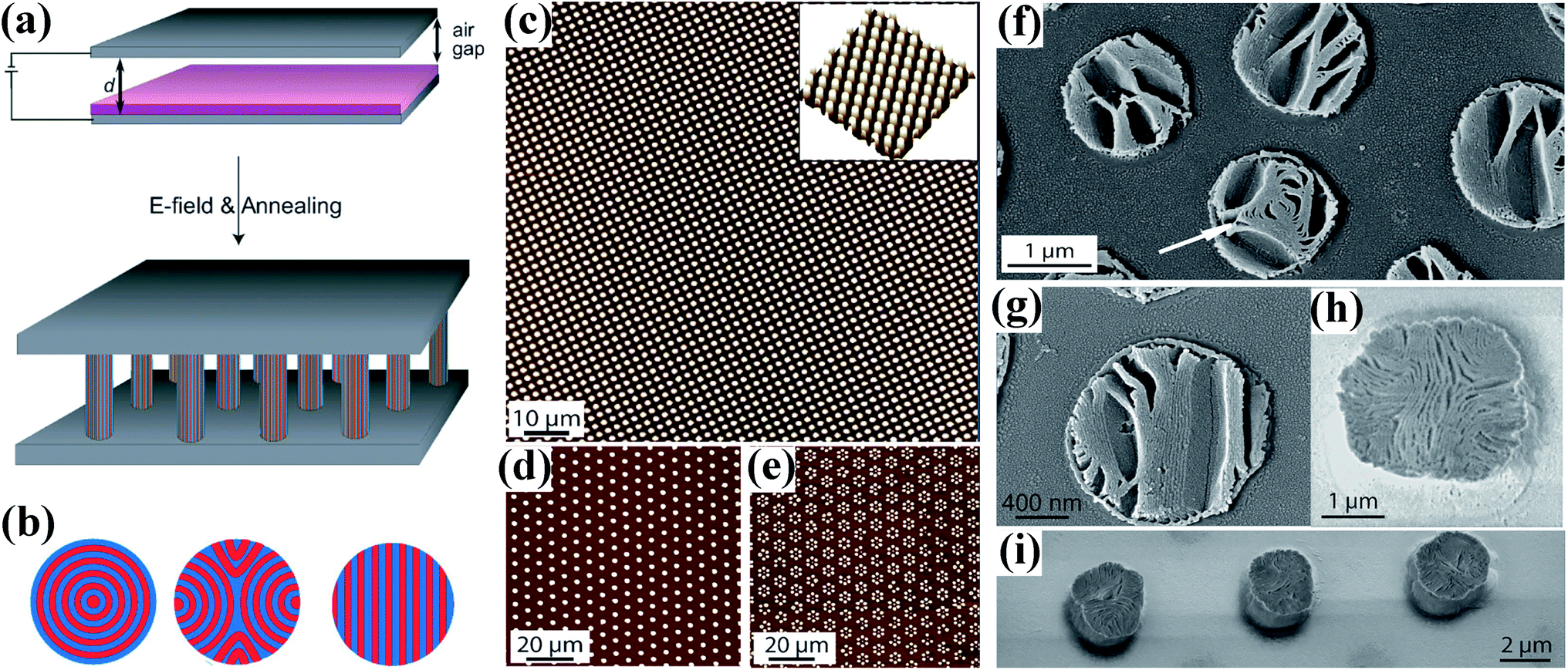
Over the past few decades, the urgent need of micro- and nano-structures for manufacturing high-performance devices, such as integrated circuits, optoelectronic devices, and sensor arrays, has motivated the development of new patterning techniques.1–5 In 1999, Chou et al. observed that a periodic pillar array with a micrometer scale was formed in a thin polymer film.6–14 Although without the external electric field, the key driving force for the formation of the micro-/nano-structures is the internal localized electrical field generated between the contactor and the polymer film. In 2000, Schaffer et al. reported a straightforward, cost-effective and contactless (positive replica) patterning technique, electrohydrodynamic patterning (EHDP), that creates and replicates lateral hierarchical structures with a submicrometre length scale on various kinds of materials (e.g. thermoplastic polymer,15–22 thermosetting polymer,23–29 photocurable resin,30–34 ceramic,35–37 and so on) under an externally applied electric field.38–47 Especially, the capability of EHDP with a featureless template to fast and economically create large-scale three-dimensional micro-scale structures, even though no long range order, is particularly attractive because the difficulty, time, and cost in designing and making pre-patterned templates limit the flexibility and wide application of conventional lithography, especially when large numbers of different patterns are to be fabricated.48 It is worth noting that a higher value of f (h/H, the ratio of the polymer film thickness to the template-substrate spacing) leads to a denser packing of the polymer columns and to an enhanced electrostatic repulsion between the equally charged columns, resulting in columns with a perfect hexagonal symmetry and, however, an accelerating coarsening.,15 a lower value of f leads to the suppression of coarsening.49,50 Hence, the highly ordered arrays of columns only can be obtained in a very narrow f range.51 In addition, EHDP just need a minimized external force to maintain a proper air gap between the liquid polymer and the template, avoiding a poor geometrical integrity of the duplicated micro-/nano-structure or even to an irreversible damage of the substrate and the template.52The diagrammatic sketch of EHDP is shown in Fig. 1.53 Firstly, a thin film of the polymer is spin-coated on a conductive substrate (bottom electrode). Then a template (top electrode) is put on the top of the polymer film, leaving an air gap. Secondly, the assembly is then thermally maintained above the glass transition temperature (Tg) of the polymer, and then an external voltage is applied between the bottom and top electrode. This applied voltage causes a destabilizing electrostatic force due to the mismatch of the dielectric constant or the electrical conductivity between polymer and air. Once the destabilizing electrostatic force overcomes the stabilizing surface tension and the viscous resistance, the flat polymer surface will be destabilized and forced to flow upward to the top electrode. The growth of peaks reduces the air gap between the polymer film and the template, which strengthens the electrical field and accelerates the evolution. As the peaks grow, the capillary pressure also increases. Therefore, the competition between destabilizing electrostatic pressure and the stabilizing capillary pressure selects a maximum characteristic wavelength λ and a characteristic time τ.48 Finally, the micro-/nano-structure of the polymer will fully contact with the top electrode and then reach a steady state. After that, a slow cooling of the assembly to room temperature or UV light cures the micropillars array. In this process, the template can be either featureless (Fig. 1a),15,17,27 generating an array of periodic pillars, or patterned (Fig. 1b),15,37,39,41,46,54–65 forming a positive replica of the template.
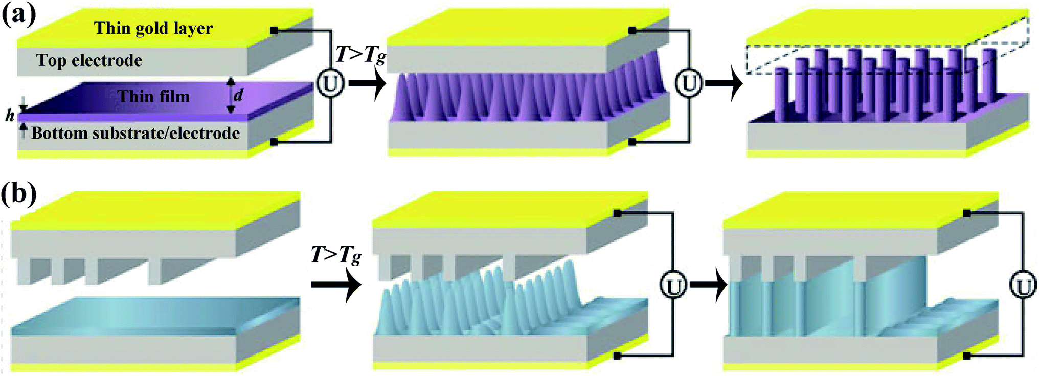 | ||
| Fig. 1 The diagrammatic sketch of EHDP with (a) a featureless template and (b) a patterned template. Reproduced with permission.66 Copyright 2013, Springer International Publishing Switzerland. | ||
2 Theoretical and numerical studies
The overall pressure distribution at the viscous film surface is| p(h) = p0 + pvdW(h) + pγ(h) + pe(h) | (1) |
For high enough values of electric field intensity, only the Laplace and electrostatic terms need to be considered. In a stability analysis, a small sinusoidal perturbation of the interface with wave number q, growth rate ω, and amplitude u is considered: h(x, t) = h0 + ueiqx+tω. The modulation of h gives rise to a lateral pressure gradient inside the film, inducing a Poiseuille flow j
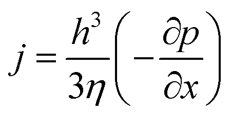 | (2) |
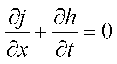 | (3) |
Eqn (1)–(3) establish a differential equation that describes the dynamic response of the interface to the perturbation. In a linear approximation, a dispersion relation is obtained
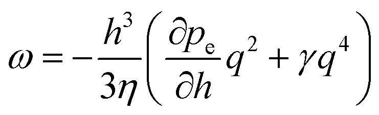 | (4) |
As opposed to the inviscid, gravity-limited case (ω ∝ q), the viscous stresses lead to a q2-dependence of ω in the long-wavelength limit, typical for dissipative systems. Fluctuations are amplified if ω > 0. With time, the fastest growing fluctuation will eventually dominate
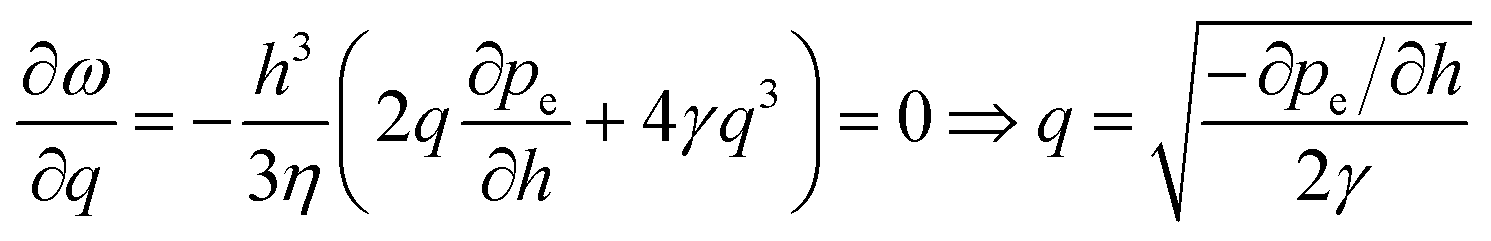 | (5) |
When mobile free charge is absent (i.e. perfect dielectric), the characteristic wavelength λ and the characteristic time τ is
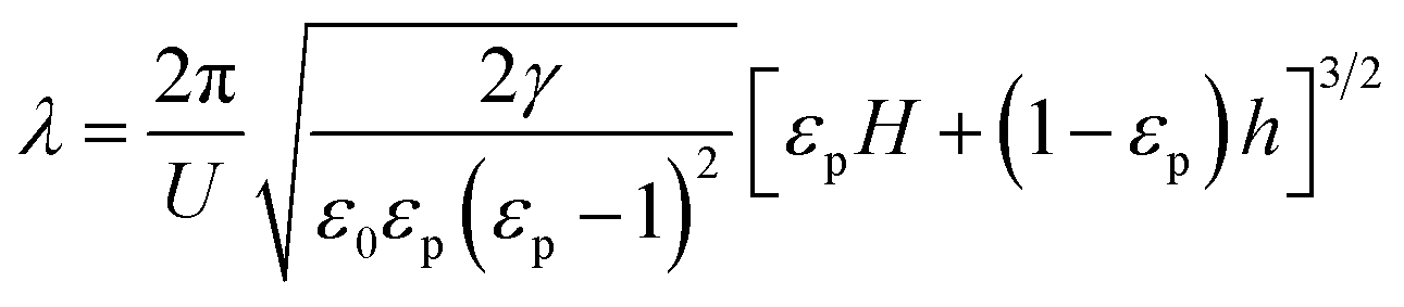 | (6) |
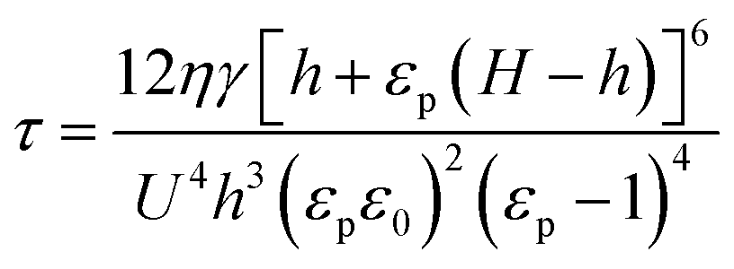 | (7) |
When mobile free charge is present (i.e. leaky dielectric), the dielectric constant and a dimensionless conductivity parameter S jointly play roles. The latter represents a ratio of the process time scale to the time for charge conduction (εgε0/σ)
| S = σηγH3/ε03U4 | (8) |
Especially, when S ≫ 1, the characteristic wavelength λ and the characteristic time τ is
 | (9) |
 | (10) |
3 Effect of the external conditions on the pattern formation
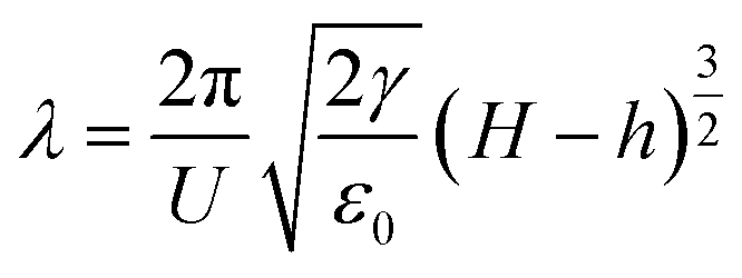
In continuing the steady development of integrated circuit-related fabrication, the ability to rapidly pattern polymers into smaller feature size and/or higher aspect ratio in order to realize devices with enhanced performance or even wholly new properties begins to take a more prominent role in their advanced applications.According to eqn (6)–(10), changing the external conditions such as decreasing the template-substrate spacing (H), increasing the polymer film thickness (h) and increasing the applied voltage (U) can fabricate micro-/nano-patterns with a shorter characteristic time and a smaller characteristic wavelength via EHDP for both the perfect and leaky dielectric. For example, Russel et al. showed that the characteristic wavelength λ decreases with the increase in the applied voltage (below 10 V) at a given system, as shown in Fig. 2a.71 However, the characteristic wavelength λ no longer decreases or even increases with the increase in the applied voltage (above 10 V) due to the dielectric breakdown in at least one of the layers. If layers break down, submicrometer features are unlikely, as shown in Fig. 2b. Hence, though theory predicts that changing the external conditions will decrease the characteristic wavelength λ to nanoscale level, the limit is set by the dielectric field strength of the layers. In addition, increasing the pattern growth velocity not only shortens the patterning time but also exhibits enhanced scalability for replicating small and geometrically diverse features.72
 | ||
| Fig. 2 EHDP of PMMA2K-air. (a) Plot of the characteristic wavelength λ vs. the applied voltage. (b) An optical micrograph of pillars formed at 10 V. Reproduced with permission.71 Copyright 2011, American Chemical Society. | ||
4 Effect of the polymer properties on the pattern formation
In EHDP, polymer film materials have played a critical role, since some limitations in accessing better-performance EHDP, such as higher efficiency, smaller feature size, and greater aspect ratio, are of material origin; moreover, the functionality of the generated EHD patterns is governed by EHD materials owing to the interesting properties these materials can offer. Hence, the performance of EHDP depends on the comprehensive properties of the polymer film to a certain extent.4.1 Rheological property
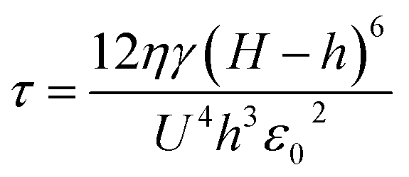
The rheological property of the polymer noticeably governs the characteristic wavelength λ and the characteristic time τ of EHDP.23–27,73–75 Sharma et al. has systematically studied the role of the viscoelastic property of the polymer film in the pattern formation of EHDP.24 The viscoelastic films behaving like a liquid display long wavelengths governed by applied voltage (or electrostatic pressure) and surface tension, independent of its elastic storage and viscous loss moduli (Fig. 3a(i)); the viscoelastic films behaving like a solid display wavelengths always scales as ∼4 × film thickness, independent of its surface tension, applied voltage, loss and storage moduli (Fig. 3a(ii)); and the viscoelastic films behaving in a narrow transition zone between the liquidlike and the solidlike regimes display a wavelength governed by the storage modulus (Fig. 3a(iii)). It is interesting to note that the viscosity of the polymer film influences the characteristic time τ of EHDP. This offers an advantage in EHDP for decoupling time by varying the types or the molecular weight of polymers. For example, Dickey et al. showed that the photocurable systems (e.g. thiol vinyl ether, vinyl ether, thiol acrylate, DMS acrylate, epoxy) with a low viscosity (0.1–1.8 Pa s) formed pillar arrays nearly instantaneously under ambient conditions.30,76 Goldberg-Oppenheimer et al. showed that the use of the polymers with a low-viscosity (0.073–1.032 Pa s) evidently reduced the characteristic time.19 It is worth noting that the rheology property of the polymer is closely related to its temperature. For instance, Cheng et al. showed a faster growth of the surface patterns of polystyrene film at a higher temperature due to the lower viscosity.20 However, the molding temperature cannot exceed the decomposition temperature of the polymer in the pattern formation process. | ||
| Fig. 3 (a(i)) The characteristic wavelength λ vs. VE−3 in log–log scale for viscoelastic liquidlike films. (ii) The characteristic wavelength λ vs. the film thickness h for viscoelastic solidlike films. (iii) The characteristic wavelength λ vs. the storage modulus μ for viscoelastic films between the liquidlike and the solidlike regimes. Reproduced with permission.24 Copyright 2009, American Physical Society. (b) Optical microscopy image of EHDP patterns of (i) a thin liquid film of PI and (ii) a bilayer of PI and ODMS. Reproduced with permission.77 Copyright 2001, American Institute of Physics. (c) EHDP patterns of various Au(PS) thin films: (i) Au(PS) 0 vol%; (ii) Au(PS) 0.05 vol%; (iii) Au(PS) 0.25 vol%; (iv) Au(PS) 0.5 vol%; (v) Au(PS) 1.0 vol%. Reproduced with permission.78 Copyright 2008, American Chemical Society. (d and e) Simulated and experimental deformation of EHDP with (d) a featureless template and (e) a structured template for (i) the leaky dielectric and (ii) perfect dielectric. Reproduced with permission.33 Copyright 2016, Royal Society of Chemistry. Reproduced with permission.31 Copyright 2014, American Chemical Society. | ||
4.2 Surface/interface tension
The decrease of the surface/interface tension of the polymer film is advantageous to fabricating the micro-/nanostructures with a smaller characteristic wavelength λ and a shorter characteristic time τ.75,77,79–85 For example, a clear reduction in length scale (2 times) and time scale (50 times) of polyisoprene (PI) film is observed by substituting the air gap with oligomeric dimethylsiloxane (ODMS) film, as shown in Fig. 3b. However, there is a trade-off by replacing air with another fluid because it may decrease the dielectric contrast difference of the system.484.3 Electrical property
Especially, the conducting polymer (CP), as a leaky dielectric, is a promising material for high-performance EHDP in order to realize devices with enhanced performance or even wholly new properties and then take a more prominent role in their advanced applications such as organic electronic devices, chemical sensors, field-effect transistors, superhydrophilic/superhydrophobic surfaces, micro-/nanofluidic systems and micro-/nanoelectromechanical systems (MEMS/NEMS).93–99 For instance, Rickard et al. fabricated well-defined conductive micro-/nano-structures using the thin conducting polymer (e.g. polypyrrole, poly(3-hexylthiophene), and so on) films via EHDP, as shown in Fig. 4a–f.100–102 Moreover, they showed the feasibility of the polypyrrole-based structures with a gate length of 700 nm and a pitch of 500 nm for the electrolyte-gated vertical field-effect transistor (FET) devices, as shown in Fig. 4g–h.
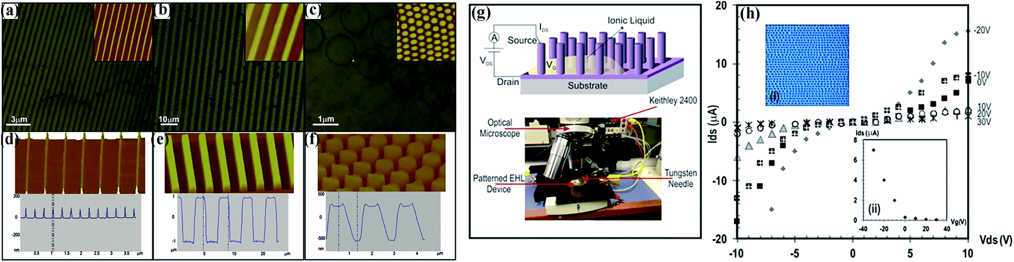 | ||
| Fig. 4 (a–f) Optical microscopy images with height AFM images (inset) and three-dimensional AFM micrographs with cross section analysis of EHDP patterns of PPy. (g) Schematic representation (top) and an overview image (bottom) of the configuration of a liquid-ion gate vertical FET using the EHDP patterns on the top of a Si–SiO2 substrate. (h) Drain current versus drain voltage characteristics of PPY electrolyte-gated transistor based on (i) EHDP pillars shown in a top-view optical image and (ii) gate voltage performance of the PPy-FET. Reproduced with permission from https://pubs.acs.org/doi/10.1021/acsnano.6b01246.100 Copyright 2016, American Chemical Society (notice: further permissions related to the material excerpted should be directed to the ACS). | ||
5 Fabrication of hierarchical structures
To date, several techniques structure a single layer of the polymer. For many applications, however, it is desirable to control the spatial arrangement of more than one component. Morariu et al. describes a replication process where multiple materials with an air gap between the film and the contactor are processed simultaneously, as shown in Fig. 5a.103–112 Using a bilayer or trilayer formed by two or three different polymers, EHDP at both polymer surfaces produce a hierarchic lateral structure that exhibits two or three independent characteristic dimensions, as shown in Fig. 5b–e.103–112 This approach might provide a simple strategy for large-area, sub-100 nanometre lithography.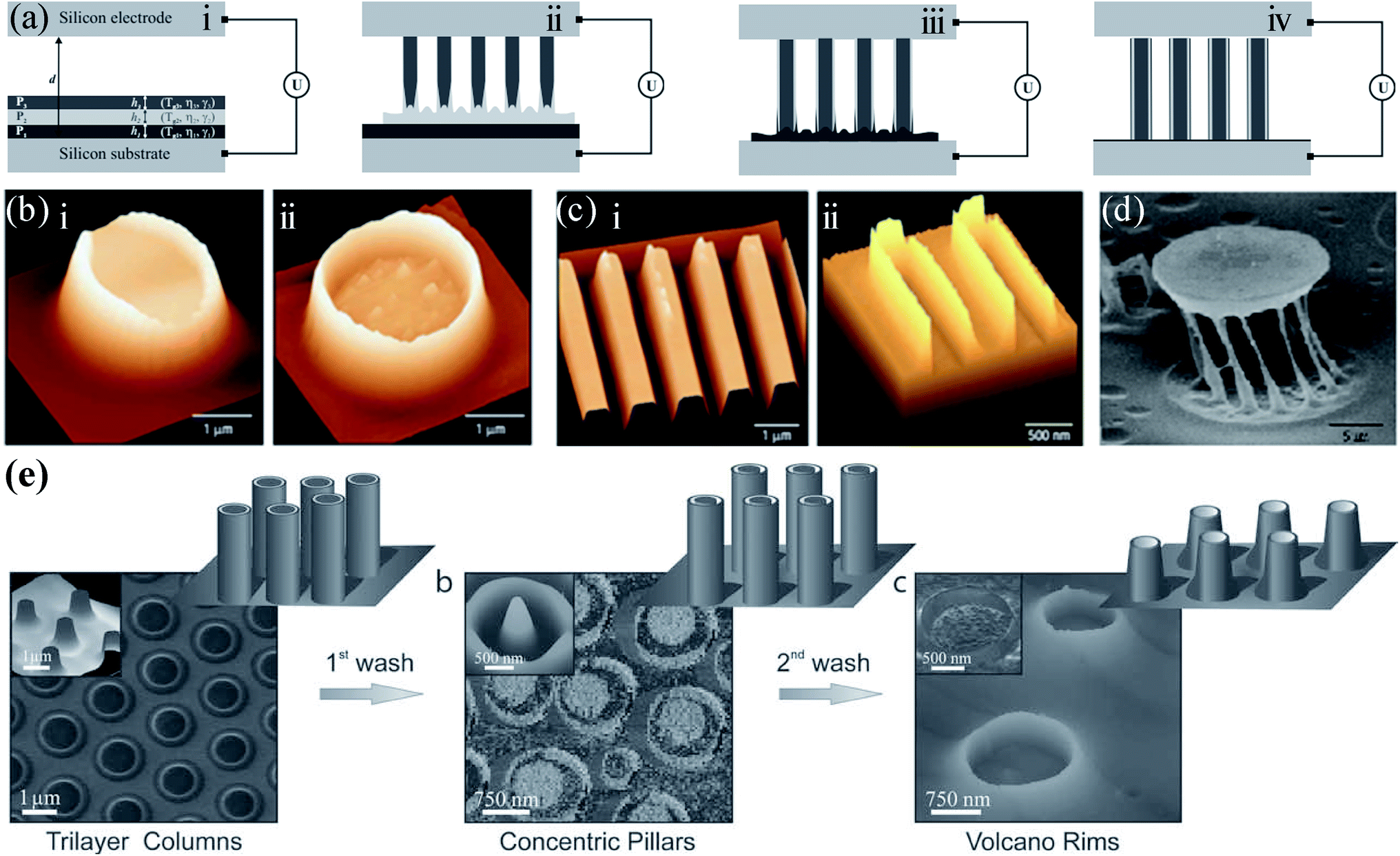 | ||
| Fig. 5 (a) Mechanism of the EHDP structure formation process for multilayer system. Reproduced with permission.106 Copyright 2012, WILEY-VCH. (b and c) EHDP with (b) a featureless template and (c) a patterned template patterns of a PMMA-PS-air bilayer: AFM image of a single column before (i) or after (ii) removing the PS core by washing in cyclohexane. Reproduced with permission.103 Copyright 2002, Nature Publishing Group. (d) EHDP patterns of a PS-PMMA-air bilayer: SEM image of a single “cage” after removing the PS core by washing in cyclohexane. Reproduced with permission.105 Copyright 2006, American Chemical Society. (e) EHDP patterns of an EC-PVA-PVAc-air trilayer: AFM and SEM images of structures derived from (i) the trilayer coaxial pillars, (ii) central PVAc pillars surrounded by thin EC rims, and (iii) EC nanovolcanos. Reproduced with permission.106 Copyright 2012, WILEY-VCH. | ||
EHDP with a featureless template shows the capability to fast and economically create large-scale three-dimensional micro-scale structures on various kinds of materials. However, conventional EHDP with a featureless template can only fabricate a low-aspect-ratio micro-/nanostructures. Therefore, much research have been devoted to increase the aspect ratio of the micro-/nanostructures.113,114 For instance, Tian et al. developed a novel EHDP technique, EHDP-prepatterned polymer (PPP), to fabricate a hierarchical micro-/nanostructure with a high aspect ratio, as shown in Fig. 6a.114 The simulation and experiment showed that EHDP-PPP approach can provide a stronger electric modulation at the same experimental settings, obtaining a hierarchical micro-/nanostructure with a higher aspect ratio compared to EHDP-prepatterned template (PPT), as shown in Fig. 6b. This method can deform various polymers to a mushroom-shaped micropillars with a well-controlled aspect ratio and tip diameter for dry adhesion, nanogenerator, superhydrophilic/superhydrophobic surfaces, microlens arrays, and so on, as shown in Fig. 6c.115–123 Furthermore, to fabricate a hierarchically ordered structure, Tian et al. improved above EHDP-PPP method by substituting the featureless template with a patterned template which feature size is far less than the characteristic wavelength λ of the given system, as shown in Fig. 7a and b. The hierarchically ordered structures with primary and secondary patterns for mass-production, such as, micropillar/nanopillar structure, micrograting/micropillar structure, micropillar/micrograting structure, and micrograting/micrograting structure, were fabricated, as shown in Fig. 7c.124,125
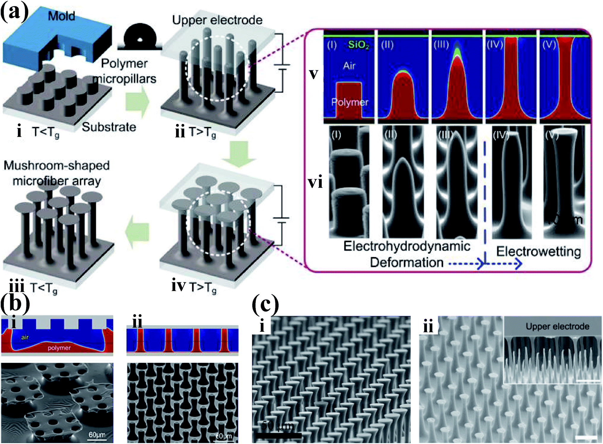 | ||
| Fig. 6 (a) Illustration of a three-step process for fabricating a bioinspired mushroom-shaped microfiber array with a high aspect ratio. Reproduced with permission.115 Copyright 2014, American Chemical Society. (b) Simulated and experimental structures fabricated by (i) EHDP-PPT and by (ii) EHDP-PPP. Reproduced with permission.114 Copyright 2014, American Chemical Society. (c) The mushroom-shaped micropillars with a well-controlled aspect ratio and tip diameter using various polymers: (i) polymethyl methacrylate (PMMA) and (ii) polyvinylidene fluoride (PVDF). Reproduced with permission.115 Copyright 2014, American Chemical Society. Reproduced with permission.116 Copyright 2015, Royal Society of Chemistry. | ||
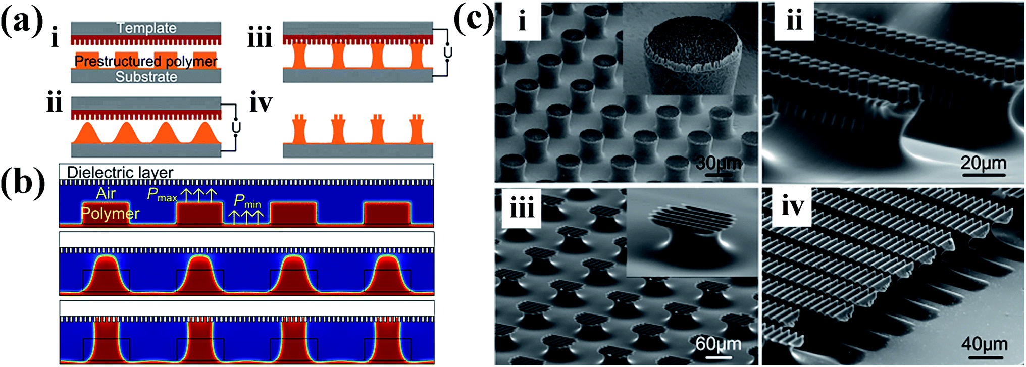 | ||
| Fig. 7 (a) Scheme and (b) numerical simulations of the process for generating hierarchical structures based on electrohydrodynamic (EHD) structure formation with a prestructured polymer. (c) Hierarchically structured polymer fabricated with different patterned template and prestructured polymer: (i) micropillar/nanopillar structure, (ii) micrograting/micropillar structure, (iii) micropillar/micrograting structure, and (iv) micrograting/micrograting structure. Reproduced with permission.124 Copyright 2016, American Chemical Society. | ||
Russel et al. design and utilize the special template patterns to guide pillars into alignment over regions much greater in extent than their natural domain sizes to pattern thin polymer films via EHDP, as shown in Fig. 8a–c. Regular rows of pillars form under ridges, and ordered triangular arrays are generated within each individual triangular domain bounded by the ridges, as shown in Fig. 8d. Moreover, the ordered pattern spanned more than 100 periods (400–500 μm), which is the largest array of ordered pillars from EHDP available in the literature. The ordered pattern had two identified characteristic wavelength: one is the spacing between pillars under the ridges, λ1 (∼2.7 μm), and the other is the spacing between pillars within each small triangular array, λ2 (∼4.0 μm), as shown in Fig. 8e–h.
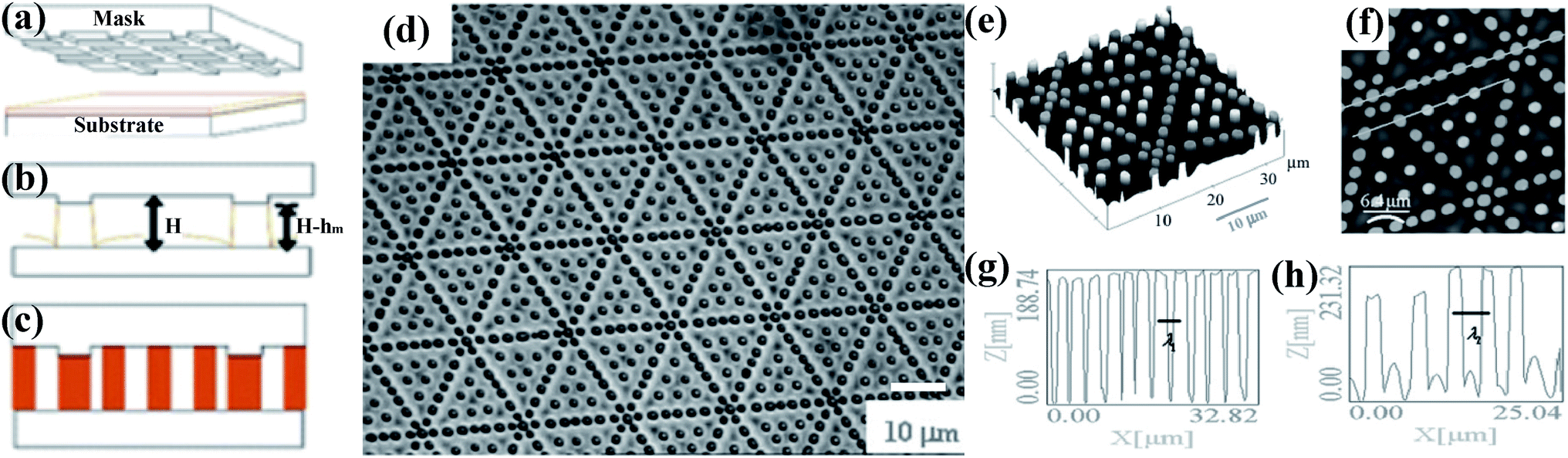 | ||
| Fig. 8 (a–c) The mechanism of the method used to align the pillars. (d) Optical microscopy images of a 45 nm thick PMMA film patterned on a silicon substrate. (e–h) AFM image of a typical pattern formed on the substrate with central pillars taller than those under the ridges. Reproduced with permission.126 Copyright 2006, WILEY-VCH. | ||
Li et al. presented an economical method for fabricating a concave microlens arrays (MLAs) with a high quality and high density, as shown in Fig. 9a and b.44 The curvature of the MLA can be well-controlled by changing the air gap between the template and polymer film. The MLA has a fill factor calculated as high as up to 93%, as shown in Fig. 9c. Moreover, the MLA has excellent focusing and imaging performances, as shown in Fig. 9d.
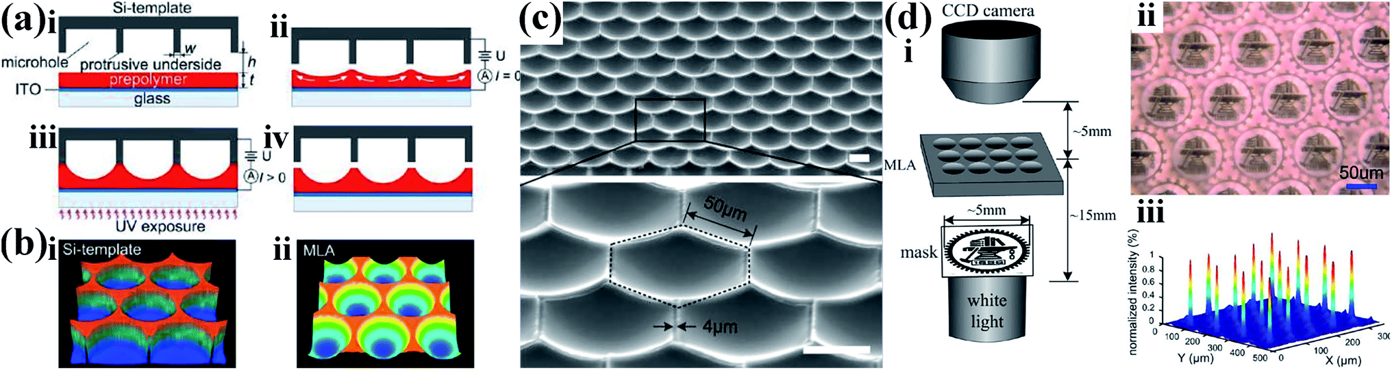 | ||
| Fig. 9 (a) Illustration of EHDP process for generation of concave MLAs. (b) Experimentally measured 3D profiles of (i) the template arrayed with cylindrical microholes and (ii) the corresponding concave MLA, respectively (acquired by LSCM). (c) SEM images of a concave MLA with a hexagonal aperture. Scale bar: 50 μm. (d) Test for the optical properties of concave MLA: (i) diagram of the optical microscopic setup to evaluate imaging and focusing performances of the MLA; (ii) image of the authors' school badge obtained by using a concave MLA with a sag height of ∼12 μm; (iii) measured light intensity profiles of a concave MLA with a sag height of ∼23 μm. Reproduced with permission.44 Copyright 2013, American Chemical Society. | ||
Sharma et al. showed that the spatiotemporal modulation of the applied electric field influences the pattern morphology in incompletely cross-linked viscoelastic polydimethylsiloxane (PDMS) films, due to the appearance of secondary and tertiary structures, resulting in hierarchical, multiscale patterns, which can be observed in Fig. 10.26 Park et al. also investigated secondary electrohydrodynamic instability in polymer films by controlling the timescale parameter to produce secondary nanosized patterns between the micrometer-sized grooves.127
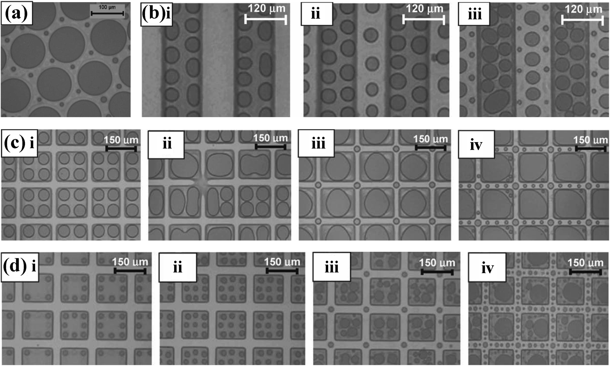 | ||
| Fig. 10 (a) Optical micrographs of EHDP under a top flat electrode using the spatiotemporal modulation of the applied electric field. (b) Optical micrographs of EHDP under a top electrode having parallel ridges and stripes of w = 120 μm using the spatiotemporal modulation of the applied electric field. (c) Optical micrographs of EHDP under a box-patterned top electrode using the spatiotemporal modulation of the applied electric field (box dimension ∼2λ). (d) Optical micrographs of EHDP under a box-patterned top electrode using the spatiotemporal modulation of the applied electric field (box dimension ∼3λ). Reproduced with permission.26 Copyright 2011, WILEY-VCH. | ||
Goldberg-Oppenheimer et al. proposed a tunable carbon nanotubes-based electrohydrodynamic patterning (CNT-EHDP) to fabricate unique multiscale structured cones and nanohair-like architectures with various periodicities and dimensions, successfully enabling surface energy minimization, as shown in Fig. 11.22 By controlling the hierarchy of micro- to nano cones and spikes, these morphologies provide a range of architectures with sufficient roughness for very low wettability, with the highest contact angle achieved of 173° and their properties can be easily switched between lotus-leaf to rose-petal behavior.
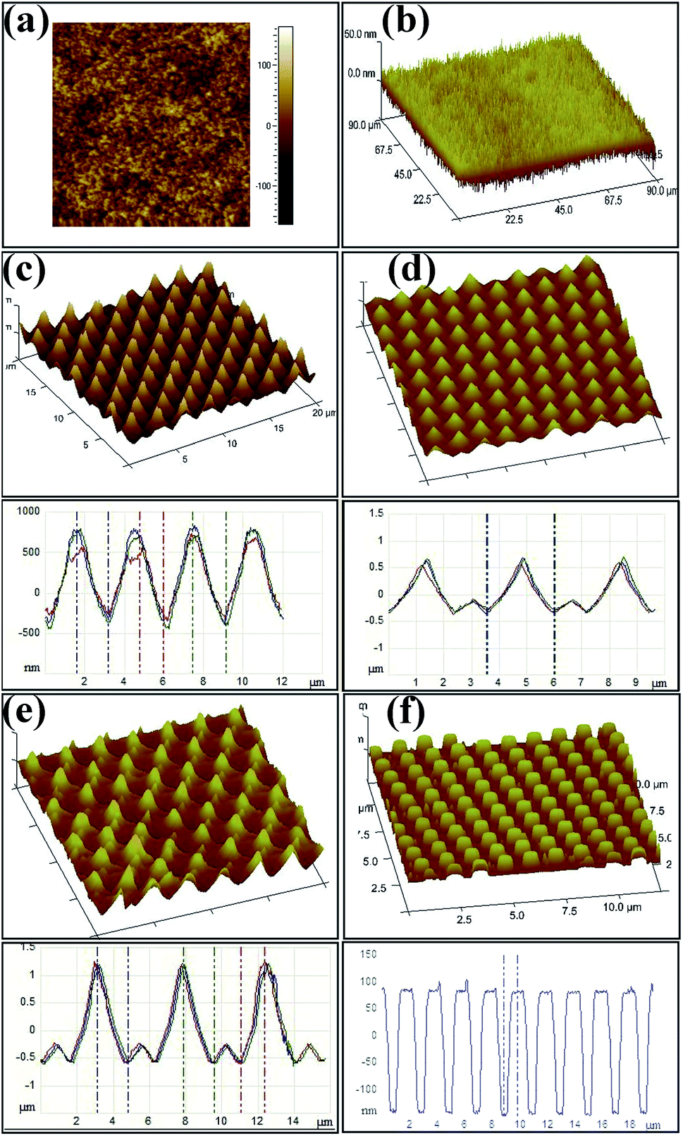 | ||
| Fig. 11 CNT-EHDP replicated patterns. Atomic force microscopy height and three-dimensional images and the corresponding cross-sections of (a) curly nano-hair (CNH) surfaces, (b) straight nano-hairs (SNH), (c) single-level spikes with rounded edges (S1L), (d) two-levelled spiky cones (S2L), (e) two-tiered heretical spiky cones (S2L2) and (f) hexagonal pillars (HP) replicated from the various imposed CNT-based electrodes. Reproduced with permission.22 Copyright 2017, Royal Society of Chemistry. | ||
6 Aligning and ordering of the anisotropic polymers
In order to take full advantage of the synergistic functions in carbon nanocomposites and hybrids, control of the dispersion, orientation, and interfacial chemistry of carbon materials in the organic or inorganic matrix is required. Moreover, anisotropic composite structures with vertically aligned carbon materials are essential to realize the full potential of carbon materials-based composites both for optimization of their mechanical properties and integration into devices. Goldberg-Oppenheimer et al. showed that the EHDP micro-patterns along with the alignment of carbon nanotubes (CNTs) within these patterns can be fabricated for carbon nanotube-polymer nanocomposite films by EHDP with a featureless template, as shown in Fig. 12a and b.128 The degree of the carbon nanotube alignment within these patterns can be tuned by adjusting the EHDP parameters. Furthermore, patterned surfaces decorated by CNT brushes can be obtained using either etching techniques or by embedding relatively long nanotubes, as shown in Fig. 12c.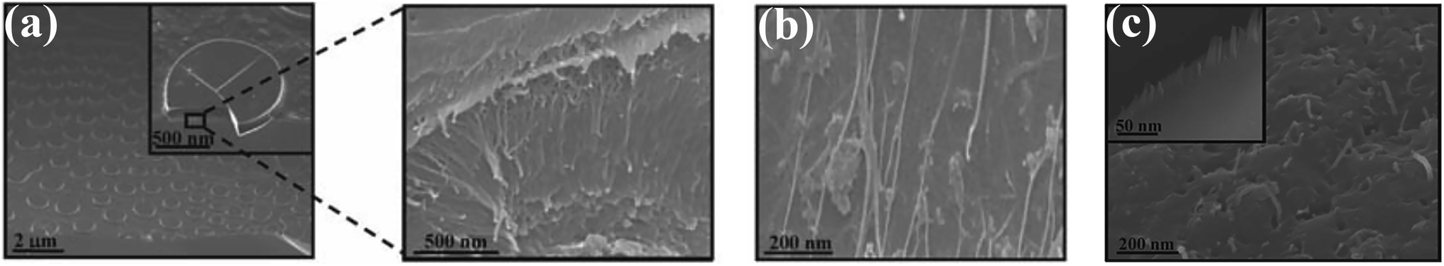 | ||
| Fig. 12 (a) Low- and high-magnification SEM images of the EHDP micro-pillars that contain vertically aligned MWCNTs. (b) SEM images of the EHDP micro-pillars with partial removal of the PS matrix. (c) SEM top-view of the EHDP micro-pillars with partially exposed vertical MWNTs. Inset: SEM images of the EHDP micro-pillars using CNTs which are slightly longer than the pillar height. Reproduced with permission.128 Copyright 2011, WILEY-VCH. | ||
EHDP enables the structure formation of organic crystalline materials on the micrometer length scale while at the same time exerting control over crystal orientation, as shown in Fig. 13.129 Well-ordered structures with nearly vertical walls, comprising stacks of crystals were shown for both PCL (Fig. 13a and b) and PDHA (Fig. 13e and f). A set of nested rings have formed in the diffraction plane for both replicated structures of PCL (Fig. 13c and d) and PDHA (Fig. 13g and h), indicating polycrystalline samples.
 | ||
| Fig. 13 AFM images of a (left) template electrode and (right) the patterns of (a) PCL and (e) PDHA with corresponding cross-sections. Optical micrographs of well-defined crystalline EHDP patterns of (b) PCL and of (f) PDHA. Diffraction patterns for a large area of (c) the PCL and (g) PDHA patterns. Selected area diffraction pattern obtained with an aperture of 3.0 μm of a single PCL crystal in (d) and with a 1.0 μm aperture diameter of a single PDHA crystal in (h). Reproduced with permission.129 Copyright 2012, WILEY-VCH. | ||
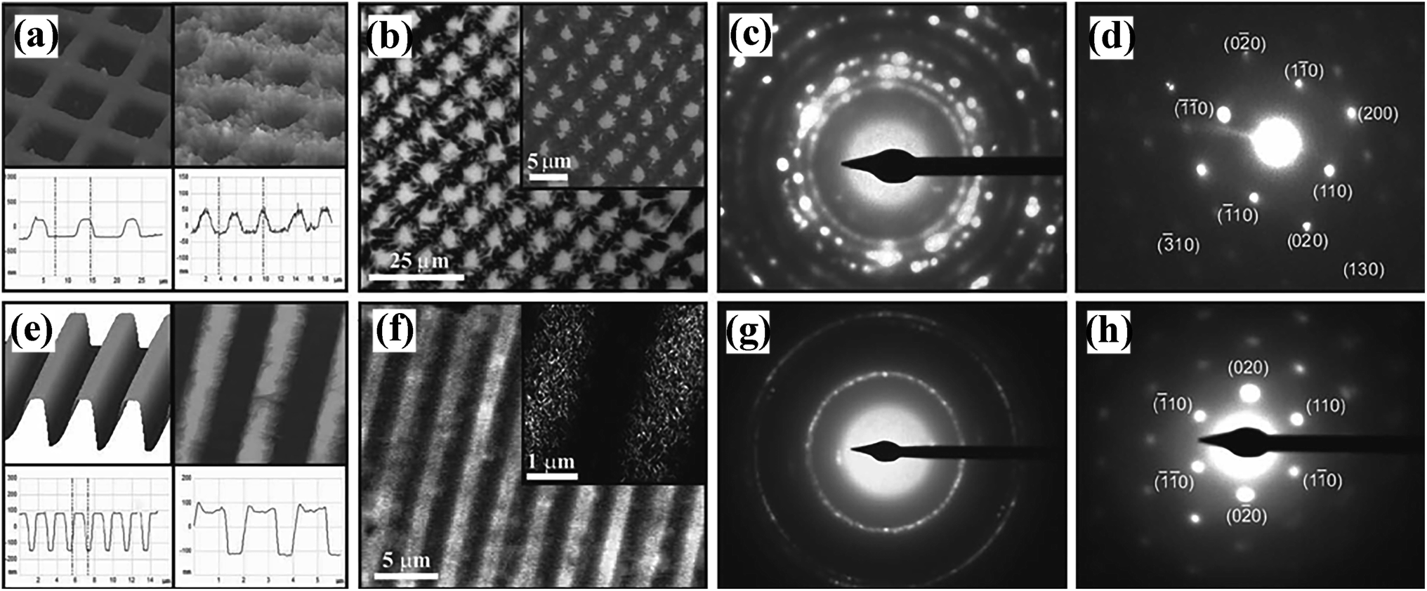
EHDP of a block-copolymer (BCP) film also gives rise to hierarchical pattern formation with a micrometer-sized polymer pillars and a 10 nm-scaled microphase morphology in one single step, as shown in Fig. 14.130–132 Schematic drawing of the experimental procedure was shown in Fig. 14a. The pattern formation on the micrometer scale of films with two different molecular weights was shown in Fig. 14c–e. The three different in-plane assemblies schematically was shown in Fig. 14b: onion-type concentric alignment of lamellae (Fig. 14f, arrow), parallel sheets (book sheets) (Fig. 14g) and bent lamellae pointing towards the column mantle (Fig. 14h and i). Furthermore, Goldberg-Oppenheimer et al. showed a functional block copolymer that contains perylene bismide (PBI) side chains which can crystallize via π–π stacking to form an electron conducting microphase is patterned via EHDP. The patterned film shows a hierarchical structure with three distinct length scales: micrometer-sized polymer pillars, a 10 nm BCP microphase morphology that is aligned perpendicular to the substrate surface, and a molecular length scale (0.35–3 nm) PBI π–π-stacks traverse the EHDP-generated plugs in a continuous fashion.133
 | ||
| Fig. 14 (a) Schematic drawing of the experimental procedure. (b) Three possible in-plane configurations of the lamellar microdomains. (c–e) AFM images of micrometer-sized patterns of PS-b-PMMA films made by EHD lithography. (f–i) SEM images of the microphase morphology of PS-b-PMMA columns. Reproduced with permission.131 Copyright 2008, WILEY-VCH. | ||
7 Conclusions and perspective
The review provides an illustrative commentary about the progress and recent developments on EHDP. The key emphasis of the review has been to theoretically and experimentally discuss how the characteristic wavelength and the characteristic time depend on both the external conditions (such as the applied voltage, film thickness, template-substrate spacing) and the initial polymer properties (such as rheological property, electrical property and surface tension). We have theoretically and experimentally discussed various possible strategies for fabricating hierarchical patterns by combining the essential concepts of bottom-up and top-down approaches. Furthermore, we have emphasized aligning and ordering of the anisotropic polymers by EHDP.Table 1 shows some conventional patterning methods and their characteristics of the resulting patterned surfaces including the cause, the pattern, the size range, the novelty and the limitation. Among the conventional patterning methods, photolithography is a pattern-fabricating technique with high resolution and high throughput, but the photolithography tools are rather expensive and the feature size is limited by optical diffraction limit; nanoimprint is a pattern-transferring technique with low cost, high throughput and high resolution, however, nanoimprint typically require a comparatively large external force to press a patterned template mechanically against the substrate, possibly leading to poor geometrical integrity in the duplicated structure or even to irreversible damage of the template and substrate, making multilayer overlay alignment difficult. EHDP also is a pattern-transferring technique with low cost, high throughput and high resolution. Moreover, the most major advantage of EHDP is the capability to fast and economically create large-scale three-dimensional micro-scale structures on various kinds of materials with featureless templates, even though no long range order and no nano-scale features due to the dielectric breakdown.71 In addition, EHDP just need a minimized external force to maintain a proper air gap between the liquid polymer and the template, avoiding the shortcoming of nanoimprint.
| Method | Cause | Pattern | Size range | Novelty | Limitation |
|---|---|---|---|---|---|
| Photolithography | Optical diffraction | Pattern of optical diffraction | Nanometer to micrometer | High resolution | High cost |
| High throughput | Optical diffraction limit | ||||
| Nanoimprint | External force | Typically negative replica of template | Nanometer to micrometer | Low cost | Large external force |
| High throughput | |||||
| High resolution | |||||
| EHDP | External electric field | Typically ordered arrays of pillars, positive replica of template or some hierarchical structures | Submicrometer to micrometer | Low cost | No long range order |
| High throughput | No nano-scale features | ||||
| High resolution | |||||
| Small external force |
A promising direction of EHDP is the conjugation with other patterning techniques (such as dewetting, nanoimprint, and hot embossing) to fabricate extremely high-aspect-ratio or hierarchical patterns such as, cages, microlens arrays, high-aspect-ratio micropillars, mushroom-shaped micropillars with a well-controlled aspect ratio and tip diameter.134–137 In addition, an attractive issue in EHDP is to extend its applicability to a larger class of materials. The benefit of exploiting new kinds of EHD materials lies in that it provides the possibility to not only improve the performance of EHDP, but also integrate functionality into final microstructures because of the interesting physical properties these materials can offer. So a promising direction in EHDP will include the structure formation in functional polymers and their various potential applications.
Conflicts of interest
The authors declare no competing financial interest.Acknowledgements
The research was financially supported by Natural Science Foundation of Shaanxi Province of China under Grant No. 2022JQ-485, Fundamental Research Funds for the Central Universities under Grant No. xjh012019034 and Natural Science Foundation of China (NSFC) under Grant No. 51473133.References
- Y.-K. Lai, Z. Chen and C.-J. Lin, Recent progress on the superhydrophobic surfaces with special adhesion: From natural to biomimetic to functional, J. Nanoeng. Nanomanuf., 2011, 1(1), 18–34 CrossRef CAS
.
- D. Chen, W. Zhao and T. P. Russell, P3ht nanopillars for organic photovoltaic devices nanoimprinted by aao templates, ACS Nano, 2012, 6(2), 1479–1485 CrossRef CAS PubMed
- L.-P. Wang, K.-Y. Yin, G. Li, Q. Liu, A.-X. Deng and H.-Y. Ma, Rhodamine b-loaded star polystyrenes and their luminescent honeycomb-patterned porous films, React. Funct. Polym., 2016, 99, 59–64 CrossRef CAS
- L. Li, K. Chen, L. Sun, S. Xie and S. Lin, Fabrication of patterned carbon nanotubes with adjustable arrays through controlled mesoscopic dewetting, React. Funct. Polym., 2013, 73(1), 83–88 CrossRef CAS
- M. R. Karim, J. H. Yeum, M. S. Lee and K. T. Lim, Preparation of conducting polyaniline/tio2 composite submicron-rods by the γ-radiolysis oxidative polymerization method, React. Funct. Polym., 2008, 68(9), 1371–1376 CrossRef CAS
- S. Y. Chou and L. Zhuang, Lithographically induced self-assembly of periodic polymer micropillar arrays, J. Vac. Sci. Technol., B, 1999, 17(6), 3197–3202 CrossRef CAS
- P. Deshpande and S. Y. Chou, Lithographically induced self-assembly of microstructures with a liquid-filled gap between the mask and polymer surface, J. Vac. Sci. Technol., B, 2001, 19(6), 2741–2744 CrossRef CAS
- P. Deshpande, X. Sun and S. Y. Chou, Observation of dynamic behavior of lithographically induced self-assembly of supramolecular periodic pillar arrays in a homopolymer film, Appl. Phys. Lett., 2001, 79(11), 1688–1690 CrossRef CAS
- S. Harkema, E. Schäffer, M. D. Morariu and U. Steiner, Pattern replication by confined dewetting, Langmuir, 2003, 19(23), 9714–9718 CrossRef CAS
- J. Peng, Y. Han, Y. Yang and B. Li, Pattern formation in polymer films under the mask, Polymer, 2003, 44, 2379–2384 CrossRef CAS
- L. Wu and S. Y. Chou, Dynamic modeling and scaling of nanostructure formation in the lithographically induced self-assembly and self-construction, Appl. Phys. Lett., 2003, 82(19), 3200–3202 CrossRef CAS
- L. Chen, L. Zhuang, P. Deshpande and S. Chou, Novel polymer patterns formed by lithographically induced self-assembly (lisa), Langmuir, 2005, 21, 818–821 CrossRef CAS PubMed
- L. Wu and S. Y. Chou, Electrohydrodynamic instability of a thin film of viscoelastic polymer underneath a lithographically manufactured mask, J. Non-Newtonian Fluid Mech., 2005, 125, 91–99 CrossRef CAS
- T.-C. Lin, L.-C. Huang, C.-C. Huang and C.-Y. Chao, Formation of self-assembled periodic groovesviathermal drawing lithography foe alignment layers in liquid crystal devices, Soft Matter, 2011, 7, 270–274 RSC
- E. Schaffer, T. Thurn-Albrecht, T. P. Russell and U. Steiner, Electrically induced structure formation and pattern transfer, Nature, 2000, 403(6772), 874–877 CrossRef CAS PubMed
- E. Schaffer, T. Thurn-Albrecht, T. P. Russell and U. Steiner, Electrohydrodynamic instabilities in polymer films, Europhys. Lett., 2001, 53(4), 518–524 CrossRef CAS
- L.-A. Turner, S. Downes, E. Hill and I. Kinloch, Investigating the suitability of electrohydrodynamic lithography for the fabrication of cell substrates, J. Mater. Sci., 2014, 49(11), 4045–4057 CrossRef CAS
- A. Kathalingam and H.-S. Kim, Electric field induced pattern formation on pmma and ito layers, Phys. Status Solidi A, 2018, 215(11), 1700811 CrossRef
- P. Goldberg-Oppenheimer and U. Steiner, Rapid electrohydrodynamic lithography using low-viscosity polymers, Small, 2010, 6(11), 1248–1254 CrossRef CAS PubMed
- P. T. Cheng, W. Zhou, F. Yang and S. Lee, Growth of polystyrene pillars in electric field, Langmuir, 2019, 35(14), 4966–4975 CrossRef CAS PubMed
- A. M. Koupaei, H. Nazaripoor and M. Sadrzadeh, Electrohydrodynamic patterning of polyethersulfone membranes, Langmuir, 2019, 35(37), 12139–12149 CrossRef CAS PubMed
- C. Busa, J. J. S. Rickard, E. Chun, Y. Chong, V. Navaratnam and P. Goldberg Oppenheimer, Tunable superapolar lotus-to-rose hierarchical nanosurfaces via vertical carbon nanotubes driven electrohydrodynamic lithography, Nanoscale, 2017, 9(4), 1625–1636 RSC
- N. Arun, A. Sharma, V. B. Shenoy and K. S. Narayan, Electric-field-controlled surface instabilities in soft elastic films, Adv. Mater., 2006, 18(5), 660–663 CrossRef CAS
- N. Arun, A. Sharma, P. S. Pattader, I. Banerjee, H. M. Dixit and K. S. Narayan, Electric-field-induced patterns in soft viscoelastic films: From long waves of viscous liquids to short waves of elastic solids, Phys. Rev. Lett., 2009, 102(25), 254502 CrossRef CAS PubMed
- A. J. Das and K. S. Narayan, Observation of bessel beams from electric-field-induced paterns on polymer surfaces, Opt. Lett., 2009, 34(21), 3391–3392 CrossRef CAS PubMed
- P. S. G. Pattader, I. Banerjee, A. Sharma and D. Bandyopadhyay, Multiscale pattern generation in viscoelastic polymer films by spatiotemporal modulation of electric field and control of rheology, Adv. Funct. Mater., 2011, 21(2), 324–335 CrossRef CAS
- C. H. Trease, P. J. S. Foot and A. T. Augousti, Electrohydrodynamic patterning in a curable resin over a wide range of fabrication parameters, Eur. Polym. J., 2017, 91, 315–325 CrossRef CAS
- K. Itoh, M. Ishida, Y. Kakinuma, H. Anzai and K. Sakirai, Development of an electro-adhesive micro pillar array via ehd patterning, Smart Mater. Struct., 2019, 28(3), 034003 CrossRef CAS
- K. A. Leach, Z. Lin and T. P. Russell, Early stages in the growth of electric field-induced surface fluctuations, Macromolecules, 2005, 38(11), 4868–4873 CrossRef CAS
- M. D. Dickey, E. Collister, A. Raines, P. Tsiartas, T. Holcombe, S. V. Sreenivasan, R. T. Bonnecaze and C. G. Willson, Photocurable pillar arrays formed via electrohydrodynamic instabilities, Chem. Mater., 2006, 18(8), 2043–2049 CrossRef CAS
- H. Tian, C. Wang, J. Shao, Y. Ding and X. Li, Electrohydrodynamic pressure enhanced by free space charge for electrically induced structure formation with high aspect ratio, Langmuir, 2014, 30(42), 12654–12663 CrossRef CAS PubMed
- G. Lv, S. Zhang, J. Shao, H. Tian, G. Wang and D. Yu, Preparation, properties, and efficient electrically induced structure formation of a leaky dielectric photoresist, RSC Adv., 2016, 6(85), 82450–82458 RSC
- G. Wang, G. Lv, S. Zhang, J. Shao, X. Li, H. Tian, D. Yu and L. Zhang, A photocurable leaky dielectric for highly electrical insulating electrohydrodynamic micro-/nanopatterns, Soft Matter, 2016, 12(43), 8819–8824 RSC
- G. Lv, S. Zhang, J. Shao, G. Wang, H. Tian and D. Yu, Rapid fabrication of electrohydrodynamic micro-/nanostructures with high aspect ratio using a leaky dielectric photoresist, React. Funct. Polym., 2017, 118, 1–9 CrossRef CAS
- N. E. Voicu, M. S. M. Saifullah, K. R. V. Subramanian, M. E. Welland and U. Steiner, Tio2 patterning using electro-hydrodynamic lithography, Soft Matter, 2007, 3(5), 554–557 RSC
- S. Cha, S. Lee, J. Eun Jang, A. Jang, J. Pyo Hong, J. Lee, J. Inn Sohn, D. Joon Kang and J. Min Kim, Ultrafast and low temperature laser annealing for crystalline tio2 nanostructures patterned by electro-hydrodynamic lithography, Appl. Phys. Lett., 2013, 103(5), 053114 CrossRef
- S. Lee, S. H. Jung, D. J. Kang and J. Lee, Fabrication of a nano-scale pattern with various functional materials using electrohydrodynamic lithography and functionalization, RSC Adv., 2016, 6(7), 5944–5948 RSC
- H. Chen, W. Yu, S. Cargill, M. K. Patel, C. Bailey, C. Tonry and M. P. Y. Desmulliez, Self-encapsulated hollow microstructures formed by electric field-assisted capillarity, Microfluid. Nanofluid., 2012, 13(1), 75–82 CrossRef
- G. Liu, W. Yu, H. Li, J. Gao, D. Flynn, R. W. Kay, S. Cargill, C. Tonry, M. K. Patel, C. Bailey and M. P. Y. Desmulliez, Microstructure formation in a thick polymer by electrostatic-induced lithography, J. Micromech. Microeng., 2013, 23(3), 035018 CrossRef CAS
- C. Tonry, M. K. Patel, C. Bailey, M. P. Y. Desmuliez, S. Cargill and W. Yu, A method for the micro-encapsulation of dielectric fluids in joined polymer shells, Curr. Org. Chem., 2013, 17(1), 65–71 CrossRef CAS
- S. Mahajan, T. Hutter, U. Steiner and P. Goldberg Oppenheimer, Tunable microstructured surface-enhanced raman scattering substrates via electrohydrodynamic lithography, J. Phys. Chem. Lett., 2013, 4(23), 4153–4159 CrossRef CAS
- S. Lee, S. Jung, A. R. Jang, J. Hwang, H. S. Shin, J. Lee and D. J. Kang, An innovative scheme for sub-50 nm patterning via electrohydrodynamic lithography, Nanoscale, 2017, 9(33), 11881–11887 RSC
- Y.-J. Lee, Y. W. Kim, Y.-K. Kim, C.-J. Yu, J. S. Gwag and J.-H. Kim, Microlens array fabricated using electrohydrodynamic instability and surface properties, Opt. Express, 2011, 19(11), 10673–10678 CrossRef CAS PubMed
- X. Li, H. Tian, Y. Ding, J. Shao and Y. Wei, Electrically templated dewetting of a uv-curable prepolymer film for the fabrication of a concave microlens array with well-defined curvature, ACS Appl. Mater. Interfaces, 2013, 5(20), 9975–9982 CrossRef CAS PubMed
- R. Li, L. Wang, H. Liu, W. Jiang, Y. Shi, L. Yin and Y. Zhu, Tunable mirolens array with a large fill-factor: Self-assembly fabrication and electrodrodynamic actuation, Sens. Actuators, A, 2016, 240, 85–91 CrossRef CAS
- S. Harkema and U. Steiner, Hierarchical pattern formation in thin polymer films using an electric field and vapor sorption, Adv. Funct. Mater., 2005, 15(12), 2016–2020 CrossRef CAS
- P. Lv, Y. You, J. Li, Y. Zhang, D. J. Broer, J. Chen, G. Zhou, W. Zhao and D. Liu, Translating 2d director profile to 3d topography in a liquid crystal polymer, Adv. Sci., 2021, 8(8), 2004749 CrossRef CAS PubMed
- N. Wu and W. B. Russel, Micro- and nano-patterns created via electrohydrodynamic instabilities, Nano Today, 2009, 4(2), 180–192 CrossRef CAS
- N. E. Voicu, S. Harkema and U. Steiner, Electric-field-induced pattern morphologies in thin liquid films, Adv. Funct. Mater., 2006, 16(7), 926–934 CrossRef CAS
- N. Wu, M. E. Kavousanakis and W. B. Russel, Coarsening in the electrohydrodynamic patterning of thin polymer films, Phys. Rev. E: Stat. Phys., Plasmas, Fluids, Relat. Interdiscip. Top., 2010, 81(2), 026306 CrossRef PubMed
- G. Amarandei, C. O'Dwyer, A. Arshak and D. Corcoran, Fractal patterning of nanoparticles on polymer films and their sers capabilities, ACS Appl. Mater. Interfaces, 2013, 5(17), 8655–8662 CrossRef CAS PubMed
- H. Tian, J. Shao, Y. Ding, X. Li and H. Liu, Numerical characterization of electrohydrodynamic micro- or nanopatterning processes based on a phase-field formulation of liquid dielectrophoresis, Langmuir, 2013, 29(15), 4703–4714 CrossRef CAS PubMed
- H. Tian, J. Shao, Y. Ding, X. Li and H. Liu, Simulation of polymer rheology in an electrically induced micro- or nano-structuring process based on electrohydrodynamics and conservative level set method, RSC Adv., 2014, 4(42), 21672 RSC
- X. Lei, L. Wu, P. Deshpande, Z. Yu, W. Wu, H. Ge and S. Y. Chou, 100 nm period gratings produced by lithographically induced self-construction, Nanotechnology, 2003, 14(7), 786–790 CrossRef CAS
- J. Heier, J. Groenewold and U. Steiner, Pattern formation in thin polymer films by spatially modulated electric fields, Soft Matter, 2009, 5(20), 3997 RSC
- T. Y. Hin, C. Liu, P. P. Conway, W. Yu, S. Cargill and M. P. Y. Desmulliez, Fabrication of a polymeric optical waveguide-on-flex using electrostatic-induced lithography, IEEE Photonics Technol. Lett., 2010, 22(13), 957–959 CAS
- X. Li, J. Y. Shao, Y. C. Ding, H. M. Tian and H. Z. Liu, Improving the height of replication in ehd patterning by optimizing the electrical properties of the template, J. Micromech. Microeng., 2011, 21(11), 115004 CrossRef
- H. M. Tian, Y. C. Ding, J. Y. Shao, X. M. Li and H. Z. Liu, Formation of irregular micro- or nano-structure with features of varying size by spatial fine-modulation of electric field, Soft Matter, 2013, 9(33), 8033–8040 RSC
- H. Tian, J. Shao, X. Chen, W. Jiang, L. Wang and Y. Ding, Investigation of the role of template features on the electrically induced structure formation (eisf) for a faithful duplication, Electrophoresis, 2017, 38(8), 1105–1112 CrossRef CAS PubMed
- H. Tian, J. Shao, Y. Ding, X. Li, X. Li and H. Liu, Influence of distorted electric field distribution on microstructure formation in the electrohydrodynamic patterning process, J. Vac. Sci. Technol., B: Nanotechnol. Microelectron.: Mater., Process., Meas., Phenom., 2011, 29(4), 041606 Search PubMed
- Q. Yang, B. Q. Li and Y. Ding, Dynamic modelling of micro/nano-patterning transfer by an electric field, RSC Adv., 2013, 3(46), 24658 RSC
- Q. Yang, B. Q. Li and Y. Ding, A numerical study of nanoscale electrohydrodynamic patterning in a liquid film, Soft Matter, 2013, 9(12), 3412 RSC
- Q. Yang, B. Q. Li, Y. Ding and J. Shao, Steady state of electrohydrodynamic patterning of micro/nanostructures on thin polymer films, Ind. Eng. Chem. Res., 2014, 53(32), 12720–12728 CrossRef CAS
- Q. Yang, B. Q. Li, H. Tian, X. Li, J. Shao, X. Chen and F. Xu, Deformation hysteresis of electrohydrodynamic patterning on a thin polymer film, ACS Appl. Mater. Interfaces, 2016, 8(27), 17668–17675 CrossRef CAS PubMed
- F. Boudoire, S. Partel, R. Toth and J. Heier, Combining parallel pattern generation of electrohydrodynamic lithography with serial addressing, RSC Adv., 2018, 8(54), 30932–30936 RSC
- P. Goldberg-Oppenheimer, Electrohydrodynamic patterning of functional materials, Doctoral thesis, The University of Cambridge, Springer Theses, 2013
- L. F. Pease III and W. B. Russel, Linear stability analysis of thin leaky dielectric films subjected to electric fields, J. Non-Newtonian Fluid Mech., 2002, 102(2), 233–250 CrossRef
- L. F. Pease III and W. B. Russel, Electrostatically induced submicron patterning of thin perfect and leaky dielectric films: A generalized linear stability analysis, J. Chem. Phys., 2003, 118(8), 3790–3803 CrossRef
- L. F. Pease III and W. B. Russel, Limitations on length scales for electrostatically induced submicrometer pillars and holes, Langmuir, 2004, 20(3), 795–804 CrossRef PubMed
- L. F. Pease III and W. B. Russel, Charge driven, electrohydrodynamic patterning of thin films, J. Chem. Phys., 2006, 125(18), 184716 CrossRef PubMed
- C. Y. Lau and W. B. Russel, Fundamental limitations on ordered electrohydrodynamic patterning, Macromolecules, 2011, 44(19), 7746–7751 CrossRef CAS
- J. Hwang, H. Park, J. Lee and D. J. Kang, Parametric scheme for rapid nanopattern replication via electrohydrodynamic instability, RSC Adv., 2021, 11(30), 18152–18161 RSC
- G. Tomar, V. Shankar, A. Sharma and G. Biswas, Electrohydrodynamic instability of a confined viscoelastic liquid film, J. Non-Newtonian Fluid Mech., 2007, 143(2–3), 120–130 CrossRef CAS
- J. Sarkar, A. Sharma and V. B. Shenoy, Electric-field induced instabilities and morphological phase transitions in soft elastic films, Phys. Rev. E: Stat. Phys., Plasmas, Fluids, Relat. Interdiscip. Top., 2008, 77(3 Pt 1), 031604 CrossRef PubMed
- P. Roy and P. S. Gooh Pattader, Electrohydrodynamic instability: Effect of rheological characteristics on the morphological evolution of liquid crystal–polymer interface, Bull. Mater. Sci., 2020, 43(1), 169 CrossRef CAS
- P. C. Tsiartas, M. D. Dickey, K. E. Allrich and C. G. Willson, Photocurable Pillar Arrays Formed via AC- and Ultrasound-Induced Electrohydrodynamic Instabilities, Proc. of SPIE, 2006, 6151, 61513G Search PubMed
- Z. Lin, T. Kerle, S. M. Baker, D. A. Hoagland, E. Schäffer, U. Steiner and T. P. Russell, Electric field induced instabilities at liquid/liquid interfaces, J. Chem. Phys., 2001, 114(5), 2377–2381 CrossRef CAS
- J. Bae, E. Glogowski, S. Gupta, W. Chen, T. Emrick and T. P. Russell, Effect of nanoparticles on the electrohydrodynamic instabilities of polymer/nanoparticle thin films, Macromolecules, 2008, 41(7), 2722–2726 CrossRef CAS
- Z. Lin, T. Kerle, T. P. Russell, E. Schaffer and U. Steiner, Structure formation at the interface of liquid/liquid bilayer in electric field, Macromolecules, 2002, 35(10), 3971–3976 CrossRef CAS
- D. H. Kho, S. H. Chae, U. Jeong, H. Y. Kim and J. K. Kim, Morphological development at the interface of polymer/polymer bilayer with an in situ compatibilizer under electric field, Macromolecules, 2005, 38(9), 3820–3827 CrossRef CAS
- R. M. Thaokar and V. Kumaran, Electrohydrodynamic instability of the interface between two fluids confined in a channel, Phys. Fluids, 2005, 17(8), 084104 CrossRef
- N. Wu and W. B. Russel, Electrohydrodynamic instability of dielectric bilayers: Kinetics and thermodynamics, Ind. Eng. Chem. Res., 2006, 45(16), 5455–5465 CrossRef CAS
- K. John, P. Hänggi and U. Thiele, Ratchet-driven fluid transport in bounded two-layer films of immiscible liquids, Soft Matter, 2008, 4(6), 1183 RSC
- A. K. Uguz, O. Ozen and N. Aubry, Electric field effect on a two-fluid interface instability in channel flow for fast electric times, Phys. Fluids, 2008, 20(3), 031702 CrossRef
- P. Gambhire and R. M. Thaokar, Linear stability analysis of electrohydrodynamic instabilities at fluid interfaces in the “small feature” limit, Eur. Phys. J. E, 2011, 34(8), 84 CrossRef CAS PubMed
- J. Bae, Electrohydrodynamic instabilities of polymer thin films: Filler effect, J. Ind. Eng. Chem., 2012, 18(1), 378–383 CrossRef CAS
- P. Gambhire and R. M. Thaokar, Role of conductivity in the electrohydrodynamic patterning of air-liquid interfaces, Phys. Rev. E: Stat., Nonlinear, Soft Matter Phys., 2012, 86(3 Pt 2), 036301 CrossRef CAS PubMed
- H. Nazaripoor, C. R. Koch, M. Sadrzadeh and S. Bhattacharjee, Electrohydrodynamic patterning of ultra-thin ionic liquid films, Soft Matter, 2015, 11(11), 2193–2202 RSC
- H. Nazaripoor, C. R. Koch, M. Sadrzadeh and S. Bhattacharjee, Compact micro/nano electrohydrodynamic patterning: Using a thin conductive film and a patterned template, Soft Matter, 2016, 12(4), 1074–1084 RSC
- K. Mondal and D. Bandyopadhyay, Electro-capillary instabilities of thin leaky elastic-viscous bilayers, Phys. Fluids, 2014, 26(12), 122006 CrossRef
- H. Nazaripoor, C. R. Koch and S. Bhattacharjee, Electrical perturbations of ultrathin bilayers: Role of ionic conductive layer, Langmuir, 2014, 30(49), 14734–14744 CrossRef CAS PubMed
- V. Shankar and A. Sharma, Instability of the interface between thin fluid films subjected to electric fields, J. Colloid Interface Sci., 2004, 274(1), 294–308 CrossRef CAS PubMed
- L. Jiang, X. Wang and L. Chi, Nanoscaled surface patterning of conducting polymers, Small, 2011, 7(10), 1309–1321 CrossRef CAS PubMed
- J. Z. Wang, Z. H. Zheng, H. W. Li, W. T. Huck and H. Sirringhaus, Dewetting of conducting polymer inkjet droplets on patterned surfaces, Nat. Mater., 2004, 3(3), 171–176 CrossRef CAS PubMed
- L. Li, M. Hirtz, W. Wang, C. Du, H. Fuchs and L. Chi, Patterning of polymer electrodes by nanoscratching, Adv. Mater., 2010, 22(12), 1374–1378 CrossRef CAS PubMed
- B. H. Kim, M. S. Onses, J. B. Lim, S. Nam, N. Oh, H. Kim, K. J. Yu, J. W. Lee, J. H. Kim, S. K. Kang, C. H. Lee, J. Lee, J. H. Shin, N. H. Kim, C. Leal, M. Shim and J. A. Rogers, High-resolution patterns of quantum dots formed by electrohydrodynamic jet printing for light-emitting diodes, Nano Lett., 2015, 15(2), 969–973 CrossRef CAS PubMed
- J. Huang, S. Virji, B. H. Weiller and R. B. Kaner, Polyaniline nanofibers: Facile synthesis and chemical sensors, J. Am. Chem. Soc., 2003, 125(2), 314–315 CrossRef CAS PubMed
- H. Liu, J. Kameoka, D. A. Czaplewski and H. G. Craighead, Polymeric nanowire chemical sensor, Nano Lett., 2004, 4(4), 671–675 CrossRef CAS
- B. Dong, D. Y. Zhong, L. F. Chi and H. Fuchs, Patterning of conducting polymers based on a random copolymer strategy: Toward the facile fabrication of nanosensors exclusively based on polymers, Adv. Mater., 2005, 17(22), 2736–2741 CrossRef CAS
- J. J. Rickard, I. Farrer and P. Goldberg Oppenheimer, Tunable nanopatterning of conductive polymers via electrohydrodynamic lithography, ACS Nano, 2016, 10(3), 3865–3870 CrossRef CAS PubMed
- S. Manigandan, S. Majumder, A. Suresh, S. Ganguly, K. Kargupta and D. Banerjee, Electric field induced dewetting and pattern formation in thin conducting polymer film, Sens. Actuators, B, 2010, 144(1), 170–175 CrossRef CAS
- Z. Ye, H. Cui, X. Yang and F. Qiu, Charge injection promoted electrohydrodynamic instabilities in poly(3-hexylthiophene) thin films, J. Mater. Chem. C, 2015, 3(9), 1949–1956 RSC
- M. D. Morariu, N. E. Voicu, E. Schaffer, Z. Lin, T. P. Russell and U. Steiner, Hierarchical structure formation and pattern replication induced by an electric field, Nat. Mater., 2003, 2(1), 48–52 CrossRef CAS PubMed
- K. A. Leach, S. Gupta, M. D. Dickey, C. G. Willson and T. P. Russell, Electric field and dewetting induced hierarchical structure formation in polymer/polymer/air trilayers, Chaos, 2005, 15(4), 047506 CrossRef PubMed
- M. D. Dickey, S. Gupta, K. A. Leach, E. Collister, C. G. Willson and T. P. Russell, Novel 3-d structures in polymer films by coupling external and internal fields, Langmuir, 2006, 22(9), 4315–4318 CrossRef CAS PubMed
- P. Goldberg-Oppenheimer, S. Mahajan and U. Steiner, Hierarchical electrohydrodynamic structures for surface-enhanced raman scattering, Adv. Mater., 2012, 24(23), OP175–OP180 CAS
- P. D. S. Reddy, D. Bandyopadhyay and A. Sharma, Self-organized ordered arrays of core-shell columns in viscous bilayers formed by spatially varying electric fields, J. Phys. Chem. C, 2010, 114(49), 21020–21028 CrossRef CAS
- P. D. S. Reddy, D. Bandyopadhyay and A. Sharma, Electric-field-induced instabilities in thin liquid trilayers confined between patterned electrodes, J. Phys. Chem. C, 2012, 116(43), 22847–22858 CrossRef CAS
- D. Bandyopadhyay, A. Sharma, U. Thiele and P. D. Reddy, Electric-field-induced interfacial instabilities and morphologies of thin viscous and elastic bilayers, Langmuir, 2009, 25(16), 9108–9118 CrossRef CAS PubMed
- S. A. Roberts and S. Kumar, Electrohydrodynamic instabilities in thin liquid trilayer films, Phys. Fluids, 2010, 22(12), 122102 CrossRef
- D. Bandyopadhyay, P. Dinesh Sankar Reddy and A. Sharma, Electric field and van der waals force induced instabilities in thin viscoelastic bilayers, Phys. Fluids, 2012, 24(7), 074106 CrossRef
- K. Mondal, P. Kumar and D. Bandyopadhyay, Electric field induced instabilities of thin leaky bilayers pathways to uniyue morphologies and miniaturization, J. Chem. Phys., 2013, 138, 024705 CrossRef PubMed
- M. D. Dickey, A. Raines, E. Collister, R. T. Bonnecaze, S. V. Sreenivasan and C. G. Willson, High-aspect ratio polymeric pillar arrays formed via electrohydrodynamic patterning, J. Mater. Sci., 2008, 43(1), 117–122 CrossRef CAS
- H. M. Tian, J. Y. Shao, Y. C. Ding, X. M. Li and H. Hu, Electrohydrodynamic micro-/nanostructuring processes based on prepatterned polymer and prepatterned template, Macromolecules, 2014, 47(4), 1433–1438 CrossRef CAS
- H. Hu, H. Tian, X. Li, J. Shao, Y. Ding, H. Liu and N. An, Biomimetic mushroom-shaped microfibers for dry adhesives by electrically induced polymer deformation, ACS Appl. Mater. Interfaces, 2014, 6(16), 14167–14173 CrossRef CAS PubMed
- X. Chen, H. Tian, X. Li, J. Shao, Y. Ding, N. An and Y. Zhou, A high performance p(vdf-trfe) nanogenerator with self-connected and vertically integrated fibers by patterned ehd pulling, Nanoscale, 2015, 7(27), 11536–11544 RSC
- X. Chen, J. Shao, X. Li and H. Tian, A flexible piezoelectric-pyroelectric hybrid nanogenerator based on p(vdf-trfe) nanowire array, IEEE Trans. Nanotechnol., 2016, 15(2), 295–302 CAS
- H. Hu, J. Shao, H. Tian, X. Li and C. Jiang, Mushroom-shaped micropillars for robust nonwetting surface by electrohydrodynamic structuring technique, IEEE Trans. Nanotechnol., 2016, 15(2), 237–242 CAS
- G. Lv, Y. Liu, J. Shao, H. Tian and D. Yu, Facile fabrication of electrohydrodynamic micro-/nanostructures with high aspect ratio of a conducting polymer for large-scale superhydrophilic/superhydrophobic surfaces, Macromol. Mater. Eng., 2018, 303(2), 1700361 CrossRef
- H. Tian, J. Shao, X. Chen, L. Wang and Y. Ding, A versatile approach to fabricate modulated micro-/nanostructures by electrohydrodynamic structuring on prepatterned polymer, J. Micromech. Microeng., 2017, 27(2), 025008 CrossRef
- G. Lv, H. Tian, J. Shao and D. Yu, Synthesis, characterization, and efficient electrohydrodynamic patterning with a high aspect ratio of a soluble oligomerpyrrole derivative, React. Funct. Polym., 2019, 137, 116–122 CrossRef CAS
- H. Tian, J. Shao, H. Hu, L. Wang and Y. Ding, Role of space charges inside a dielectric polymer in the electrohydrodynamic structure formation on a prepatterned polymer (esf-pp), RSC Adv., 2016, 6(81), 77275–77283 RSC
- H. Hu, H. Tian, J. Shao, Y. Ding, C. Jiang and H. Liu, Fabrication of bifocal microlens arrays based on controlled electrohydrodynamic reflowing of pre-patterned polymer, J. Micromech. Microeng., 2014, 24(9), 095027 CrossRef CAS
- H. Tian, J. Shao, H. Hu, L. Wang and Y. Ding, Generation of hierarchically ordered structures on a polymer film by electrohydrodynamic structure formation, ACS Appl. Mater. Interfaces, 2016, 8(25), 16419–16427 CrossRef CAS PubMed
- G. Lv, X. Hu, L. Hao, H. Tian, J. Shao and D. Yu, Facile fabrication of a flexible patterned film with diverse micro-/nanostructures via electrohydrodynamic patterning, Ind. Eng. Chem. Res., 2021, 60(1), 314–323 CrossRef CAS
- N. Wu, L. F. Pease and W. B. Russel, Toward large-scale alignment of electrohydrodynamic patterning of thin polymer films, Adv. Funct. Mater., 2006, 16(15), 1992–1999 CrossRef CAS
- H. Park, J. Hwang, T. H. Lee, J. Lee and D. J. Kang, Fog collection based on secondary electrohydrodynamic-induced hybrid structures with anisotropic hydrophilicity, ACS Appl. Mater. Interfaces, 2021, 13(23), 27575–27585 CrossRef CAS PubMed
- P. Goldberg-Oppenheimer, D. Eder and U. Steiner, Carbon nanotube alignment via electrohydrodynamic patterning of nanocomposites, Adv. Funct. Mater., 2011, 21(10), 1895–1901 CrossRef CAS
- P. Goldberg-Oppenheimer, P. Kohn, R. M. Langford and U. Steiner, Patterning of crystalline organic materials by electro-hydrodynamic lithography, Small, 2012, 8(16), 2595–2601 CrossRef CAS PubMed
- H. Xiang, Y. Lin and T. P. Russell, Electrically induced patterning in block copolymer films, Macromolecules, 2004, 37(14), 5358–5363 CrossRef CAS
- N. E. Voicu, S. Ludwigs and U. Steiner, Alignment of lamellar block copolymers via electrohydrodynamic-driven micropatterning, Adv. Mater., 2008, 20(16), 3022–3027 CrossRef CAS
- Y. Zhou, A. Nicolas, K. R. Thomas and U. Steiner, Interplay of electrohydrodynamic structure formation and microphase alignment in lamellar block copolymers, Soft Matter, 2012, 8(14), 3841–3847 RSC
- P. Goldberg-Oppenheimer, D. Kabra, S. Vignolini, S. Hüttner, M. Sommer, K. Neumann, M. Thelakkat and U. Steiner, Hierarchical orientation of crystallinity by block-copolymer patterning and alignment in an electric field, Chem. Mater., 2013, 25(7), 1063–1070 CrossRef CAS
- S. H. Lee, P. Kim, H. E. Jeong and K. Y. Suh, Electrically induced formation of uncapped, hollow polymeric microstructures, J. Micromech. Microeng., 2006, 16(11), 2292–2297 CrossRef CAS
- S. Dwivedi, Vivek, R. Mukherjee and A. Atta, Formation and control of secondary nanostructures in electro-hydrodynamic patterning of ultra-thin films, Thin Solid Films, 2017, 642, 241–251 CrossRef CAS
- S. Dwivedi, R. Narayanan, R. Chaudhary, R. Mukherjee and A. Atta, Controlled nanoscale electrohydrodynamic patterning using mesopatterned template, ACS Omega, 2018, 3(8), 9781–9789 CrossRef CAS PubMed
- H. Li, W. Yu, Y. Wang, H. Bu, Z. Liu, E. Abraham and M. P. Y. Desmulliez, Simulation of the electrohydrodynamic instability process used in the fabrication of hierarchic and hollow micro/nanostructures, RSC Adv., 2014, 4(27), 13774 RSC
| This journal is © The Royal Society of Chemistry 2022 |