
 Open Access Article
 This Open Access Article is licensed under a Creative Commons Attribution-Non Commercial 3.0 Unported Licence
High performance enhancement-mode thin-film transistor with graphene quantum dot-decorated In2O3 channel layers
Xiaofen Xua,
Gang He *a,
Shanshan Jiang*b,
Leini Wanga,
Wenhao Wanga,
Yanmei Liua and
Qian Gao*a
*a,
Shanshan Jiang*b,
Leini Wanga,
Wenhao Wanga,
Yanmei Liua and
Qian Gao*a
aSchool of Materials Science and Engineering, Anhui University, Hefei 230601, China
bSchool of Integration Circuits, Anhui University, Hefei 230601, China. E-mail: hegang@ahu.edu.cn; jiangshanshan@ahu.edu.cn; gaoq@ahu.edu.cn
First published on 18th May 2022
Abstract
Due to the quantum confinement and edge effects, there has been ongoing enthusiasm to provide deep insight into graphene quantum dots (GQDs), serving as attractive semiconductor materials. To demonstrate the potential applications of GQDs in electronic devices, this work presents solution-processed high performance GQD-decorated In2O3 thin-film transistors (TFTs) based on ZrO2 as gate dielectrics. GQDs-In2O3/ZrO2 TFTs with optimized doping content have demonstrated high electrical performance and low operating voltage, including a larger field-effect mobility (μFE) of 34.02 cm2 V−1 s−1, a higher Ion/Ioff of 4.55 × 10⁷, a smaller subthreshold swing (SS) of 0.08 V dec−1, a lower interfacial trap states (Dit) of 5.84 × 1011 cm−2 and threshold voltage shift of 0.07 V and 0.12 V under positive bias stress (PBS) and negative bias stress (NBS) for 3600 s, respectively. As a demonstration of complex logic applications, a resistor-loaded unipolar inverter based on GQDs-In2O3/ZrO2 has been built, demonstrating full swing characteristic and high gain of 10.63. Low-frequency noise (LFN) characteristics of GQDs-In2O3/ZrO2 TFTs have been presented and it was concluded that the noise source can be attributed to the fluctuations in mobility. As a result, it can be concluded that solution-derived GDQ-optimized oxide-based TFTs will manifest potential applications in electronic devices.
Introduction
Graphene quantum dots (GQDs) are derivatives of graphene with nanometer size, and have common characteristics of graphene and quantum dots.1 They have a non-zero bandgap because of quantum confinement,2 resulting in their unique properties such as large surface area, excellent solubility, edge effects etc.3–5 As a result, GQDs are becoming promising semiconductor nanomaterials for applications in biological imaging,6 ultrasensitive sensors,7 supercapacitors,8,9 and electronic and opto-electronic devices.3,10–13In2O3, a representative of transparent n-type semiconductors with a wide band gap of 3.6 eV, is one of the most widely used materials in various fields ranging from optoelectronic devices to thin film transistors (TFTs) due to its lower processing temperature, environment friendliness and good optoelectronic properties.14–16 Due to its potential application in next-generation display devices, In2O3-based oxide TFTs have attracted more attention.17–19 Even though the attracting properties of In2O3 TFTs, but there exist too much oxygen vacancies (VO) in In2O3 thin films, leading to the more formation of more electrons and the deteriorated devices performance.20 It has reported that VO-related defects and superabundant mobile electrons will result in higher off-current (Ioff) and poor bias stress stability.19,21
With the aim of improving the electrical stability, great progress has been made in incorporating carrier suppressor dopants into the channel layers of the In2O3-based TFTs. To date, In2O3 films doped by gallium,22 zinc,23 tin,24 yttrium,25 and magnesium26 have been achieved to optimize the TFTs performance. However, their preparations and applications are limited because these doped elements are usually scarce and toxicant. Due to their unique electron transport properties, GQDs may play a key role in In2O3-based TFTs devices.11 Based on Shan's investigation, it can be noted that TFTs modified by GQDs are desirable.27,28 In spite of the attractive electrical properties, the performance improvement mechanism of GQDs decorated In2O3-based TFTs is still unclear and requires further study. Therefore, based on the research perspective and further technology application, developing an effective and simple method to prepare GQDs-decorated TFTs is urgently needed. Up to now, various methods have been adopted to fabricate oxide-based TFTs, such as atomic layer deposition (ALD) and sputtering, which highly depend on vacuum-based ambient. What's more, the complicated process and high costs of fabrication inhibit its potential application. By contrast, solution-based process has been paid more attention due to its advantages, including easy operation, low cost, easy controllability, and large-scale productivity. Therefore, great efforts have been made in preparing solution-driven oxide TFTs devices.29–31
In this work, based on a solution-based route, a simple and feasible way has been pursued to synthesize GQDs-decorated In2O3 thin films. Furthermore, a systematical investigation was conducted to reveal the variation in microstructure and component of GQDs-decorated In2O3 films with different doping level. To demonstrate the potential possibility of GQDs in CMOS logics, their applications in GQD-In2O3 TFTs and resistor-loaded inverters based on solution-processed ZrOx gate dielectrics by device engineering were also demonstrated, and then evaluated carefully. Experiment results have revealed that the optimized GQD-In2O3 TFTs and resistor-loaded inverter with full swing characteristics have been achieved. The improvement in performance of In2O3-based TFTs by GQDs doping engineering has been discussed in detail.
Experimental
GQDs were synthesized by our reported method.32 The p-type heavily doped Si wafers were chosen as the substrates. Firstly, 0.1 M In2O3 and 0.1 M ZrOx solution was obtained by dissolving 0.3 g In(NO3)3·xH2O (99%) and 0.64 g ZrOCl2·8H2O (99%) in 10 mL 2-methoxyethanol (2-ME). Meanwhile, 1 mg, 2 mg and 3 mg GQDs were mixed with the In2O3 precursor solution, respectively. All the solution were subjected to 8 hour agitation and 12 hour aging. Then, the ZrOx precursor solution was spun thrice on the Si wafers under speed of 4500 rpm and baked at 200 °C for 10 min. After UV treatment for 30 min, the as-deposited films experienced 600 °C annealing treatment for 2 h. Moreover, the pure In2O3 and GQDs-decorated In2O3 precursor solution was spun once on the ZrOx dielectric layer under speed of 2500 rpm and baked at 150 for 10 min, respectively. The samples were annealed at 280 °C in air ambient for 1 h. Finally, 100 nm thick Al thin film was deposited by thermal evaporation to form source and drain electrodes by a shadow mask with width of 1000 μm and length of 200 μm. TFTs with pure In2O3 channel layer were fabricated in the same way. For convenience, the corresponding samples were denoted as GQDs-In2O3-1, GQDs-In2O3-2, and GQDs-In2O3-3 with the concentration of GQDs of 0.1 mg ml−1, 0.2 mg ml−1, and 0.3 mg ml−1, respectively. The crystal structures of GQDs-In2O3 and In2O3 thin films spin-coated on Si substrates were investigated by X-ray diffractometer (XRD, Empyrean S3, Netherlands) with a Cu Kα radiation. The surface morphologies of the thin films were investigated by atomic force microscopy (AFM, 5500M, Hitachi, Japan). X-ray photoelectron spectroscopy (XPS) analyses were carried out by using ESCALAB 250Xi system (Thermo Fisher Scientific, USA) with Al Kα radiation (1486.6 eV). To study the thermal behavior of the precursor solution in air, a thermogravimetric analyzer (TGA, STA449F3) was carried out at a heating rate of 10 °C min−1. The UV visible spectroscopy (UV-Vis-2550, Shimadzu) was used to measure the optical properties of GQDs-In2O3 and In2O3 thin films spin-coated on quartz substrates. The cross-sectional images of the GQDs-In2O3 TFT device were obtained using transmission electron microscope (TEM, JEOL-F200). The electrical performances of the integrated TFTs and resistor-loaded unipolar inverter were measured under an air ambient by a semiconductor parameter analyzer (Agilent B1500A and Keithley 2636B) in a dark box. The low frequency noise (LFN) characteristics of the GQDs-In2O3 and In2O3 TFTs was detected by semiconductor parameter analyzer (PDA FS-380). The field-effect mobility (μFE) of the TFTs was calculated by the following formula:
 | (1) |
 | (2) |
Results and discussion
To investigate the thermal behavior of In2O3 precursor powders with different GQDs dopingo concentrations, corresponding measurements were performed using TGA under nitrogen ambient conditions, and the result is depicted in Fig. 1. As shown in Fig. 1(a), three steps of weight loss occurring from 50 °C to 390 °C have been observed. The first step of weight loss from 50 °C to 150 °C can be attributed to the evaporation of the residual solvent from the precursor powder.33 The second weight loss occurs between 150 °C and 260 °C, In(NO3)3 starts to decompose and turn into In(OH)3, indicating the decomposition, hydrothermal, and the thermal dihydroxylation reaction of In(NO3)3. According to the previous reports, it can be noted that In(OH)3 can be transformed into orthorhombic InOOH with metatable state, an intermediate product. It is worth noting that the weight decreases abruptly between 260 °C to 390 °C. This stage represents the dehydroxylation and thermal decomposition of the intermediate products of InOOH, leading to the formation of In2O3. After 390 °C, no evident change in the weight loss has been detected, indicating that the In2O3 thin films are almost completely formed. Current observations is in good agreement with previous reports that crystallization of the In2O3 can be ultimately achieved above 390 °C.34,35 After doping by GQDs, the reduction in the transfer temperature has been found, suggesting that GQDs doping can reduce the temperature of In2O3 film preparation. This is consistent with previous reports that graphene-like materials are accompanied by strong gas release, resulting in rapid thermal expansion.36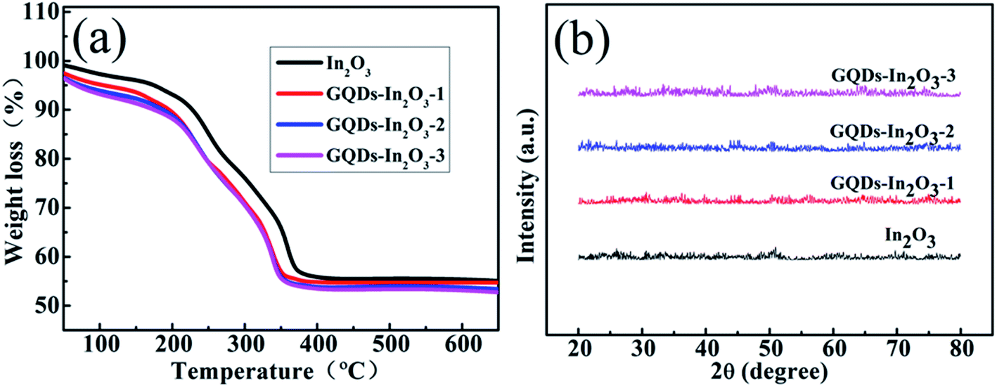 | ||
| Fig. 1 (a) Thermal behavior of the pure In2O3 and GQDs-In2O3 precursor powders. (b) XRD patterns of the In2O3 and GQDs-In2O3 thin films. | ||
As depicted in Fig. 1(b), the variation in the microstructure of In2O3thin films with different GQDs doping concentrations was investigated by XRD. No characteristic peaks of In2O3 and GQDs-In2O3 thin films are observed, regardless of the GQDs doping concentrations, meaning that all the films are in an amorphous state. It is well known that the amorphous films have the advantage of large area uniformity, smooth surface, high stability, low interfacial state density, which are very beneficial to improve the performance of TFT devices.37
To verify the potential application of In2O3 and GQDs-In2O3 thin films in the field of transparent electronic devices, the all the films spin-coated on quartz substrates were measured by UV-Vis. As depicted in Fig. 2(a), it can be seen that all the thin films are highly transparent with an average optical transmittance of over 90% in the visible range, demonstrating its feasibility in transparent electronic devices. In addition, the transmittance of the GQDs-In2O3 samples increases slightly as the GQDs concentration increases, which can be attributed to the strong photoluminescence of GQDs.38,39 Based on Tauc plot method, the optical bandgap for the GQDs-In2O3 thin films as a function of GQDs doping concentrations were determined and displayed in Fig. 2(b). Based on Fig. 2(b), it can be seen that the bandgap of In2O3 thin films increases from 3.77 eV to 4.15 eV with GQDs content increasing. As reported, the increased bandgap after GQDs doping is associated with the decreased grain size of thin films and the bund gap of GQDs due to its quantum confinement.2,40,41
 | ||
| Fig. 2 (a) Optical transmittance and (b) bandgap of In2O3 thin films with different GQDs concentrations. | ||
To understand the evolution of the chemical bonding states of In2O3 thin film as function of GQDs doping concentrations, XPS measurements were carried out and displayed in Fig. 3. All the XPS spectra deconvolution was performed by Shirley background subtraction using a Voigt function convoluting Gaussian and Lorentzian functions. Fig. 3(a) shows the O 1s XPS spectra for the In2O3 and GQDs-In2O3 samples and the binding energies of the O 1s peaks are deconvoluted into three subpeaks centered at 529.9, 531, and 531.8 eV, which can be assigned to the oxygen in oxide lattice (M–O), the oxygen in oxygen vacancies (VO), and the oxygen in hydroxyl species (M–OH), respectively.42,43 Compared with In2O3 sample, the XPS feature of GQDs-In2O3 samples shifts toward the higher binding energy due to the M–OH oxygen atoms are less negatively charged than those in oxides.44 Based on the XPS results, the fraction of oxygen-related components in In2O3 and GQDs-In2O3 samples was quantitatively discussed and illustrated in Fig. 3(b). It is noteworthy that with increasing GQDs concentration from 0 to 0.3 mg ml−1, the fraction of M–O contents increased from 40.0% to 48% and the fraction of M–OH species from 33% to 27% have been observed, which indicates that GQDs doping helps to convert the M–OH to M–O content. The VO composition increases from 27% to 28% and then decreases to 25%. This phenomenon is caused by insufficient GQDs element incorporated into In2O3, so there is not enough GQDs to inhibit the oxygen vacancy caused by In2O3. Which is consistent with our previous investigations.33 Fig. 3(c) demonstrates the high-resolution C 1s peaks of the GQDs-In2O3 samples with different GQDs doping concentrations, which can be deconvoluted into four peaks corresponding to the C–C bond in aromatic rings (284.8 eV), C–N bond (285.2 eV), C–O bond (286.4 eV), and C![[double bond, length as m-dash]](https://www.rsc.org/images/entities/char_e001.gif) O bond (288.6 eV).32,45 Based on the evolution of the fraction of carbon-related components (Fig. 3(d)), it is found that the contents of C–O and CO remain relatively stable and no obvious change has been detected. Meanwhile, the fraction of the C–C slightly decreases and C–N species slightly increases with increasing the GQDs concentration.
O bond (288.6 eV).32,45 Based on the evolution of the fraction of carbon-related components (Fig. 3(d)), it is found that the contents of C–O and CO remain relatively stable and no obvious change has been detected. Meanwhile, the fraction of the C–C slightly decreases and C–N species slightly increases with increasing the GQDs concentration.
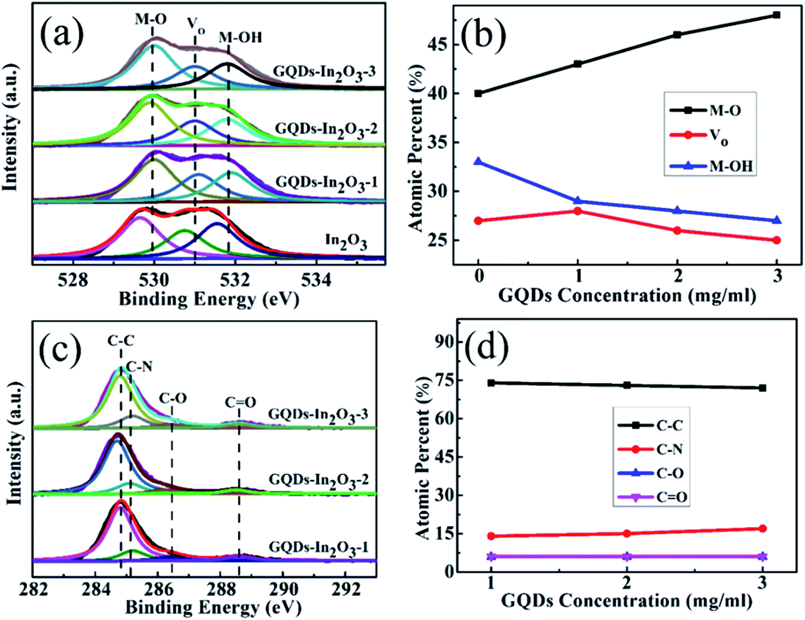 | ||
| Fig. 3 XPS spectra of (a) O 1s, (c) C 1s, and semiquantitative analyses of (b) oxygen-related, (d) carbon-related components in In2O3 thin films with different GQDs concentration. | ||
To confirm the possibility of solution-driven ZrOx dielectric thin film annealed at 600 °C as the dielectric layer, Al/ZrOx/Si MOS capacitor devices were fabricated and the dielectric properties and leakage current behavior were analyzed by an impedance analyzer. Fig. 4 displays the areal capacitance as a function of frequency in the range from 20 to 100 kHz. As shown in Fig. 4(a), the areal capacitance of ZrOx thin films annealed at 600 °C is measured to 301 nF cm−2 at 20 Hz and the calculated dielectric constant is 5.78. Compared to some reported values, the larger area capacitance at 20 Hz has been found, indicating the formation of ZrOx gate dielectric thin film with high quality. For field-effect devices, it is well-known that the dielectric with large area capacitance can induce more carriers at the interface between the semiconductor and the dielectric, thereby reducing the operating voltage. Meanwhile, a weaker frequency dispersion of capacitance for 600 °C-annealed ZrOx films has been observed, indicating the formation of denser metal-oxide bonding and much lower defect densities in ZrOx films such as hydroxyl group or oxygen vacancies in thin films. This will be of benefit to reduce the leakage current because the conduction paths in dielectrics are mainly caused by hydroxyl and grain boundaries. Fig. 4(b) shows the leakage current characteristics of MOS capacitors and a relatively low leakage current density (7.5 × 10⁻⁸ A cm−2 at 2 V), which is comparable to that of SiO2, has been found. The lower leakage current density comes from the gradually decomposition of residuals and reduction in the defect density. The dielectric layers possessing sufficiently low leakage current ensures that TFT devices have low OFF-state current and can operate at low voltage. AFM morphology of ZrOx dielectric films annealed at 600 °C is shown in the inset of Fig. 4(b) and RMS of 0.58 nm has been observed. Generally, the preferred smooth surface is conducive to the rapid transmission of carriers in narrow channel without suffering from electronic scattering and the formation of lower leakage current. Indeed, the smooth surface results from the reduction of the interface charge traps and dangling bonds, leading to the production of an excellent interface between the channel layer and the dielectric layer, which will contribute to high performance TFTs. Moreover, the achievement of dielectrics with small RMS will be of benefit to obtain high quality channel layer.46
 | ||
| Fig. 4 (a) Frequency-dependent areal capacitance of the ZrOx thin films annealed at 600 °C. (b) Leakage current density of the ZrOx thin films annealed at 600 °C. Inset shows the AFM image of ZrOx thin film annealed at 600 °C. | ||
The cross-sectional transmission electron microscopy (TEM) images of the complete devices, for example, with GQDs-In2O3-2 TFT shown in Fig. 5(a), confirm the expected thickness of each layer. The images also reveal excellent homogeneity of the films with uniform thickness. The scanning transmission electron microscopy (STEM) images obtained with elemental mappings (Fig. 5(b)–(f)) show high distribution uniformity of the elements with clear demarcation across the layers. All images show a clear boundary case, with no obvious interfaces spreading out or separating from each other, which helps to minimize the trapped charge. Based on STEM-ABF images shown in Fig. 5(h) and (i), it can be noted that many quantum dots are distributed in In2O3 films. To confirm the exact content of the QDs, the HRTEM images of the enlarged selected area marked with a red box, displayed in Fig. 5(k), shows that the materials have clear discernible lattice structures and the C–C bond is close to the ideal C–C bond for graphite.47 According to 2D fast Fourier transform (FFT) patterns (Fig. 5(i)), the esthetic hexagonal honeycomb structure with the bond lengths of 1.42 Å for C–C/CC has been observed,48 revealing that the GQDs have been successfully incorporated into In2O3 thin films.
 | ||
| Fig. 5 (a) (g) (j) Cross-sectional and zoomed-in area HRTEM images of the TFT with GQDs-In2O3/ZrOx/Si gate dielectrics. (b–f) Elemental mapping images across the cross section of the GQDs-In2O3-2 TFT. (b) Cross-sectional and zoomed-in area HRTEM images of the TFT. Inset, the FFT pattern. (h–i) STEM-ABF images of the GQDs-In2O3-2 TFT. (k) HRTEM images of the enlarged selected area marked with a red box. (l) The corresponding 2D FFT images. | ||
To investigate the feasibility of the GQDs-In2O3 thin films as the channel layers in TFTs, In2O3/ZrOx and GQDs-In2O3/ZrOx TFTs with bottom-gate and top-contact architectures were fabricated and shown in Fig. 6. The typical output characteristic curves of the In2O3/ZrOx and GQDs-In2O3-2/ZrOx TFTs at a VGS of 1.5 V are depicted in Fig. 6(a) and (b). It can be noted that these devices represent typical n-channel conduction behavior with clear pinch-off voltage and current saturation. Compared to GQDs-In2O3-2/ZrOx TFT, the output curves of In2O3/ZrOx TFT demonstrate the shifting trend towards right side (Fig. 6(a)). In addition, the higher gate voltage VGS is, the more the output curve right shifts, which can be attributed to the fact that the ohmic contact between Al electrodes and GQDs-In2O3-2 thin films is much better than that of In2O3 thin films. It can be observed that GQDs-In2O3-2 TFT represents a saturation current of 28.2 μA at 2.0 V, which is nearly 6 times larger than that of In2O3/ZrOx TFT. The obvious increase of on-current level of TFTs doped by GQDs can result from the relatively higher mobility of GQDs-In2O3 layers compared to In2O3 channel layers. The GQDs-embedded In2O3 TFTs demonstrate reasonably high on-current characteristics and we expect them to show stable unipolar switching characteristics. Fig. 6(c) shows the transfer characteristics of the In2O3 TFT in comparison with those of the three reference TFTs with different GQDs doping concentrations. The current between the source and the drain was measured at a static drain-source voltage of 2 V while the gate voltage changed from −1 V to 4 V.
 | ||
| Fig. 6 Output cure of (a) In2O3 TFT and (b) GQDs-In2O3-2 TFT. (c) Transfer characteristics of the In2O3 and GQDs-In2O3 TFTs. (d) Square-root of the transfer characteristics of the In2O3 and GQDs-In2O3 TFTs. The insets in (a) and (b) show the schematic illustration of the bottom-gate and top-contact In2O3-based TFTs. | ||
To investigate the evolution of the electrical properties of the In2O3 TFTs as a function of GQDs doping concentrations, key electrical parameters, including the field-effect mobility (μFE) and the threshold voltage (VTH), are calculated from the slope of IDS1/2 vs. VGS. All extracted TFTs performance parameters as a function of GQDs doping concentration are summarized in Table 1. It has been found that compared with pure In2O3 TFT, the μFE of GQDs-In2O3 TFTs increases obviously. It has been reported that the carrier concentration of oxide semiconductors can be increased obviously with C incorporation.49 The increase of the μFE of GQDs-In2O3 TFTs can be attributed to the higher electron mobility of graphene.50,51 However, excessive doping level of GQDs leads to the reduced μFE. As a result, it can be concluded that GQDs plays an important role in improving the mobility of TFTs device and the doping level should be controlled accurately. The extracted changes in VTH reveals that increasing the doping level of GQDs will lead to the increased positive VTH. This case can be attributed to the fact that the excess carrier concentration of In2O3 will be compensated by GQDs and remarkably shift VTH towards the positive values necessary for enhancement mode (E-mode) device characteristics has been observed. Based on Table 1, it can be also noted that compared to In2O3 TFTs, GQDs-In2O3 TFTs has a higher Ion/Ioff, which can be due to the increased Ion and the decreased Ioff. With increasing the GQDs doping level, the oxygen vacancy and free carrier concentration decrease. As a result, Ion/Ioff initially increases because of the reduced Ioff. However, further increasing the GQDs doping concentration leads to the degradation of the device performance, resulting from the increased trap states near the GQDs-In2O3/ZrOx TFTs interface.
| Samples | μFE (cm2 V−1 s−1) | Ion/Ioff | SS (V dec−1) | Dit (cm−2) | VTH (V) |
|---|---|---|---|---|---|
| In2O3 | 19.46 | 2.57 × 10⁶ | 0.11 | 1.60 × 10¹² | 0.92 |
| GQDs-In2O3-1 | 24.26 | 4.40 × 10⁶ | 0.10 | 1.11 × 10¹² | 0.98 |
| GQDs-In2O3-2 | 34.02 | 4.55 × 10⁷ | 0.08 | 5.84 × 10¹¹ | 1.22 |
| GQDs-In2O3-3 | 28.04 | 5.79 × 10⁶ | 0.12 | 2.03 × 10¹² | 0.81 |
Another electrical parameter, the subthreshold swing (SS), is calculated to be 0.11, 0.10, 0.08, and 0.12 V dec−1 for In2O3-based TFTs with different GQDs doping level. As we know, the SS value depends on the traps located in channel/dielectric interface and the lower SS can be expected to achieve a high operation speed and low power consumption. The small SS value of 80 mV dec−1 for GQDs-In2O3-2 sample is close to the theoretical limit (60 mV dec−1), which can originate from the large areal capacitance of the ZrOx dielectric layer and the electronic–clean interface between the channel layer and ZrOx.52 Based on the extracted SS, the Dit values of all In2O3-based TFTs with different GQDs doping content have been determined and listed in Table 1. Compared to In2O3-TFT, the reduction in Dit values for GQDs-In2O3 TFTs has been observed, indicating the reduction of the defect states and the formation of high quality GQDs-In2O3/ZrOx interface. With its large critical current density and high saturation speed, graphene has great potential for high-speed electronics.53 Appropriate GQDs doping may reduce the defect density at the interface between the channel layer and the gate dielectric layer, resulting in its small values of SS and Dit for GQDs-In2O3 TFT. The observed smallest Dit in GQDs-In2O3-2 is not only beneficial to carrier transport in the interface region, but also to the operation stability. However, for GQDs-In2O3-3 TFTs, the sharp increased Dit has been observed, which is in agreement with the evolution of the SS value. Excessive GQDs doping into In2O3 will introduce a large number of oxygen-containing functional groups, which will act as the trap states and trap mobile carriers, leading to the degraded the performance parameter of TFTs.
Based on above analyses, it can be concluded that compared with pure In2O3 TFT, solution-derived GQDs-In2O3-2 TFT exhibits impressive enhancement-mode device performance with a relatively smaller VTH of 1.22 V, an extraordinary on/off current ratio (>107), and a higher peak μFE of 32.02 cm2 (V−1 s−1). These excellent electrical properties are due to the structural flexibility of graphene.54 To our best knowledge, such a mobility is the highest compared with previous reports on In2O3-based TFTs via doping engineering route in recent years (indicated in Table 2). All these excellent device performances have guaranteed the potential application of GQDs-In2O3 TFTs in e-book and TFT-LCD. Particularly, all these parameters were obtained at a low operating voltage of 4 V, which is significant for low-power and green electronics.
| Samples | Mobility (cm2 V−1 s−1) | Ion/Ioff | SS (V dec−1) | Year | Ref. |
|---|---|---|---|---|---|
| Zn–In2O3 | 14.7 | 107 | 0.1 | 2015 | 55 |
| W–In2O3 | 15.3 | 107 | 0.07 | 2016 | 17 |
| Mg–In2O3 | 13.7 | 107 | 0.85 | 2017 | 26 |
| Y–In2O3 | 14.4 | 106 | 0.41 | 2019 | 20 |
| Ca– In2O3 | 15.1 | 107 | 0.08 | 2020 | 56 |
| C–In2O3 | 20.4 | 106 | 0.37 | 2021 | 57 |
| Zr–Al–In2O3 | 2.3 | 104 | 1.61 | 2021 | 58 |
| GQDs-In2O3 | 34.02 | 107 | 0.08 | This paper |
Since the TFT is the basic unit of integrated circuit, the operational stability of the TFT is a key electrical performance parameter, which determines their commercial applications such as the backplane of AMLCDs and AMOLEDs. The threshold voltage shift of TFTs will cause the decrease of display brightness and directly affect the display effect. To investigate the bias stability of the In2O3 and GQDs-In2O3-2 TFTs, positive and negative bias stress (PBS and NBS) measurements were carried out by applying a constant gate bias of 2.0 V while maintaining source and drain electrodes grounded. Fig. 7(a) and (b) display the transfer characteristics of the In2O3 and GQDs-In2O3-2 TFTs as a function of the stress time up to 3600 s. It can be seen that the TFT device with pure In2O3 channel layer suffers from positive threshold voltage shift (ΔVTH) of 0.69 V during PBS duration (Fig. 7(a)), indicating that more electrons are trapped near/at the dielectric and In2O3 interface. In contrast, the GQDs-In2O3-2 TFT demonstrates an improved PBS-induced stability with a smaller ΔVTH of 0.07 V up to 3600 s (Fig. 7(c)), indicating that appropriate GQDs doping suppressed the trapped charge in the film due to low interface states at the dielectric and channel interface, confirmed by previous Dit characterization. In addition, the observed parallel VTH shift and negligible change in the SS value indicates that no additional defect states are created at the channel/dielectric interface under bias stressing. Fig. 7(b) and (d) present the evolution of the transfer curves of the In2O3 and GQDs-In2O3-2 TFTs under NBS condition. The obvious left shift of the transfer curves in NBS has been observed, which may be caused by the release of electrons from oxygen defects in the active layer under the continuous gate bias stress. Compared to pure In2O3 TFT, the superior bias stability of the GQDs-In2O3-2 TFT device is preserved in cases of NBS testing. The negative VTH shifts after NBS application is 0.32 V for device with In2O3 channel layer (Fig. 7(b)). Conversely, the ΔVTH value for the GQDs-In2O3-2 TFT is reduced to ∼0.12 V (Fig. 7(d)). These results suggest that the charge trapping centers in the dielectric bulk region or ZrOx/In2O3 interfaces can be diminished by appropriate GQDs doing.
 | ||
| Fig. 7 Transfer curves under PBS test of (a) In2O3 TFT and (c) GQDs-In2O3-2 TFT. Transfer curves under NBS test of (b) In2O3 TFT and (d) GQDs-In2O3-2 TFT. Positive (e) and negative (f) threshold voltage shift as a function of stress time for In2O3 TFTs and GQDs-In2O3-2 TFTs. | ||
To confirm the dominant charge trapping mechanism causing the bias stress-induced the ΔVTH in TFTs, the relationship between the ΔVTH and the stress time has been summarized in Fig. 7(e) and (f). Results show that the time dependence of ΔVTH in the In2O3-based TFTs device follows a stretched exponential equation, originating from the charge being trapped at the dielectric/channel interface or getting injected into the gate dielectric. The time dependence of ΔVTH reflected by the stretched exponential model can be described as follows:

To further explain the mechanism of ΔVTH in the transfer curves, energy band diagrams of the GQDs-In2O3 TFTs device under PBS and NBS have been depicted in Fig. 8. When PBS measurement is performed in air atmosphere, excessive electrons will be accumulated in the GQDs-In2O3 channel. The surrounding oxygen molecules can capture electrons (acceptor, O2(g) + e− →O2(s)) from the conduction band and then adsorb on the TFT device. Therefore, the O2 adsorption in the channel layer can deplete the electron carriers and the buildup of negative space charge O2− easily will repel conduction electrons in the GQDs-In2O3 channel,60 leading to the positive VTH shift and the bending downwards of the energy band, as shown in Fig. 8(a) (Ef: Fermi energy level, Ec: conduction band, Ev: valence band, Ei: intermediate energy band). During the NBS process, the origination of NBS instability can also be attributed to the moisture absorption mechanism where this phenomenon can be expressed by the reaction equation H2O(g) + h+ → H2O+(s).61 Owing to the abundance of water molecular diffusing from the air ambient, this reaction will keep towards the right side and produce the mass of free electrons as demonstrated in Fig. 8(b), therefore the negative VTH shift has been detected. Under NBS, electrons will be depleted near the interface leading the energy band bending upwards.
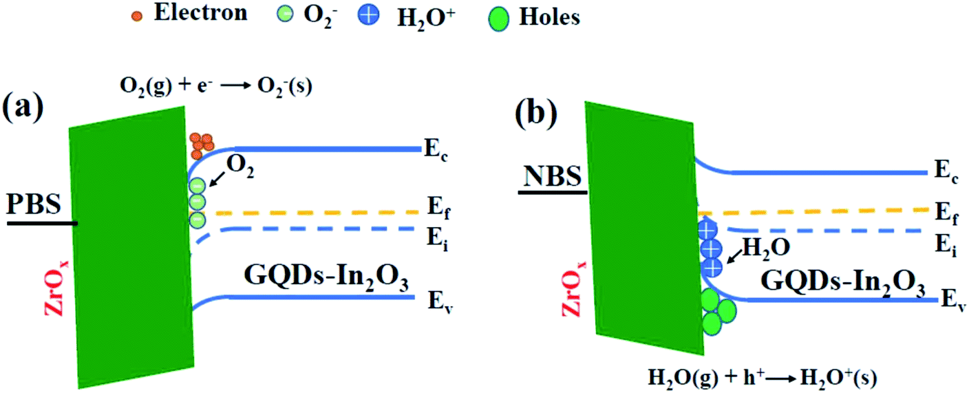 | ||
| Fig. 8 Bias instability mechanism for GQDs-In2O3 TFT under (a) PBS and (b) NBS. | ||
To investigate the compatibility of In2O3-based TFTs devices for circuit integration, their applications in inverter were further explored because the inverters are widely considered as the fundamental element which can be fabricated based on E-mode devices. In this work, the resistance-loaded inverters are constructed based on pure In2O3 and GQDS-In2O3-2 TFTs and a resistor of 10 MΩ and displayed in the inset of Fig. 9(c) and (d). As demonstrated in Fig. 9(a) and (b), the typical voltage transfer characteristic (VTC) curves at certain voltages (VDD) from 0.5 to 2.5 V with 0.5 V step have been found, indicating that a full swing of inverter characteristic is resulted with the input and output signals effectively rectified. The corresponding voltage gain (defined as −∂VOUT/∂VIN) is found to be 9.31 in maximum when VDD comes up to 2.5 V (Fig. 9(c)). When replacing In2O3 with GDQs-In2O3-2, the inverter characteristics can be substantially enhanced with a maximum voltage gain of 10.63 under the same VDD, as concluded in Fig. 9(e). Current extracted result is obviously superior to the reported inverters constructed by a single N-TFT, and even to some complementary inverters constructed by N-TFT and P-TFT.62,63 The high voltage gain of inverter benefits from high mobility, low off-state current, reliable stability and small subthreshold swing of TFT device. As reported, graphene plays an important role in the common source inverter due to its advantages such as het small transconductance, large drain conductance, and small back-gate capacitance.64 Another important performance parameter, the transition width, which defines the borders of the transition region, is also extracted and show in Fig. 9(f). It can be note that compared to the In2O3 TFT, the reduction in transition width has been observed after GQDS doping. In addition, the as-calculated maximum transition width of 0.40 V is lower than those previously reported resistor-loaded inverters based on In2O3 (2 V) and InGaZnO (3.8 V) transistors.65,66 The narrow transition width is expected to improve the responds characteristics of logic circuits.
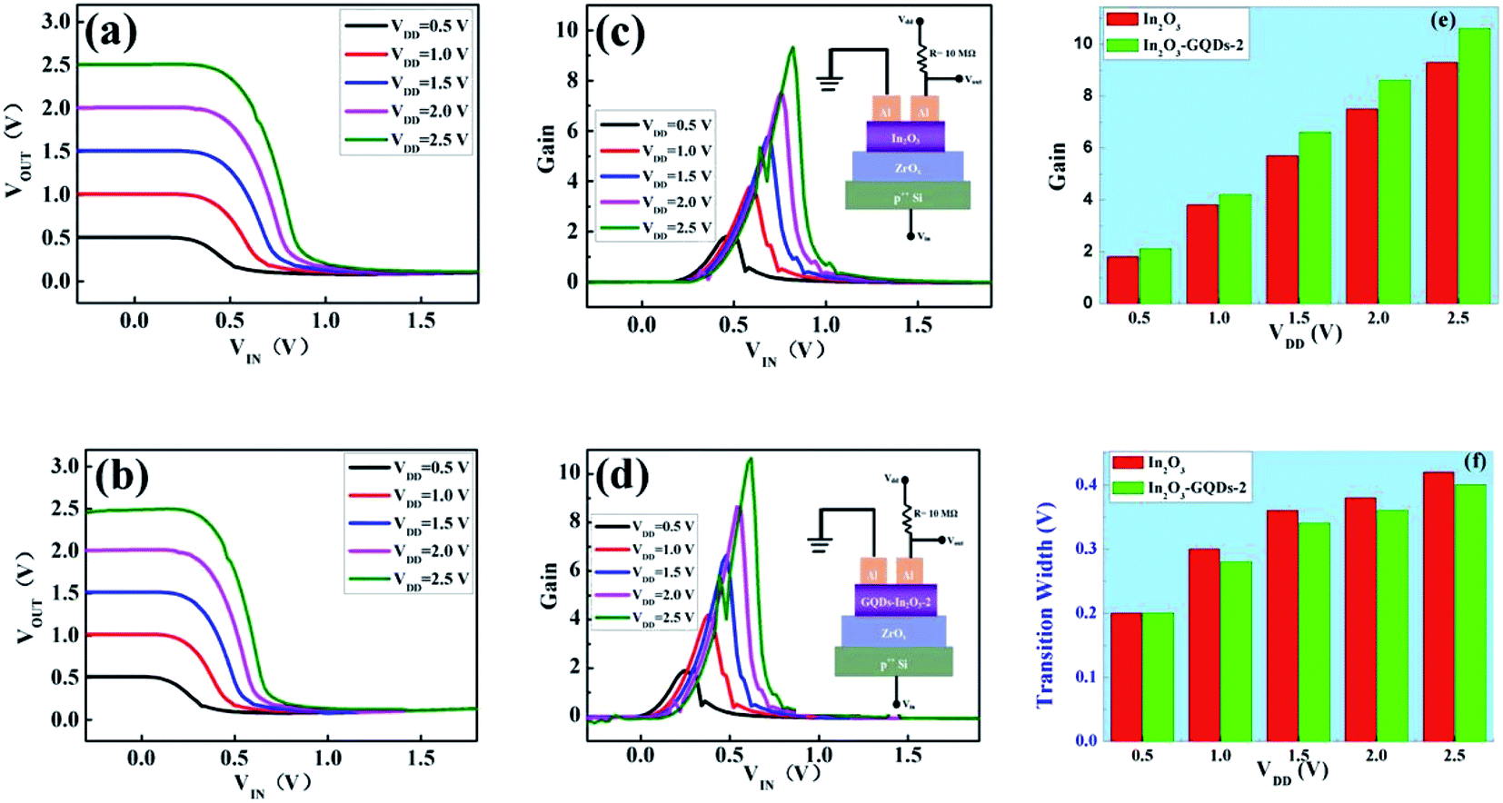 | ||
| Fig. 9 VTC curves of (a) In2O3 TFT and (b) GQDs-In2O3-2 TFT. Voltage gain of the inverter (c) In2O3 TFT and (d) GQDs-In2O3-2 TFT at different applied voltages. Insets in (c) and (d) are circuit schematic of the resistor-loaded inverters. Gain (e) and transition width (f) curves of In2O3 and GQDs-In2O3-2 TFTs as a function of VDD. | ||
Finally, low-frequency noise (LFN) measurements were carried out at room temperature for the pristine In2O3 and GQDs-In2O3-2 TFTs to investigate the reduction of the interface trap density and improvement in the stability of the In2O3 TFTs with GQDs doping with a fixed gate overdrive voltage (VGS − VTH) of 1.0 V together with VDS of 2.0 V, as shown in Fig. 10(a). The 1/f noise curves were obtained from the linear region of the curves. Based on the experimental results, it can be noted that it is in full accord with the classical 1/f noise theory.67 Observably, compared with the pure In2O3 TFT, the normalized drain current noise spectral density (SID/ID2) of GQDs-In2O3-2 TFT presents a decreasing trend, indicating that the average trap density and interface trap density for the In2O3-based TFT are reduced after GQDs doping. To further confirm the main source of LFN of In2O3-based TFTs, normalized SID/ID2 properties were estimated and analyzed, as demonstrated in Fig. 10(b). The experimental parameters for SID/ID2 measurement are as follows: VGS − VTH = (1–0.92) V, VDS = 2 V, and f = 20 Hz. The analysis of the results shows that the slopes of the curves for the pure In2O3 and GQDs-In2O3-2 are close to −1, indicating that the noise source mainly results from the fluctuations in mobility.68 The evolution law of the normalized drain current noise spectral density full conforms to previous electrical characterizations. As a result, it can be inferred that appropriate doping of GQDs is conductive to reducing trap density and improving the electrical properties and stability of In2O3 TFTs.
 | ||
| Fig. 10 (a) Typical LFN curves and (b) normalized SID/ID2 with different bias of the In2O3 and GQDs-In2O3-2 TFTs. | ||
Conclusion
In conclusion, this work reports a novel and effective solution-based method to prepare In2O3 TFTs with different GQDs doping amounts. Experimental results have found that GQDs-In2O3-2 TFT has exhibited excellent electrical performance, including a large μFE of 34.02 cm2 V−1 s−1, a high Ion/Ioff of 4.55 × 10⁷, a small SS of 0.08 V dec−1 and a small threshold voltage shift of 0.07 V and 0.12 V under PBS and NBS after 3600 s, respectively. On the basis of the GQDs-In2O3-2 TFT, inverter with a gain of 10.63 has been successfully constructed, demonstrating full swing characteristics. LFN measurements have concluded that the noise source can come from the fluctuations in mobility. The enhanced electrical performance and reliability of In2O3 TFTs can be ascribed to the appropriate incorporation of GQDs into the In2O3 channel layer, leading to the reduction of the interface trap density and oxygen vacancy states. All in all, the solution-derived GDQs-decorated oxide-based TFTs are promising for the development of transparent low-cost oxide thin film electronics.Conflicts of interest
There are no conflicts of interests or patent pending.Acknowledgements
The authors acknowledge the support from National Natural Science Foundation of China (11774001), Anhui Project (Z010118169).References
- J. H. Shen, Y. H. Zhu, X. L. Yang and C. Z. Li, Chem. Commun., 2012, 48, 3686 RSC.
- L. S. Li and X. Yan, J. Phys. Chem. Lett., 2010, 1, 2572 CrossRef CAS.
- D. Pan, J. Zhang, Z. Li and M. Wu, Adv. Mater., 2010, 22, 734 CrossRef CAS PubMed.
- L. L. Li, J. Ji, R. Fei, C. Z. Wang, Q. Lu, J. R. Zhang, L. P. Jiang and J. J. Zhu, Adv. Funct. Mater., 2012, 22, 2971 CrossRef CAS.
- Y. Shin, J. Lee, J. Yang, J. Park, K. Lee, S. Kim, Y. Park and H. Lee, Small, 2014, 10, 866 CrossRef CAS PubMed.
- Y. Wang, L. Zhang, R. P. Liang, J. M. Bai and J. D. Qiu, Anal. Chem., 2013, 85, 9148 CrossRef CAS PubMed.
- Z. S. Qian, X. Y. Shan, L. J. Chai, J. J. Ma, J. R. Chen and H. Feng, Biosens. Bioelectron., 2014, 60, 64 CrossRef CAS PubMed.
- W. W. Liu, Y. Q. Feng, X. B. Yan, J. T. Chen and Q. J. Xue, Adv. Funct. Mater., 2013, 23, 4111 CrossRef CAS.
- W. W. Liu, X. B. Yan, J. T. Chen, Y. Q. Feng and Q. J. Xue, Nanoscale, 2013, 5, 6053 RSC.
- P. O. Anikeeva, J. E. Halpert, M. G. Bawendi and V. Bulovic, Nano Lett., 2007, 7, 2196 CrossRef CAS PubMed.
- L. A. Ponomarenko, F. Schedin, M. I. Katsnelson, R. Yang, E. W. Hill, K. S. Novoselov and A. K. Geim, Science, 2008, 320, 356 CrossRef CAS.
- H. Tetsuka, R. Asahi, A. Nagoya, K. Okamoto, I. Tajima, R. Ohta and A. Okamoto, Adv. Mater., 2012, 24, 5333 CrossRef CAS PubMed.
- K. A. Ritter and J. W. Lyding, Nat. Mater., 2009, 8, 235 CrossRef CAS PubMed.
- B. Y. Su, S. Y. Chu, Y. D. Juang and S. Y. Liu, J. Alloys Compd., 2013, 580, 10 CrossRef CAS.
- S. Y. Han, G. S. Herman and C. H. Chang, J. Am. Chem. Soc., 2011, 133, 5166 CrossRef CAS PubMed.
- G. X. Jiang, A. Liu, G. X. Liu, C. D. Zhu, Y. Meng, B. Shin, E. Fortunato, R. Martins and F. K. Shan, Appl. Phys. Lett., 2016, 109, 183508 CrossRef.
- A. Liu, G. Liu, H. Zhu, B. Shin, E. Fortunato, R. Martins and F. K. Shan, J. Mater. Chem. C, 2016, 4, 4478 RSC.
- U. Ozgur, D. Hofstetter and H. Morkoc, Proc. IEEE, 2012, 98, 1255 Search PubMed.
- S. Parthiban and J. Y. Kwon, J. Mater. Res., 2014, 29, 1585 CrossRef CAS.
- J. Li, Y. H. Zhou, W. Q. Zhu, J. H. Zhang and Z. L. Zhang, Mater. Sci. Semicond. Process., 2019, 93, 201 CrossRef CAS.
- L. Lan, N. Xiong, P. Xiao, M. Li, H. Xu, R. Yao, S. Wen and J. Peng, Appl. Phys. Lett., 2013, 102, 242102 CrossRef.
- T. Hong, H. J. Jeong, H. M. Lee, S. H. Choi, J. H. Lim and J. S. Park, ACS Appl. Mater. Interfaces, 2021, 13, 28493 CrossRef CAS PubMed.
- S. Sugumaran, M. N. Bin Ahmad, M. F. Jamlos, C. S. Bellan, S. Chandran and M. Sivaraj, Opt. Mater., 2016, 54, 67 CrossRef CAS.
- K. Jang, J. Raja, Y. J. Lee, D. Kim and J. Yi, IEEE Electron Device Lett., 2013, 34, 1151 CAS.
- J. W. Hennek, M. G. Kim, M. G. Kanatzidis, A. Facchetti and T. J. Marks, J. Am. Chem. Soc., 2012, 134, 9593 CrossRef CAS PubMed.
- C. Y. Zhao, J. Li, D. Y. Zhong, C. X. Huang, J. H. Zhang, X. F. Li, X. Y. Jiang and Z. L. Zhang, IEEE Trans. Electron Devices, 2017, 64, 2216 CAS.
- H. H. Zhu, A. Liu, Y. Xu, F. K. Shan, A. Li, J. Wang, W. Yang, C. Barrow and J. Liu, Carbon, 2015, 88, 225 CrossRef CAS.
- H. H. Zhu, A. Liu, F. K. Shan, W. Yang, W. Zhang, D. Li and J. Liu, Carbon, 2016, 100, 201 CrossRef CAS.
- J. H. Park, Y. B. Yoo, K. H. Lee, W. S. Jang, J. Y. Oh, S. S. Chae, H. W. Lee, S. W. Han and H. K. Baik, ACS Appl. Mater. Interfaces, 2013, 5, 8067 CrossRef CAS PubMed.
- B. Yang, G. He, Y. Zhang, C. Zhang, Y. Xia, F. Alam and J. Cui, IEEE Trans. Electron Devices, 2019, 66, 3479 CAS.
- W. Wang, G. He, L. Wang, X. Xu and Y. Zhang, IEEE Trans. Electron Devices, 2021, 68, 4437 CAS.
- X. F. Xu, F. H. Gao, X. H. Bai, F. C. Liu, W. J. Kong and M. Li, Materials, 2017, 10, 1328 Search PubMed.
- C. Zhang, G. He, B. Yang, Y. F. Xia and Y. C. Zhang, IEEE Trans. Electron Devices, 2019, 66, 3854 Search PubMed.
- M. C. Nguyen, M. Jang, D. H. Lee, H. J. Bang, M. Lee, J. K. Jeong, H. Yang and R. Choi, Sci. Rep., 2016, 6, 25079 CrossRef CAS PubMed.
- Z. B. Zhuang, Q. Peng, J. F. Liu, X. Wang and Y. D. Li, Inorg. Chem., 2007, 46, 5179 CrossRef CAS PubMed.
- S. Stankovich, D. A. Dikin, R. D. Piner, K. A. Kohlhaas, A. Kleinhammes, Y. Jia, Y. Wu, S. T. Nguyen and R. S. Ruoff, Carbon, 2007, 45, 1558 CrossRef CAS.
- S. Hong, J. Park, K. Heejun, Y. G. Kim and H. J. Kim, J. Inf. Display, 2016, 17, 93 CrossRef CAS.
- J. M. Yuan, R. Zhao, Z. J. Wu, W. Li and X. G. Yang, Small, 2018, 14, 1703714 CrossRef PubMed.
- X. Wu, L. Ma, S. Sun, K. Jiang, L. Zhang, Y. Wang, H. Zeng and H. Lin, Nanoscale, 2018, 10, 1532 RSC.
- R. J. Hong, J. B. Huang, H. B. He, Z. X. Fan and J. D. Shao, Appl. Surf. Sci., 2005, 242, 346 CrossRef CAS.
- S. Neubeck, L. A. Ponomarenko, F. Freitag, A. J. M. Giesbers, U. Zeitler, S. V. Morozov, P. Blake, A. K. Geim and K. S. Novoselov, Small, 2010, 6, 1469 CrossRef CAS PubMed.
- Y. Jeong, K. Song, T. Jun, S. Jeong and J. Moon, Thin Solid Films, 2011, 519, 6164 CrossRef CAS.
- J. S. Lee, Y. J. Kwack and W. S. Choi, ACS Appl. Mater. Interfaces, 2013, 5, 11578 CrossRef CAS PubMed.
- G. Liu, A. Liu, H. H. Zhu, B. Shin, E. Fortunato, R. Martins, Y. Wang and F. K. Shan, Adv. Funct. Mater., 2015, 25, 2564 CrossRef CAS.
- Y. Li, Y. Hu, Y. Zhao, G. Shi, L. Deng, Y. Hou and L. Qu, Adv. Mater., 2011, 23, 776 CrossRef CAS.
- L. Zhu, G. He, J. Lv, E. Fortunato and R. Martins, RSC Adv., 2018, 8, 16788 RSC.
- S. Kim, S. W. Hwang, M. K. Kim, D. Y. Shin, D. H. Shin, C. O. Kim, S. B. Yang, J. H. Park, E. Hwang, S. H. Choi, G. Ko, S. Sim, C. Sone, H. J. Choi, S. Bae and B. H. Hong, ACS Nano, 2012, 6, 8203 CrossRef CAS PubMed.
- F. Joucken, F. Frising and R. Sporken, Carbon, 2015, 83, 48 CrossRef CAS.
- S. Akbar, S. K. Hasanain, M. Abbas, S. Ozcan, B. Ali and S. I. Shah, Solid State Commun., 2011, 151, 17 CrossRef CAS.
- K. S. Novoselov, A. K. Geim, S. V. Morozov, D. Jiang, Y. Zhang, S. V. Dubonos, I. V. Grigorieva and A. A. Firsov, Science, 2004, 306, 666 CrossRef CAS PubMed.
- J. Feng, H. Dong, B. Pang, Y. Chen, L. Yu and L. Dong, J. Mater. Chem. C, 2019, 7, 237 RSC.
- L. Zhu, G. He, W. D. Li, B. Yang, E. Fortunato and R. Martins, Adv. Electron. Mater., 2018, 4, 1800100 CrossRef.
- L. Liao, Y. C. Lin, M. Bao, R. Cheng, J. Bai, Y. Liu, Y. Qu, K. L. Wang, Y. Huang and X. Duan, Nature, 2010, 467, 305 CrossRef CAS PubMed.
- A. H. Castro Neto, F. Guinea, N. M. R. Peres, K. S. Novoselov and A. K. Geim, Rev. Mod. Phys., 2009, 81, 109 CrossRef CAS.
- F. Shan, A. Liu, G. X. Liu, Y. Meng, E. Fortunato and R. Martins, J. Disp. Technol., 2015, 11, 541 CAS.
- C. Zhang, G. He, W. H. Wang, Y. C. Zhang, Y. F. Xia and B. Yang, IEEE Trans. Electron Devices, 2020, 67, 4238 CAS.
- R. Kobayashi, T. Nabatame, T. Onaya, A. Ohi, N. Ikeda, T. Nagata, K. Tsukagoshi and A. Ogura, Jpn. J. Appl. Phys., 2021, 60, 030903 CrossRef CAS.
- D. Yao, X. Xiong, X. Fu, Z. Xu, H. Ning, D. Luo, H. Tang, H. Zheng, R. Yao and J. Peng, Surf. Interfaces, 2021, 27, 101459 CrossRef CAS.
- Y. C. Zhang, Y. J. Lin, G. He, B. H. Ge and W. J. Liu, ACS Appl. Electron. Mater., 2020, 2, 3728 CrossRef CAS.
- J. K. Jeong, H. W. Yang, J. H. Jeong, Y.-G. Mo and H. D. Kim, Appl. Phys. Lett., 2008, 93, 123508 CrossRef.
- P.-T. Liu, Y.-T. Chou and L.-F. Teng, Appl. Phys. Lett., 2009, 95, 233504 CrossRef.
- Y. J. Jeong, T. K. An, D.-J. Yun, L. H. Kim, S. Park, Y. Kim, S. Nam, K. H. Lee, S. H. Kim, J. Jang and C. E. Park, ACS Appl. Mater. Interfaces, 2016, 8, 5499 CrossRef CAS PubMed.
- S. K. Lee, S. M. H. Kabir, B. K. Sharma, B. J. Kim, J. H. Cho and J. H. Ahn, Nanotechnology, 2014, 25, 014002 CrossRef CAS PubMed.
- N. Harada, K. Yagi, S. Sato and N. Yokoyama, Appl. Phys. Lett., 2010, 96, 012102 CrossRef.
- L. Petti, H. Faber, N. Münzenrieder, G. Cantarella, P. A. Patsalas, G. Troter and T. D. Anthopoulos, Appl. Phys. Lett., 2015, 106, 092105 CrossRef.
- I. T. Cho, J. W. Lee, J. M. Park, W. S. Cheong, C. S. Hwang, J. S. Kwak, H. Cho, H. I. Kwon, H. Shin and B. G. Park, IEEE Electron Device Lett., 2012, 33, 1726 CAS.
- L. K. J. Vandamme and F. N. Hooge, IEEE Trans. Electron Devices, 2008, 55, 3070 Search PubMed.
- T. C. Fung, G. Baek and J. Kanicki, J. Appl. Phys., 2010, 108, 074518 CrossRef.
| This journal is © The Royal Society of Chemistry 2022 |