DOI:
10.1039/D2RA00849A
(Paper)
RSC Adv., 2022,
12, 16677-16683
Antiferromagnetic ordering in the TM-adsorbed AlN monolayer (TM = V and Cr)†
Received
9th February 2022
, Accepted 12th May 2022
First published on 6th June 2022
Abstract
In this work, the effects of transition metal (TM = V and Cr) adsorption on AlN monolayer electronic and magnetic properties are investigated using first-principles density functional theory (DFT) calculations. TMs prefer to be adsorbed on-top of a bridge position as indicated by the calculated adsorption energy. V adatoms induce half-metallicity, while Cr adatoms metallize the monolayer. The magnetic properties are produced mainly by the V and Cr adatoms with magnetic moments of 3.72 and 4.53 μB, respectively. Further investigation indicates that antiferromagnetic (AFM) ordering is energetically more favorable than ferromagnetic (FM) ordering. In both cases, the AFM state is stabilized upon increasing adatom coverage. The AlN monolayer becomes an AFM semiconductor with 0.5 ML of V adatom, and metallic nature is induced with 1.0 ML. Meanwhile, the degree of metallicity increases with increasing Cr adatoms. Results reported herein may provide a feasible new approach to functionalize AlN monolayers for spintronic applications.
1 Introduction
Following the promising reports of graphene and its derivatives,1–3 two-dimensional (2D) materials have drawn increasing attention because of their intriguing mechanical, physical and chemical properties.4,5 So far, a large variety of 2D materials have been explored for different applications including optoelectronics and photonics,6–8 spintronics,9,10 gas sensing,11,12 and energy production and storage.13,14 Among these, we highlight the family of nitrides with IIIA-group bases, as striking representatives.15–17 The planar hexagonal AlN monolayer was been predicted by Şahin et al.18 Results indicated the good dynamical stability and indirect gap insulator nature with an energy gap of 3.08(5.57) (eV) calculated at the LDA(GW0) theoretical level. Experimentally, epitaxial growth of ultrathin AlN nanosheets (sub-monolayer to monolayers) on the Ag(111) substrate was carried out by Tsipas et al.19 Experimental characterization provided evidence of the hexagonal structure and a smaller energy gap compared to that of the graphite-like AlN bulk compound. Later, the formation of the graphene-like AlN layer on Si(111) substrate was realized successfully by Mansurov et al.,20 which consists of the deposition of Al atoms under ammonia flux. A lattice parameter of 3.08 (Å) is obtained, which is in good agreement with theoretical ab initio calculations.
Using theoretical investigations on the AlN monolayer, researchers have devoted effort to modify its fundamental properties using different approaches. Almeida et al.21 have investigated the vacancies and antisite defects, and impurities in the AlN monolayer using first-principles calculations. A chemical bond length of 1.82 (Å) and indirect energy gap of 2.81 eV were obtained for the bare single layer. The results indicate that creating defects and doping may be efficient methods for tuning the electronic properties. Shi et al.22 demonstrated a significant magnetization of the AlN monolayer induced by transition metal (TM) doping due to the strong p–d hybridization. In addition, Mn- and Ni-doped systems may be suitable for spintronic applications exhibiting a half-metal character. Effects of thickness and external strain on the hexagonal AlN optoelectronic properties have been explored by Keçik et al.23 These results indicate important light absorption in the ultraviolet (UV) regime due to the large band gap, and this feature can be effectively tuned by varying the number of layers and applying external strain to extend the absorption to the visible (Vis) range. Using graphene-like AlN as an initial block, calculations by Yang et al.24 have revealed the direct gap and type-II band alignment of the AlN/BP heterobilayer. The fascinating UV-Vis absorption endows the material with promising applications in solar cell and photocatalytic water splitting. In previous work, we have explored the chemical functionalization of AlN monolayer using hydroxyl (–OH) group.25 An indirect–direct gap transition as well as energy gap reduction may be induced. Moreover, the pristine monolayer gap decreases when switching the external strain from compressive to tensile, and opposite behavior is obtained for the functionalized monolayer.
Previously, it has been proven that atom adsorption may be an efficient approach to make novel multifunctional 2D materials.26 In this regard, 3d TMs have been widely employed to induce magnetic properties due to their unpaired electrons. For example, the adsorption of 3d TMs on a MoS2 monolayer has been investigated by Wang et al.27 Their results indicate significant magnetization produced by Sc, V, Cr, Mn, Fe, Co and Cu adsorption, meanwhile the non-magnetic nature of MoS2 is preserved upon Ti, Ni, and Cu adsorption. Similarly, magnetism has been induced in InSe and g-C2N monolayers by TM adatoms for TMs from Sc to Co.28,29 In this work, the electronic and magnetic properties are probed to explore the effects of vanadium (V) and chromium (Cr) adsorption on the hexagonal AlN monolayer. TMs induce significant magnetization, breaking the spin symmetry of the bare monolayer. When more than one TM atom is adsorbed, they show antiferromagnetic alignment that is energetically more favorable than ferromagnetic ordering, similar to the effect observed in the TMs-adsorbed germanene monolayer.30 Results presented herein introduce new 2D antiferromagnetic semiconductor materials that may have spintronic applications as read-head devices and magnonic transport-based devices;31 while a small adatom concentration may lead to the formation of highly spin-polarized 2D materials to generate spin current.
2 Computational details
All calculations are based on the generalized gradient approximation with Perdew–Burke–Ernzerhof parameterisation (GGA-PBE)32 within the framework of density functional theory (DFT).33 The projector augmented wave (PAW) method, as implemented in the Vienna ab initio simulation package,34,35 is adopted to expand the electronic wave functions. The plane-wave expansion is carried out with an upper limit at 500 eV set as a kinetic energy cut-off. In each calculation, self-consistent iterations are set to converge to an energy criterion of 10−6 eV. To explore the effects of transition metal adsorption, a 2 × 2 × 1 supercell containing 4 Al atoms and 4 N atoms are modeled. In all systems, a vacuum layer larger than 15 Å is generated in the perpendicular direction, which helps to avoid inter-layer interactions. Structural relaxation is realized when the forces acting on the constituent atoms is below 0.01 eV Å−1. A Monkhorst–Pack k-mesh size36 of 10 × 10 × 1 is generated to integrate the Brillouin zone. In order to provide a reasonable treatment of the highly correlated TM-3d electrons, the GGA+U approach is employed. Herein, values of 3.0 eV and 0.6 eV are set for U and J parameters,37,38 respectively. It has been found that the weak van der Waals interactions have an insignificant effect on the electronic properties of the materials considered herein (see Fig. S1†).
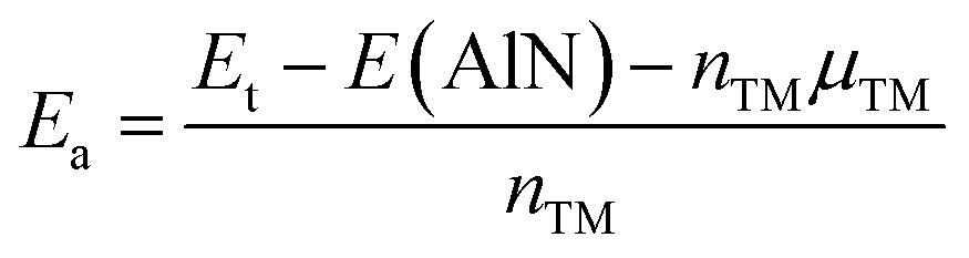
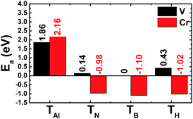
We have considered four high-symmetry adsorption sites: (1) on-top of the Al atom (TAl); (2) on-top of the N atom (TN); (3) on-top of the bridge position (TB); and (4) on-top of the hollow position (TH). In all cases, the energy adsorption Ea is calculated using the following equation:
| |
 | (1) |
where
Et and
E(AlN) refer to the energy of the adsorbed system and bare monolayer, respectively; while the number of adsorbed TM atoms and their chemical potential are denoted by
nTM and
μTM, respectively.
3 Results and discussion
3.1 Pristine AlN monolayer
Similar to the well known BN monolayer,39 the AlN monolayer may adopt a graphene-like hexagonal structure, in which Al and N atoms alternate to form a honeycomb arrangement as displayed in Fig. 1a. At equilibrium, the optimized geometry has a lattice parameter of 3.16 Å. In a planar structure characterized by a negligible buckling height and interatomic angle of 120°, the chemical bond length dAl–N takes value of 1.81 Å. These results are reasonable when compared with those of other VA-group nitride monolayers. Specifically, they are larger than those of BN and smaller than those of GaN and InN,18 according to the increase in atomic size: B → Al → Ga → In. In addition, good comparison with the results reported previously suggests their reliability.40 With one Al and one N atom in the primitive cell, six phonon modes (three acoustic and three optical) may appear in the phonon dispersion curves of the AlN monolayer. Results plotted in Fig. 1b indicate that the freestanding AlN monolayer is dynamically stable considering the absence of imaginary frequency in the spectrum.
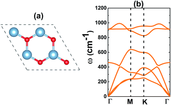 |
| | Fig. 1 (a) A 2 × 2 × 1 supercell (blue ball: Al atom; red ball: N atom) and (b) phonon dispersion curves of the AlN monolayer. | |
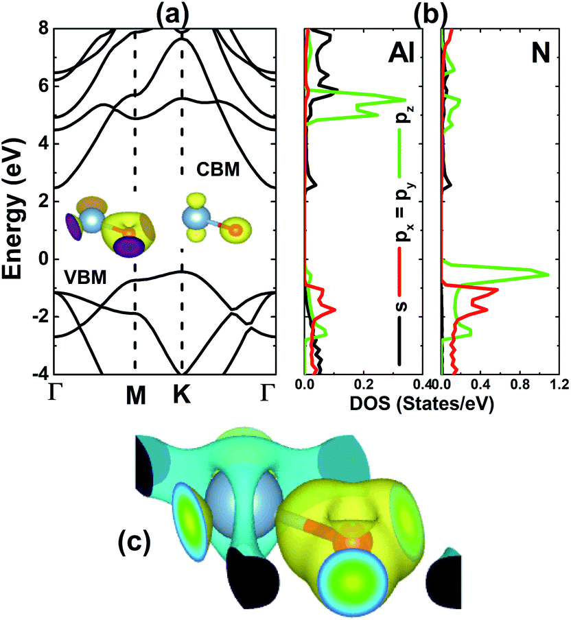
We have calculated the electronic band structure (BS) of the AlN monolayer along the Γ–M–K–Γ high symmetry direction, which is displayed in Fig. 2a. The BS profile confirms the semiconductor nature with a K–Γ indirect band gap of 2.91 eV, which compares well with previous calculations.18,25 The valence band maximum (VBM) energy curve is formed mainly by the N atom, meanwhile both constituents contribute to the formation of the conduction band minimum (CBM) energy curve. A deeper insight into BS formation can be analyzed by the projected density of states (PDOS) given in Fig. 2b. Note that in the energy range −4 to 8 eV, the valence band originates mainly from the O-p state, where pz states dominate in the higher energy region. The lower part of the conduction band is derived mainly from the outermost s orbital of both constituent atoms, meanwhile their pz state is the main contributor in the middle. The charge density difference Δρ, has been frequently employed to analyze the chemical bond of compounds. Herein, we have calculated this parameter using the following formula: Δρ = ρ(m) − ρ(Al) − ρ(N), where the right-hand-side terms refer to the charge density of the monolayer, Al atom and N atom, respectively. The results are illustrated in Fig. 2c. One can see a large charge accumulation at the N site generated by the charge transfer from the Al atom to N atom (from the less electronegative to more electronegative atom), suggesting the ionic character. However, it would be inaccurate to not mention the covalent character, which is suggested by the electronic hybridization (as shown in the PDOS spectra) and significant charge in the bridge positions. Therefore, one can conclude that a mix of ionic and covalent characters may hold the Al and N atoms together to form the monolayer.
 |
| | Fig. 2 (a) Electronic band structure, (b) projected density of states (DOS), and (c) charge density difference (yellow surface: charge accumulation; blue surface: charge depletion; iso-surface: 0.01) of the AlN monolayer. | |
3.2 V-adsorbed AlN monolayer
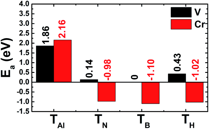
The results shown in Fig. 3 show that the V adatom prefers to be adsorbed on-top of the bridge position, considering the lowest adsorption energy with a value of 0.00 eV. From now on, only the electronic and magnetic properties of this stable system are studied, and it will be named V–AlN. V adsorption causes a low buckle ΔAl–N of 0.38 (Å) around the adsorption site. The interatomic distance from the V adatom to its nearest Al and N atoms is 2.59 and 2.24 (Å), respectively. Fig. 4a shows its spin-resolved band structure (BS). It can be noted that new electronic states appearing below the Fermi level in the spin-up channel, reduce the electronic band gap to 1.11 eV. Meanwhile, the others are induced in the lower part of the spin-down conduction band crossing the Fermi level. Consequently, the spin-down state exhibits metallic nature. The BS profile indicates the half-metallicity in the AlN monolayer induced by adsorbing the V atom. To gain more insight into the V adsorption effects, the projected density of states (PDOS) spectra are displayed in Fig. 4b to analyze the BS formation. In the considered energy range, the upper part of the valence band and lower part of the conduction band originate mainly from the host N-p, Al-s, and Al-p states. While the V atom contributes mainly around the Fermi level, which regulates the electronic properties of the system. The V-d orbital is split into the following states (in order of increasing energy): dyz–dxz, dxy–dx2 and dz2, which are induced mainly in the spin-up channel. Clearly, two two-fold degenerated states emerge in the valence band, and the last one takes place in the conduction band. Meanwhile, the Al-s state appears to be responsible for the spin-down metallic behavior considering its overlap with the Fermi level.
 |
| | Fig. 3 Calculated adsorption energy of V and Cr adatoms on the AlN monolayer (on-top of the Al atom (TAl); on-top of the N atom (TN); on-top of the bridge position (TB); and on-top of the hollow position (TH)). | |
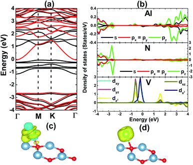 |
| | Fig. 4 (a) Spin-resolved band structure (black line: spin-up; red line: spin-down), (b) projected density of states, (c) charge density difference (yellow surface: charge accumulation; blue surface: charge depletion; iso-surface: 0.005), and (d) spin density (yellow surface: spin-up; iso-surface 0.02) of the V-adsorbed AlN monolayer. | |
The electronic distribution in the V–AlN system is further explored through charge density distribution (Δρ), which is calculated using the following function:
| | |
Δρ = ρ(V–AlN) − ρ(AlN) − ρ(V)
| (2) |
where
ρ(V–AlN),
ρ(AlN), and
ρ(V) denote the charge density of the V-adsorbed monolayer, bare monolayer, and isolated V atom, respectively. Results are illustrated in
Fig. 4c. The most remarkable charge distribution modification is noted mainly around the V adatom, where both charge accumulation and loss processes take place. Moreover, an increase of charge density occurs in the V–Al bridge position, and a smaller accumulation is also noted in the region between the V and N atoms. These features suggest significant interactions between the V adatom and host atoms. Mostly, a partial charge transfer process may occur from the V adatom (spin-up d
z2 state) towards the Al atom (spin-down s state), which is consistent with the PDOS spectra analyzed above. The BS and PDOS spin-asymmetry profile may suggest important magnetization of the AlN monolayer upon V adsorption, which can be analyzed
via the spin density distribution illustrated in
Fig. 4d. Note that the magnetic properties are produced mainly by the V adatom, which is the main effect responsible for breaking the AlN monolayer spin-symmetry. This result is supported by a magnetic moment as large as 3.72 (
μB), meanwhile the Al and N atoms exhibit quite small values between 0.01 and 0.03 (
μB). The magnetic half-metallicity feature suggests that the AlN monolayer may be functionalized for spintronic applications upon adsorbing single V atoms.
Further study of the effects of V atom adsorption is carried out with different monolayer coverage (ML); specifically, different coverage of 0.5 ML and 1.0 ML (two and four V adatoms on a 2 × 2 × 1 supercell, respectively). Possible ferromagnetic (FM) and antiferromagnetic (AFM) spin alignments are shown in Fig. 5. As a first step, the stable magnetic state is determined by the energy difference (ΔE) as follows:
Herein, the total energy of the FM and AFM states are denoted by
EFM and
EAFM, respectively.
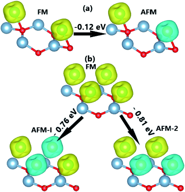
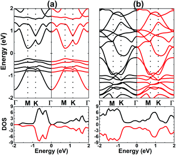
Fig. 5 indicates that the AFM state is stable at both coverages, where the type-II AFM state is energetically more favorable in comparison with the type-I one for the case of 1.0 ML. The more V adatoms adsorbed, the more stable the AFM state. Applying
eqn (1), we obtained adsorption energies of −0.61 and −1.49 eV per atom, for 0.5 ML and 1.0 ML, respectively. Results indicate that the V-adsorbed AlN monolayer becomes more stable upon increasing adatom concentration. The AFM state is also confirmed considering a larger supercell size of 4 × 4 × 1, where the energy for the magnetic state transition is −40 meV (see Fig. S2
†). Through
ab initio molecular dynamics (AIMD) calculations, we observed no structural destruction suggesting good thermal stability for all V-adsorbed systems at the different coverages (see Fig. S3a–c
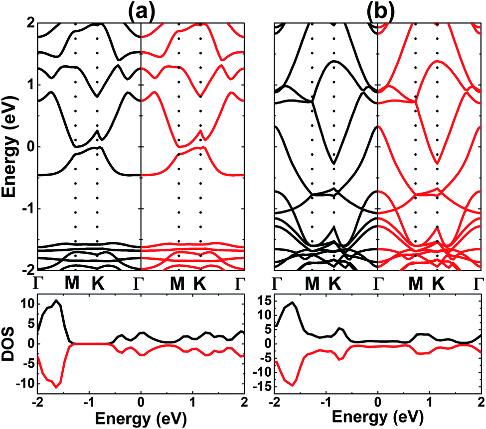
†). The spin-resolved BS and DOS of stable systems are given in
Fig. 6, which shows the complete spin-symmetry. A 0.5 ML adatom coverage decreases the energy gap to 0.46 eV, which corresponds to a reduction of the order of 84.19% as compared to that of the bare monolayer. Meanwhile, the full coverage of 1.0 ML leads to the formation of a antiferromagnetic metallic 2D material since the lower part of the conduction band crosses the Fermi level, which may be caused by large quantities of charge transferred from the adatoms to Al atoms. According to our calculations, V atoms have magnetic moments of ±3.40 and ±3.20 (
μB) in the V-adsorbed AlN monolayer at 0.5 ML and 1.0 ML, respectively.
 |
| | Fig. 5 Energy of the magnetic state transitions of V-adsorbed AlN monolayer with a coverage of (a) 0.5 ML and (b) 1.0 ML (yellow surface: spin-up; blue surface: spin-down; iso-surface: 0.02). | |
 |
| | Fig. 6 Spin-resolved band structure and density of states (black line: spin-up; red line: spin-down) of V-adsorbed AlN monolayer with coverage of (a) 0.5 ML and (b) 1.0 ML. | |
3.3 Cr-adsorbed AlN monolayer
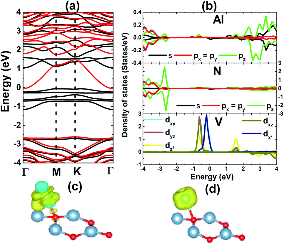
Now the adsorption of Cr atoms on the AlN monolayer is explored. Similar to the previous case, Cr may be adsorbed on-top, the TB position, with an adsorption energy of −1.10 (eV) (see Fig. 1), suggesting chemisorption. Once adsorbed on the AlN monolayer, the Cr adatom induces a wrinkle ΔAl–N of 0.49 (Å) around the adsorption site. Besides, the bond lengths dCr–Al and dCr–N, take values of 2.48 and 2.03 (Å), respectively. Note that these values are smaller than their counterparts in the V-adsorbed system. In combination with the calculated adsorption energy, one can conclude that Cr adsorption on the AlN monolayer is stronger than V adsorption. The BS profile displayed in Fig. 7a indicate the metallization of the AlN monolayer upon adsorbing a single Cr atom. Specifically, flat energy branches cross the Fermi level in both spin channels, giving rise to the metallic nature. Analyzing the PDOS spectra in Fig. 7b, we observe the significant presence of spin-up Cr-d states around the Fermi level. This feature is dissimilar to the case of V adsorption, which may be due to the large number of valence electrons of the Cr atom (3d4) in comparison with the V atom (3d3), such that the Cr-d states shift to lower energies to generate the spin-up metallic behavior with dyz, dxz, and dz2 states the main contributors. Meanwhile, the spin-down metallicity is caused mainly by the Al-s state, suggesting a charge transfer from the adatom to Al atom. The charge density difference illustrated in Fig. 7c supports this feature, where significant charge accumulation is noted in the bridge Cr–Al position due to the electronic interactions. Magnetism in the Cr–AlN system is generated mainly by the adatom as indicated by the spin density illustration in Fig. 7d, which has a magnetic moment of 4.53 (μB). In contrast, host atoms exhibit negligible magnetization with small magnetic moments varying between −0.01 and 0.03 (μB).
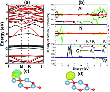 |
| | Fig. 7 (a) Spin-resolved band structure (black line: spin-up; red line: spin-down), (b) projected density of states, (c) charge density difference (yellow surface: charge accumulation; blue surface: charge depletion; iso-surface: 0.005), and (d) spin density (yellow surface: spin-up; iso-surface 0.02) of the Cr-adsorbed AlN monolayer. | |
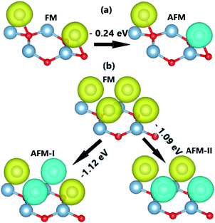
Upon increasing the adatom concentration, the AFM state may be energetically more stable than the FM state (see Fig. 8). Specifically, AFM ordering exhibits an energy of 0.24 eV, smaller than the FM ordering with a coverage of 0.5 ML. The difference is larger in the case of 1.0 ML (between 1.09 and 1.12 eV), suggesting stabilization of the AFM state with increasing adatom concentration. In this case, type-I AFM ordering is the most stable with an energy 0.03 eV smaller than type-II. A smaller adatom concentration is also considered in a 4 × 4 × 1 supercell, where the AFM state is energetically favorable with an energy 70 meV smaller than the FM state (see Fig. S2†). When more Cr atoms are adsorbed on the AlN monolayer, the system may exhibit higher stability since the adsorption energy takes a more negative value for 1.0 ML (−2.63 eV per atom) than 0.5 ML (−1.80 eV atom). In addition, AIMD calculations show good thermal stability at different coverages of Cr adatoms since constituent atoms vibrate around their sites without further bond breaking (see Fig. S3d–f†). Our simulations yield magnetic moments of ±4.38 and ±4.34 (μB) in the Cr-adsorbed AlN monolayer with adatom coverage of 0.5 ML and 1.0 ML. respectively. In the AFM state with equal absolute magnetic moments (a total value of 0 μB), the BS and DOS show a complete spin-symmetry as displayed in Fig. 9. Note that both systems are electrically metallic, and the degree of metallicity increases when more Cr atoms are adsorbed, considering the valence band maximum shifts to higher energy and opposite behavior is noted for the conduction band minimum. These features may be due to an increase of Cr-3d valence electrons, leading to higher occupancy of the outermost orbitals.
 |
| | Fig. 8 Energy of the magnetic state transitions of the Cr-adsorbed AlN monolayer with coverage of (a) 0.5 ML and (b) 1.0 ML (yellow surface: spin-up; blue surface: spin-down; iso-surface: 0.02). | |
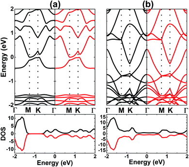 |
| | Fig. 9 Spin-resolved band structure and density of states (black line: spin-up; red line: spin-down) of V-adsorbed AlN monolayer with coverage of (a) 0.5 ML and (b) 1.0 ML. | |
4 Conclusions
In summary, the effect of V or Cr adsorption on AlN monolayer electronic and magnetic properties, has been systematically investigated using first-principles calculations. The pristine monolayer exhibits good dynamical stability and has an indirect band gap of 2.91 eV, whose band structure is formed mainly by the Al-s, Al-p, and N-s states. Significant ionic character is also confirmed by the charge density difference. Adsorption on-top of the bridge position is demonstrated to be the favorable site at which adatoms are chemically adsorbed. Electronic and magnetic properties of the adsorbed systems are regulated mainly by the TM-d orbital, which emerges in the AlN monolayer forbidden energy region. Half-metallicity, generated by a semiconductor spin-up state and a metallic spin-down state, is induced by adsorbing a single V atom. In contrast, metallization takes place once a single Cr atom is adsorbed. The dissimilarity can be attributed to the larger number of valence electrons in a Cr atom compared with a V atom. Upon increasing the adatom coverage, the systems become more stable and adatoms are adsorbed more strongly. In addition, the antiferromagnetic state is stabilized at high adatom concentrations. A V coverage of 0.5 ML leads to the formation of an AFM semiconductor material with an energy gap of 0.46 eV, meanwhile a higher coverage of 1.0 ML induces the metallization. Under different Cr coverage, the AlN monolayer is metallized and the metallicity becomes stronger at high coverage. In all cases, the magnetic properties are produced mainly by transition metals with a strong spin-asymmetric d orbital. Results pave the way to inducing new features in the AlN monolayer to make it suitable for spintronic applications.
Conflicts of interest
The authors declare that they have no known competing financial interests or personal relationships that could have appeared to influence the work reported in this paper.
Acknowledgements
Calculations were performed in the high-performance computing cluster (HPCC) of Thu Dau Mot University (TDMU).
Notes and references
- K. S. Novoselov, A. K. Geim, S. V. Morozov, D.-e. Jiang, Y. Zhang, S. V. Dubonos, I. V. Grigorieva and A. A. Firsov, Science, 2004, 306, 666–669 CrossRef CAS PubMed.
- X. J. Lee, B. Y. Z. Hiew, K. C. Lai, L. Y. Lee, S. Gan, S. Thangalazhy-Gopakumar and S. Rigby, J. Taiwan Inst. Chem. Eng., 2019, 98, 163–180 CrossRef CAS.
- M. Tahriri, M. Del Monico, A. Moghanian, M. T. Yaraki, R. Torres, A. Yadegari and L. Tayebi, Mater. Sci. Eng., C, 2019, 102, 171–185 CrossRef CAS PubMed.
- G. Zhang and Y.-W. Zhang, Chin. Phys. B, 2017, 26, 034401 CrossRef.
- P. Miró, M. Audiffred and T. Heine, Chem. Soc. Rev., 2014, 43, 6537–6554 RSC.
- J. S. Ponraj, Z.-Q. Xu, S. C. Dhanabalan, H. Mu, Y. Wang, J. Yuan, P. Li, S. Thakur, M. Ashrafi and K. Mccoubrey, et al., Nanotechnology, 2016, 27, 462001 CrossRef PubMed.
- A. Bablich, S. Kataria and M. C. Lemme, Electronics, 2016, 5, 13 CrossRef.
- F. Xia, H. Wang, D. Xiao, M. Dubey and A. Ramasubramaniam, Nat. Photonics, 2014, 8, 899–907 CrossRef CAS.
- Y. Liu, C. Zeng, J. Zhong, J. Ding, Z. M. Wang and Z. Liu, Nano-Micro Lett., 2020, 12, 1–26 CrossRef PubMed.
- N. Sethulakshmi, A. Mishra, P. M. Ajayan, Y. Kawazoe, A. K. Roy, A. K. Singh and C. S. Tiwary, Mater. Today, 2019, 27, 107–122 CrossRef CAS.
- S. S. Varghese, S. H. Varghese, S. Swaminathan, K. K. Singh and V. Mittal, Electronics, 2015, 4, 651–687 CrossRef CAS.
- E. Lee, Y. S. Yoon and D.-J. Kim, ACS Sens., 2018, 3, 2045–2060 CrossRef CAS PubMed.
- H. Tao, Q. Fan, T. Ma, S. Liu, H. Gysling, J. Texter, F. Guo and Z. Sun, Prog. Mater. Sci., 2020, 111, 100637 CrossRef CAS.
- Y. Xue, Q. Zhang, W. Wang, H. Cao, Q. Yang and L. Fu, Adv. Energy Mater., 2017, 7, 1602684 CrossRef.
- K. K. Kim, A. Hsu, X. Jia, S. M. Kim, Y. Shi, M. Hofmann, D. Nezich, J. F. Rodriguez-Nieva, M. Dresselhaus and T. Palacios, et al., Nano Lett., 2012, 12, 161–166 CrossRef PubMed.
- D. Hoat, M. Naseri, T. V. Vu, H. L. Luong, N. N. Hieu, R. Ponce-Pérez, J. Rivas-Silva and G. H. Cocoletzi, Superlattices Microstruct., 2019, 136, 106270 CrossRef CAS.
- B. Meng, W.-Z. Xiao, L.-L. Wang, L. Yue, S. Zhang and H.-y. Zhang, RSC Adv., 2015, 5, 82357–82362 RSC.
- H. Şahin, S. Cahangirov, M. Topsakal, E. Bekaroglu, E. Akturk, R. T. Senger and S. Ciraci, Phys. Rev. B: Condens. Matter Mater. Phys., 2009, 80, 155453 CrossRef.
- P. Tsipas, S. Kassavetis, D. Tsoutsou, E. Xenogiannopoulou, E. Golias, S. Giamini, C. Grazianetti, D. Chiappe, A. Molle and M. Fanciulli, et al., Appl. Phys. Lett., 2013, 103, 251605 CrossRef.
- V. Mansurov, T. Malin, Y. Galitsyn and K. Zhuravlev, J. Cryst. Growth, 2015, 428, 93–97 CrossRef CAS.
- E. de Almeida, F. de Brito Mota, C. De Castilho, A. Kakanakova-Georgieva and G. K. Gueorguiev, Eur. Phys. J. B, 2012, 85, 1–9 CrossRef.
- C. Shi, H. Qin, Y. Zhang, J. Hu and L. Ju, J. Appl. Phys., 2014, 115, 053907 CrossRef.
- D. Keçik, C. Bacaksiz, R. T. Senger and E. Durgun, Phys. Rev. B: Condens. Matter Mater. Phys., 2015, 92, 165408 CrossRef.
- Q. Yang, C.-J. Tan, R.-S. Meng, J.-K. Jiang, Q.-H. Liang, X. Sun, D.-G. Yang and X.-P. Chen, IEEE Electron Device Lett., 2016, 38, 145–148 CAS.
- D. Hoat, M. Naseri, N. T. Binh, J. Rivas-Silva, T. V. Vu and G. H. Cocoletzi, Phys. Lett. A, 2020, 384, 126444 CrossRef CAS.
- Y. You, H. Hu and J.-H. Choi, Phys. Chem. Chem. Phys., 2021, 23, 9814–9821 RSC.
- Y. Wang, B. Wang, R. Huang, B. Gao, F. Kong and Q. Zhang, Phys. E, 2014, 63, 276–282 CrossRef CAS.
- W. Ju, T. Li, Q. Zhou, H. Li, X. Li and D. Ma, Comput. Mater. Sci., 2018, 150, 33–41 CrossRef CAS.
- Z. Zheng, X. Wang and W. Mi, Carbon, 2016, 109, 764–770 CrossRef CAS.
- T. P. Kaloni, J. Phys. Chem. C, 2014, 118, 25200–25208 CrossRef CAS.
- D. Wu, Z. Zhuo, H. Lv, K. Zhang, Y. Ji, P. Wang, X. Luo, X. Wu and J. Yang, ACS Appl. Nano Mater., 2021, 4, 10877–10885 CrossRef CAS.
- J. P. Perdew, K. Burke and M. Ernzerhof, Phys. Rev. Lett., 1996, 77, 3865 CrossRef CAS PubMed.
- W. Kohn and L. J. Sham, Phys. Rev., 1965, 140, A1133 CrossRef.
- G. Kresse and J. Furthmüller, Comput. Mater. Sci., 1996, 6, 15–50 CrossRef CAS.
- G. Kresse and J. Furthmüller, Phys. Rev. B: Condens. Matter Mater. Phys., 1996, 54, 11169 CrossRef CAS PubMed.
- H. J. Monkhorst and J. D. Pack, Phys. Rev. B: Solid State, 1976, 13, 5188 CrossRef.
- M. Cococcioni and S. De Gironcoli, Phys. Rev. B: Condens. Matter Mater. Phys., 2005, 71, 035105 CrossRef.
- J.-J. Xian, C. Wang, J.-H. Nie, R. Li, M. Han, J. Lin, W.-H. Zhang, Z.-Y. Liu, Z.-M. Zhang and M.-P. Miao, et al., Nat. Commun., 2022, 13, 1–9 Search PubMed.
- K. Ba, W. Jiang, J. Cheng, J. Bao, N. Xuan, Y. Sun, B. Liu, A. Xie, S. Wu and Z. Sun, Sci. Rep., 2017, 7, 1–8 CrossRef PubMed.
- Y. Bai, K. Deng and E. Kan, RSC Adv., 2015, 5, 18352–18358 RSC.
|
| This journal is © The Royal Society of Chemistry 2022 |
Click here to see how this site uses Cookies. View our privacy policy here. 
 Open Access Article
 This Open Access Article is licensed under a Creative Commons Attribution-Non Commercial 3.0 Unported Licence
 *de
*de