DOI:
10.1039/D2RA00775D
(Paper)
RSC Adv., 2022,
12, 13749-13755
Janus transition metal dichalcogenides in combination with MoS2 for high-efficiency photovoltaic applications: a DFT study†
Received
5th February 2022
, Accepted 1st May 2022
First published on 6th May 2022
Abstract
Exotic features of two-dimensional materials have been demonstrated, making them particularly appealing for both photocatalytic and photovoltaic applications. van der Waals corrected density functional theory calculations were performed on AAII-Se MoSSe, AAII-Te MoSTe, and AAII-Se WSSe heterostructures in this study. Our findings reveal that the heterostructures have high stability due to the tiny lattice mismatch and binding energy, which is extremely favorable for epitaxial growth of these heterostructures. According to the electronic band gap calculation, AAII-Se MoSSe and AAII-Se WSSe are semiconducting materials, while AAII-Te MoSTe has metallic properties. Interestingly, all three heterostructures have type II band gap alignment, which is advantageous for photovoltaic and photocatalytic applications. Furthermore, it was discovered that AAII-Se MoSSe and AAII-Se WSSe heterostructures exhibit high power conversion efficiency of up to 12.15% and 9.37%, respectively. Based on these intriguing features, the two heterostructures are excellent prospects for photovoltaic applications. The heterostructures have no appropriate band edge sites for overall water splitting at pH = 0, but they are good for the oxygen evolution process. It is feasible to alter the position of the band edges using strain resulting in improved overall water splitting by the heterostructures.
Introduction
The discovery of 2D materials has accelerated1,2 since the discovery of graphene in 2004,3 including that of molybdenum disulphide (MoS2)4,5 graphitic carbon nitride (g-C3N4),6,7 phosphorene,8,9 and MXenes.10–12 The piqued interest of many researchers is because of their exceptional electronic and mechanical properties as well as possible application in nanodevices. In addition, a number of derivatives of 2D materials are emerging, such as spliced 3D compounds, Janus 2D materials and 2D van der Waals heterojunctions.13–17 2D van der Waals (vdW) heterojunctions are gaining significant attention because it combines the advantages of different from monolayers. These 2D heterostructures combines two or more different layered materials, which could result in novel properties and potential applications.18,19 The relative weak interlayer coupling of heterostructures allows for most of the intrinsic properties from the individual monolayers to remain intact.20 Thus, the opportunities to combine the intrinsic different properties of various monolayers is an underlying advantage of heterostructures.20 Also, 2D vdW heterostructure could overcome the shortcomings of single materials, such as low quantum efficiency, high charge recombination, and serious chemical back-reactions.21,22
The world's finite energy supplies of non-renewable and need to decarbonize to meet the growing need for energy calls for the need to rapidly develop renewable energy. As a result, photocatalytic water splitting, and solar cell technology have been seen as two suitable approaches to providing clean energy. Several studies have been carried out, which focused on finding an efficient photocatalyst23–27 and solar cell28–30 materials, such as the development of MoS2 monolayer as a potential photocatalyst for water splitting31–33 and solar cell34 applications. The photogenerated electron–hole pairs in MoS2, on the other hand, remain in the same spatial locations, resulting in a high rate of recombination. Photogenerated electron–hole pairs in the MoS2 monolayer, remain in the same spatial locations resulting in a high rate of recombination. vdW heterostructures can overcome this issue while also providing improved overall characteristics. There are three types of band alignment for semiconductor heterojunction, including straddling gap (type I), staggered gap (type II) and broken gap (type III).35 Because the valence-band maximum (VBM) and conduction-band minimum (CBM) reside in distinct layers, type-II (staggered)36 heterostructures appear promise for achieving efficient charge carrier separation. As a result, when photogenerated electron–hole couples break at the interface, the electrons are moved to one layer and the holes are sent to another. This property makes type-II heterostructures ideal for use in photovoltaic and photocatalytic devices. Wang, S. et al.37 investigated photocatalytic devices based on MoS2/ZnO van der Waals heterostructure and Bernardi et al.38 investigated photovoltaic devices based on the MoS2/WS2 bilayer. Both studies discovered that the heterostructures exhibit type-II band edge alignment. From their investigations, the band edge positions satisfy the energy levels required for the water splitting reaction in the photocatalytic application, and as a photovoltaic device, the power-conversion efficiency of up to 1% and a far higher power density than existing ultrathin solar cells was observed. The findings showed that creating hetero-structured materials based on MoS2 have potential application for photocatalytic water splitting and photovoltaic.
Recently Janus 2D materials particularly Janus transition metal dichalcogenides (TMD) material, are gaining increasing attention due to their distinct properties, which are different from the traditional 2D materials.31 Unlike typical TMDs, Janus TMD (JTMD) monolayers lack both in-plane and out-of-plane symmetries, giving them an extra degree of freedom to regulate their properties.32,39,40 Using chemical vapor deposition technique, a JTMD material (i.e., MoSSe) was recently produced experimentally by selective selenization of the top atomic layer in a single-layer MoS2.41,42 JTMD's fascinating features imply that they are crucial 2D materials. Furthermore, unlike traditional vdW heterostructures, the intrinsic interlayer polarization from Janus material will couple with the interlayer built-in polarization field, providing an additional degree of freedom to modulate the physical/chemical properties of the heterostructure, resulting in novel features and potential applications.20
We used ab initio calculations to determine the structural and electrical properties of the MoS2/JTMD (JTMD = MoSSe, MoSTe, MoSeTe, WSSe, and WSeTe) bilayer in this study. The calculated binding energies of the bilayer system indicates that configurations AAII-Se MoSSe, AAII-Te MoSTe and AAII-Se WSSe is stable. The calculated electronic band gap for the two heterostructure is semiconducting and one shows metallic property. The AAII-Se MoSSe, AAII-Te MoSTe and AAII-Se WSSe vdW heterostructures forms a typical type-II band alignment, which lead to effective separation of electron–hole pairs. Moreover, the AAII-Se MoSSe and AAII-Se WSSe vdW heterostructure also exhibits very good power conversion efficiency with a value of (7.289–12.15%) and (5.62–9.37%) respectively suggesting that they are a good candidate for photovoltaic applications. The heterostructures might be a suitable material for photocatalytic water splitting if strain is applied on them.
Computational method
Density functional theory (DFT)43 with the projected augmented wave (PAW) and generalized gradient approximation (GGA)44 with the PBE variant as implemented in the Quantum ESPRESSO and CASTEP codes were used to perform first-principles computations on various MoS2 and Janus TMDs heterostructures. The plane wave basis set's kinetic energy cutoff is set to 540 eV and the Brillouin zone is sampled using a 12 × 12 × 1 Monkhorst-Pack k-point grid. All atomic positions were completely relaxed until the force was less than 0.01 eV Å−1, and the overall energy convergence criteria was set to 10−5 eV. To preclude contact between the neighboring slabs, a 25 Å vacuum was presented in the z-direction. Grimme's DFT-D2 method has been widely used to provide a reliable description of all types of vdW heterostructures.45,46 As a result, throughout the calculations, the Grimme DFT-D2 dispersion correction method is used. Next, the HSE06 hybrid functional was used in the current investigation to perform valence band alignment and band structure computation.47,48 Binding energy (Eb) of the heterostructures is calculated using, | | |
Eb = Eheterostructure − (Emonolayer1 + Emonolayer2)
| (1) |
where Eb is binding energy, Eheterostructure is the total energy of the heterostructures, and Emonolayer1 and Emonolayer2 are the total energy of the JTMDs, and MoS2 monolayers, respectively.
Results and discussions
(a) Structure properties and energetics
In this study, the monolayers and heterostructures of MoS2 TMD and five Janus TMDs (MoSSe, MoSTe, MoSeTe, WSSe, and WSeTe) was considered. One monolayer of MoS2 and a variation of the five different Janus TMDs was used to construct the heterostructures. The calculated optimum lattice parameter for MoS2 is 3.19 Å, MoSSe is 3.26 Å, MoSTe is 3.36 Å, MoSeTe is 3.42 Å, WSSe is 3.26 Å, and WSeTe is 3.45 Å as presented in Table 1. These calculated lattice parameters agree with the reported values in ref. 49–55. The lattice mismatch between MoS2 and the five Janus TMDs (MoSSe, MoSTe, MoSeTe, WSSe, WSeTe) was estimated, as shown in Table 1. Three of the five heterostructures considered in the current study have a lattice mismatch ≦5% as presented in Table 1. Experimentally,56 lattice mismatch less than or equal to 5 have been shown to be appropriate for generation of vdW heterostructures. The three heterostructures with appropriate lattice mismatch are MoS2/MoSSe, MoS2/MoSTe, and MoS2/WSSe. These structures are further considered as candidate materials for photovoltaic and photocatalytic applications.
Table 1 Optimized lattice parameter and lattice mismatch
| MXY |
Current work lattice parameter a (Å) |
Lattice mismatch (%) |
| MoS2 |
3.19 |
|
| MoSSe |
3.26 |
2.147 |
| MoSTe |
3.36 |
5.059 |
| MoSeTe |
3.42 |
6.725 |
| WSSe |
3.26 |
2.147 |
| WSeTe |
3.45 |
7.536 |
As presented in Fig. 1, eight different stacking patterns for the heterostructures were created. In Fig. 1, different schematic representation of the MoS2/MoSSe heterostructure studied in this work is presented. The stacking pattern referred to as AAI have the Mo atom transition metal of one layer placed on the top of metal atom of second layer, while chalcogen atom of one layer is on top of the chalcogen of the second layer, AAI-Se stacking is similar to AAI stacking except that the chalcogen facing the MoS2 is Se instead of S, stacking AAII has the Mo atom from the MoS2 monolayer on top of the chalcogen atom of the Janus TMDs, while the S from the MoS2 is on top of the metal atom of the Janus TMDs, stacking AAII-Se is similar to the AAII pattern except that the Se is facing the MoS2 instead of S, ABI stacking similar to AAI stacking but shifted in the horizontal direction, the Mo from MoS2 is on top of the metal atom of the Janus TMDs but the chalcogen of the MoS2 is not on the top of the chalcogen of the Janus TMDs, ABI-Se stacking is similar to ABI stacking except the Se is facing the MoS2 instead of S facing MoS2, ABII stacking is similar to AAII stacking but shifted in the horizontal direction, the chalcogen from the MoS2 is on top of the metal atom of the Janus TMDs but Mo is not on top of the chalcogen of the Janus TMDs, ABII-Se stacking the same configuration as ABII stacking except the Se is facing the MoS2 instead of S facing MoS2.
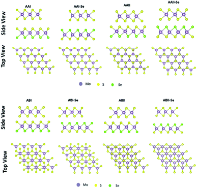 |
| | Fig. 1 Stacking patterns of MoS2/MoSSe heterostructure with different stacking orientations. AA and AB refer to the stacking pattern, whether the two hexagonal lattices are aligned on top of one another or shifted. I and II refer to whether the Mo is is aligned below the metal or the chalcogen atom of JTMDs. Se implies that the Se chalcogen atom is facing the MoS2 monolayer if not mentioned the other chalcogen of the JTMD is facing the MoS2 monolayer. | |
To determine the stability of the hetero-structures and the most favourable stacking pattern for each TMD-JTMD configuration, we calculated the binding energy for all the stacking patterns. This consist of 24 different structures and the results are presented in Table 2.
Table 2 Binding energies (Eb in eV) and stacking pattern of different configuration of MoS2/Janus TMDCs heterostructure
| Heterostructure |
Stacking pattern |
Binding energy Eb (eV) |
| MoS2/MoSSe |
AAI |
−0.006 |
| AAI-Se |
−0.006 |
| AAII |
−0.009 |
| AAII-Se |
−0.011 |
| ABI |
−0.008 |
| ABI-Se |
−0.010 |
| ABII |
−0.009 |
| ABII-Se |
−0.011 |
| MoS2/MoSTe |
AAI |
0.001 |
| AAI-Te |
−0.002 |
| AAII |
−0.003 |
| AAII-Te |
−0.009 |
| ABI |
−0.003 |
| ABI-Te |
−0.006 |
| ABII |
−0.004 |
| ABII-Te |
−0.008 |
| MoS2/WSSe |
AAI |
−0.008 |
| AAI-Se |
−0.009 |
| AAII |
−0.013 |
| AAII-Se |
−0.015 |
| ABI |
−0.012 |
| ABI-Se |
−0.013 |
| ABII |
−0.013 |
| ABII-Se |
−0.015 |
The most stable stacking pattern of the TMD-JTMD, which is the configuration with the most negative binding energy is used for further studies. As shown in Table 2, the stable stacking pattern are the AAII-Se MoSSe, AAII-Te MoSTe, and AAII-Se WSSe heterostructures. The electronic properties, photocatalytic water splitting, and photovoltaic solar cells performance are presented and discussed below.
(b) Electronic properties
The electronic structure calculation of the investigated materials is summarized below in Tables 3 and 4 for the monolayers and heterostructures respectively. Table 3 shows the optimized lattice constant a (Å), band gap (calculated using PBE and HSE06 in eV), work function (φ in eV), valence and conduction band edge relative to the vacuum (EVB & ECB) for the three considered heterostructures. The calculated band gaps are indirect (MoSSe and MoSTe) and direct (MoS2 and WSSe) using PBE functional. The calculated band gap using the HSE06 functional is consistently larger than those determined using the PBE functional for all the considered monolayers.
Table 3 Optimized lattice constant a (Å), band gap (calculated using PBE and HSE06 in eV), work function (φ in eV), valence and conduction band edge relative to the vacuum (EVB & ECB) for the monolayers
| Monolayer |
MoS2 |
MoSSe |
MoSTe |
WSSe |
| a (This study) |
3.19 |
3.26 |
3.260 |
3.26 |
| a (Expet.) |
3.159 [ref. 69] |
— |
— |
— |
| Eg-PBE |
1.74 (dir) |
1.65 (dir) |
1.16 (ind) |
1.77 (dir) |
| Eg-HSE06 |
2.278 |
2.028 |
1.571 |
2.195 |
| Eg-Expet. |
1.9 eV [ref. 68] |
1.68 eV [ref. 70] |
— |
— |
| φ |
6.273 |
5.955 |
5.289 |
5.728 |
| EVB |
−6.273 |
−5.955 |
−5.289 |
−5.728 |
| ECB |
−3.995 |
−3.927 |
−3.718 |
−3.533 |
Table 4 Optimized lattice constant a (Å), band gap (calculated using PBE and HSE06 in eV), work function (φ in eV), valence and conduction band edge relative to the vacuum (EVB & ECB) for the Heterostructures
| Heterostructure |
AAII-Se MoSSe |
AAII-Te MoSTe |
AAII-Se WSSe |
| a |
3.220 |
3.270 |
3.220 |
| Eg-PBE |
1.026 (ind) |
0.303 (ind) |
0.838 (dir) |
| Eg-HSE06 |
1.133 |
0.000 |
0.928 |
| φ |
5.904 |
5.435 |
5.646 |
| EVB |
−6.33 |
−5.90 |
−6.07 |
| ECB |
−3.73 |
−4.47 |
−3.67 |
To the best of our knowledge, two types of Janus layered material have been synthesized thus far, which are the MoSSe and WSSe monolayers. As such, a direct comparison of the evaluated findings with the experimental investigation is not feasible. However, the theoretical method applied yields consistent qualitative results with experimental data. The calculated lattice parameters 3.19, 3.26, 3.26 Å and band gap 2.278, 2.03, 2.2 eV for the pristine MoS2, MoSSe, WSSe, are consistent with available experimental data as presented in Table 3. MoSSe has a lattice constant that falls between MoS2 (3.159 A) and MoSe2 (3.30 A),71,72 which is appropriate given MoSSe's composition.
Table 3 shows the optimized lattice constant a (Å), band gap (calculated using PBE and HSE06 in eV), work function (φ in eV), valence and conduction band edge relative to the vacuum (EVB & ECB) for the three considered heterostructures. The calculated band gaps are indirect (AAII-Se MoSSe and AAII-Te MoSTe) and direct (AAII-Se WSSe) using PBE functional, however with HSE06 we found that the AAII-Se MoSSe and AAII-Se WSSe are semi-conducting whereas the AAII-Te MoSTe is metallic. The AAII-Se MoSSe and AAII-Se WSSe are semiconductor with a band gap value of 1.33 eV and 0.928 eV respectively. These two configurations are further considered as possible photocatalyst and photovoltaic material. The band structure diagram using HSE06 hybrid functional are presented as Fig. 2 for these heterostructures.
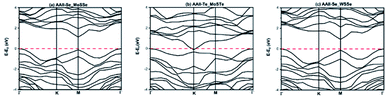 |
| | Fig. 2 Band Structure of AAII-Se MoSSe, AAII-Te MoSTe, and AAII-Se WSSe. | |
(c) Photocatalytic water splitting
Photocatalytic water splitting has received a lot of interest as an energy-efficient and environmentally friendly way to create hydrogen.57,58 The overall photocatalytic water splitting process can proceed as presented in eqn (2):| |
 | (2) |
where ΔE0 is the equilibrium potential at standard conditions. The oxidation and reduction half-cell reactions are involved in the photoelectrochemical (PCE) path to water splitting and is presented below:| | |
Oxidation ∼ 2H2O(l) = O2(g) + 4H+(aq) + 4e−
| (3) |
and| | |
Reduction ∼ 4H+(aq) + 4e− = 2H2(g)
| (4) |
An efficient photocatalyst should have the conduction band (CB) potential greater than the H+/H2 potential for the reduction reaction (eqn (4)) to occur. While the valence band (VB) energy level should be greater than the OH−/O2 potential for the oxidation reaction (eqn (3)) to occur. Thus, the bandgap criterion for photocatalysis corresponds to the minimal potential difference, which is 1.23 eV.59 The conventional water redox potentials in terms of vacuum are 4.44 eV for reduction (H+/H2) and 5.67 eV for oxidation (H2O/O2).60
The band edge position of the heterostructures of AAII-Se MoSSe and AAII-Se WSSe for water splitting is shown in Fig. 2.
As demonstrated in Fig. 3a, the band edge positions of the AAII-Se MoSSe and AAII-Se WSSe heterostructures do not straddle the water redox potentials at pH = 0. This means that these heterostructures fail to meet the thermodynamic criteria of an efficient photocatalyst for splitting water into hydrogen and oxygen molecules. However, AAII-Se MoSSe is a good photocatalyst for the oxygen evolution reaction as shown in the plot, and AAII-Se WSSe is as well if the band edge is slightly modified. As we know, strain engineering is a viable method for tuning the band gap and band-edge positions, as demonstrated by several research for various materials. In future studies, we would demonstrate the effect of strain on the conduction band edge to make this heterostructure possible for overall water splitting.
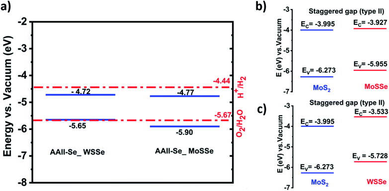 |
| | Fig. 3 (a) Band edge positions of the two heterojunctions for photocatalytic water splitting. The redox potential of water splitting at pH = 0 is shown by the red dashed line. (b) Schematic representation of type II band alignment AAII-Se MoSSe heterostructure. (c) Schematic representation of type II band alignment AAII-Se WSSe heterostructure. | |
Overall, the good catalytic performance obtained can be attributed to the following: (a) several intrinsic features of the heterostructure remain unchanged because of the weak van der Waals interlayer interaction. As a result, the good catalytic performance of MoS2 is transferred to some of these heterostructures. (b) The heterostructure overcomes a notable drawback of a single MoS2 monolayer, which is rapid charge recombination resulting in improved catalytic performance. The redox potential versus light absorption in the semiconductor is an irreconcilable contradiction for photocatalytic water-splitting. A small band gap is beneficial for the high light absorption, in contrast a large bandgap is essential for a high redox potential for water splitting. The balance is hard to be attain in single monolayers but can be addressed in vdW heterostructures. Thus, these vdW heterostructures combines layers with different properties such as lattice parameter, electronic band gaps, etc. resulting in exciting new characteristics. The combination of MoS2 and Janus monolayers shows some of these attributes as discussed and evaluated in the current study.
Considering, the band gap alignment, we obtained that both structures exhibit type II alignment, as illustrated in Fig. 3b and c. This allows for efficient charge carrier separation and increases the photocatalytic water splitting activity. As indicated in the introduction, the short lifetimes of photogenerated electrons that easily recombine with holes jeopardize MoS2's suitability as a photocatalyst. This issue is overcome, however, by forming a type-II heterostructure with MoSSe and WSSe.
(d) Photovoltaic solar cells
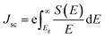
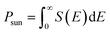
Heterostructures based on atomically thin semiconductors are a promising developing technology for achieving ultrathin and lightweight photovoltaic solar cells on flexible substrates.61 The stable two heterostructure configurations considered have reasonable band gap and exhibit type-II band alignment, which is critical for photovoltaic energy conversion62 making them a good candidate for photovoltaic applications. Thus, the performance of these heterostructure for photovoltaic applications is evaluated. To investigate the solar cell storage or conversion performance of these anticipated vdW hetero-structured materials, we used the following equation63 to calculate the maximum power conversion efficiency (PCE) (η). η which is expressed below is the most essential metric describing a photovoltaic device.| |
 | (5) |
Using
| |
 | (7) |
| |
 | (8) |
where FF denotes the fill factor,
Voc denotes the maximum open-circuit voltage (
Eg −
Eloss),
Jsc denotes the maximum short-circuit current density, and
S(
E) is calculated using the NREL AM1.5 dataset. The bandgap energy is denoted by
Eg. According to previous reports, the fill factors in 2D heterostructure photovoltaic structures are typically in the range of 0.3–0.5,
61 so we take this value, and energy losses
Eloss can be assumed to be 0.3.
64 Because a previous experimental research discovered a fill factor of 0.57 for a MoS
2/p-Si heterostructure.
65 We use this as our fill factor because it is the only experimental article that the authors are aware of that reports a fill factor for a TMD. Using the equation presented above, the computed PCE values for AAII-Se MoSSe and AAII-Se WSSe are (7.289–12.15%) and (5.62–9.37%) respectively, which are much better than the results for MoS
2/p-Si (5.23%)
66 WSe
2–MoS
2 (2.56%).
67
Conclusions
Using first-principles calculations, we studied the structural and electrical characteristics of the MoS2/Janus TMDs van der Waals heterostructure. The most energetically stable stacking patterns of AAII-Se MoSSe and AAII-Se WSSe exhibit type II band gap alignment as well as indirect and direct band gap alignment. At pH = 0, the heterostructures have no acceptable band edge positions for overall water splitting but are good for the oxygen evolution reaction. Many investigations for various materials have demonstrated that strain engineering is a viable method for tuning the band gap and band-edge positions therefore there is a chance vary the position of the band edges and make the heterostructures active for overall water splitting applications. Furthermore, the power conversion efficiency of both heterostructures is comparable to and greater than the value published for similar 2D van der Waals heterostructures. Overall, the type-II heterostructure and high-power conversion efficiency imply that the vdW heterostructure we studied has a lot of promise for usage in photovoltaic devices and, with minor modifications, photocatalytic devices.
Conflicts of interest
There are no conflicts to declare.
Acknowledgements
This work was substantially sponsored by funding from Addis Abeba University through a thematic project (Grant No. RD/LT-095/2019). We also gratefully acknowledge Dr Tekalign T. Debela, Postdoctoral Associate at the University of Oregon, for providing insight and expertise that considerably aided the research. The authors thank the Centre for High Performance Computing (CHPC) in Cape Town, South Africa, for the computational resources used in this study. KOO acknowledges the HySA Infrastructure Centre of Competence, Faculty of Engineering, North-West University for their financial support.
References
- G. A. Asres, A. Dombovari, T. Sipola, R. Puskás, A. Kukovecz, Z. Kónya, A. Popov, J. F. Lin, G. S. Lorite, M. Mohl, G. Toth, A. Lloyd Spetz and K. Kordas, Sci. Rep., 2016, 6, 1–7 CrossRef PubMed.
- K. O. Obodo, C. N. M. Ouma, J. T. Obodo and M. Braun, Phys. Chem. Chem. Phys., 2017, 19, 19050–19057 RSC.
- K. S. Novoselov, D. Jiang, F. Schedin, T. J. Booth, V. V Khotkevich, S. V Morozov and A. K. Geim, Proc. Natl. Acad. Sci. U. S. A., 2005, 102, 10451 CrossRef CAS PubMed.
- K. F. Mak, C. Lee, J. Hone, J. Shan and T. F. Heinz, Phys. Rev. Lett., 2010, 105, 2–5 CrossRef PubMed.
- B. Radisavljevic, A. Radenovic, J. Brivio, V. Giacometti and A. Kis, Nat. Nanotechnol., 2011, 6, 147–150 CrossRef CAS PubMed.
- X. Wang, K. Maeda, A. Thomas, K. Takanabe, G. Xin, J. M. Carlsson, K. Domen and M. Antonietti, Nat. Mater., 2009, 8, 76–80 CrossRef CAS PubMed.
- X. Wang, K. Maeda, X. Chen, K. Takanabe, K. Domen, Y. Hou, X. Fu and M. Antonietti, J. Am. Chem. Soc., 2009, 131, 1680–1681 CrossRef CAS PubMed.
- M. Zhang, Q. Wu, F. Zhang, L. Chen, X. Jin, Y. Hu, Z. Zheng and H. Zhang, Adv. Opt. Mater., 2019, 7, 1–18 Search PubMed.
- S. Guo, Y. Zhang, Y. Ge, S. Zhang, H. Zeng and H. Zhang, Adv. Mater., 2019, 31, 1–19 Search PubMed.
- K. O. Obodo, C. N. M. Ouma, P. M. Modisha and D. Bessarabov, Appl. Surf. Sci., 2020, 529, 147186 CrossRef CAS.
- I. C. Onyia, S. O. Ezeonu, D. Bessarabov and K. O. Obodo, Comput. Mater. Sci., 2021, 197, 110613 CrossRef CAS.
- X. Jiang, A. V. Kuklin, A. Baev, Y. Ge, H. Ågren, H. Zhang and P. N. Prasad, Phys. Rep., 2020, 848, 1–58 CrossRef CAS.
- Z. Lin, B. R. Carvalho, E. Kahn, R. T. Lv, R. Rao, H. Terrones, M. A. Pimenta and M. Terrones, 2D Mater., 2016, 3, 022002 CrossRef.
- N. Lu, H. Guo, L. Li, J. Dai, L. Wang, W.-N. Mei, X. Wu and X. C. Zeng, Nanoscale, 2014, 6, 2879–2886 RSC.
- K. Koåmider and J. Fernández-Rossier, Phys. Rev. B: Condens. Matter Mater. Phys., 2013, 87, 2–5 Search PubMed.
- A. Vargas, F. Liu, C. Lane, D. Rubin, I. Bilgin, Z. Hennighausen, M. Decapua, A. Bansil and S. Kar, Sci. Adv., 2017, 3(7) DOI:10.1126/sciadv.1601741.
- C. Tan, J. Chen, X. J. Wu and H. Zhang, Nat. Rev. Mater., 2018, 3, 1–13 CrossRef.
- Y. Zhang, C. K. Lim, Z. Dai, G. Yu, J. W. Haus, H. Zhang and P. N. Prasad, Phys. Rep., 2019, 795, 1–51 CrossRef CAS.
- J. Low, J. Yu, M. Jaroniec, S. Wageh and A. A. Al-Ghamdi, Adv. Mater., 2017, 29, 1–20 CrossRef PubMed.
- L. Ju, M. Bie and X. Zhang, et al., Front. Phys., 2017, 16, 13201 CrossRef.
- Y. Boyjoo, H. Sun, J. Liu, V. K. Pareek and S. Wang, Chem. Eng. J., 2017, 310, 537–559 CrossRef CAS.
- J. Zhang, G. Xiao, F. X. Xiao and B. Liu, Mater. Chem. Front., 2017, 1, 231–250 RSC.
- C. Jiang, K. Y. Lee, C. M. A. Parlett, M. K. Bayazit, C. C. Lau, Q. Ruan, S. J. A. Moniz, A. F. Lee and J. Tang, Appl. Catal., A, 2016, 521, 133–139 CrossRef CAS.
- Z. Jiang, Z. Y. Zhang, W. Shangguan, M. A. Isaacs, L. J. Durndell, C. M. A. Parlett and A. F. Lee, Catal. Sci. Technol., 2016, 6, 81–88 RSC.
- S. Kumar, C. M. A. Parlett, M. A. Isaacs, D. V. Jowett, R. E. Douthwaite, M. C. R. Cockett and A. F. Lee, Appl. Catal., B, 2016, 189, 226–232 CrossRef CAS.
- E. Benavente, F. Durán, C. Sotomayor-Torres and G. González, J. Phys. Chem. Solids, 2018, 113, 119–124 CrossRef CAS.
- R. Kumar, D. Das and A. K. Singh, J. Catal., 2018, 359, 143–150 CrossRef CAS.
- E. Singh and H. S. Nalwa, J. Nanosci. Nanotechnol., 2015, 15, 6237–6278 CrossRef CAS PubMed.
- E. Singh and H. S. Nalwa, RSC Adv., 2015, 5, 73575–73600 RSC.
- E. Singh and H. S. Nalwa, Sci. Adv. Mater., 2015, 7, 1863–1912 CrossRef CAS.
- R. Li, Y. Cheng and W. Huang, Small, 2018, 14, 1802091 CrossRef PubMed.
- Y. C. Cheng, Z. Y. Zhu, W. B. Mi, Z. B. Guo and U. Schwingenschlögl, Phys. Rev. B: Condens. Matter Mater. Phys., 2013, 87, 2 Search PubMed.
- K. O. Obodo, C. N. M. Ouma, J. T. Obodo, M. Braun and D. Bessarabov, Comput. Condens. Matter, 2019, 21, e00419 CrossRef.
- S. Wi, H. Kim, M. Chen, H. Nam, L. J. Guo, E. Meyhofer and X. Liang, ACS Nano, 2014, 8, 5270–5281 CrossRef CAS PubMed.
- J. Zhang, M. Zhang, R. Q. Sun and X. Wang, Angew. Chem., Int. Ed., 2012, 51, 10145–10149 CrossRef CAS PubMed.
- V. O. Özçelik, J. G. Azadani, C. Yang, S. J. Koester and T. Low, Phys. Rev. B, 2016, 94, 035125 CrossRef.
- S. Wang, C. Ren, H. Tian, J. Yu and M. Sun, Phys. Chem. Chem. Phys., 2018, 20, 13394–13399 RSC.
- M. Bernardi, M. Palummo and J. C. Grossman, Nano Lett., 2013, 13, 3664–3670 CrossRef CAS PubMed.
- F. Li, W. Wei, P. Zhao, B. Huang and Y. Dai, J. Phys. Chem. Lett., 2017, 8(23), 5959–5965, DOI:10.1021/acs.jpclett.7b02841.
- Y. Ji, M. Yang, H. Lin, T. Hou, L. Wang, Y. Li and S. T. Lee, J. Phys. Chem. C, 2018, 122, 3123–3129 CrossRef CAS.
- A. Y. Lu, H. Zhu, J. Xiao, C. P. Chuu, Y. Han, M. H. Chiu, C. C. Cheng, C. W. Yang, K. H. Wei, Y. Yang, Y. Wang, D. Sokaras, D. Nordlund, P. Yang, D. A. Muller, M. Y. Chou, X. Zhang and L. J. Li, Nat. Nanotechnol., 2017, 12, 744–749 CrossRef CAS PubMed.
- J. Zhang, S. Jia, I. Kholmanov, L. Dong, D. Er, W. Chen, H. Guo, Z. Jin, V. B. Shenoy, L. Shi and J. Lou, ACS Nano, 2017, 11, 8192–8198 CrossRef CAS PubMed.
- P. E. Blöchl, Phys. Rev. B, 1994, 50, 17953 CrossRef PubMed.
- J. P. Perdew, K. Burke and M. Ernzerhof, Phys. Rev. Lett., 1996, 77(4), 3865 CrossRef CAS PubMed.
- B. Ghosh, S. Nahas, S. Bhowmick and A. Agarwal, Phys. Rev. B: Condens. Matter Mater. Phys., 2015, 91, 1–6 Search PubMed.
- B. J. Wang, X. H. Li, R. Zhao, X. L. Cai, W. Y. Yu, W. Bin Li, Z. S. Liu, L. W. Zhang and S. H. Ke, J. Mater. Chem. A, 2018, 6, 8923–8929 RSC.
- J. Heyd, G. E. Scuseria and M. Ernzerhof, J. Chem. Phys., 2003, 118, 8207–8215 CrossRef CAS.
- A. V. Krukau, O. A. Vydrov, A. F. Izmaylov and G. E. Scuseria, J. Chem. Phys., 2006, 125, 224106 CrossRef PubMed.
- A. Miralrio, E. Rangel Cortes and M. Castro, Appl. Surf. Sci., 2018, 455, 758–770 CrossRef CAS.
- M. Farmanbar and G. Brocks, Phys. Rev. B, 2016, 93, 1–12 Search PubMed.
- S. Ahmad, I. Ahmad, N. Van and B. Amin, RSC Adv., 2020, 10, 38114–38119 RSC.
- M. Yagmurcukardes, C. Sevik and F. M. Peeters, Phys. Rev. B, 2019, 100, 1–8 Search PubMed.
- X. Yang, D. Singh, Z. Xu, Z. Wang and R. Ahuja, J. Mater. Chem. C, 2019, 7, 12312–12320 RSC.
- H. G. Abbas, T. T. Debela, J. R. Hahn and H. S. Kang, J. Phys. Chem. C, 2021, 125, 7458–7465 CrossRef CAS.
- T. V. Vu, N. V. Hieu, H. V. Phuc, N. N. Hieu, H. D. Bui, M. Idrees, B. Amin and C. V. Nguyen, Appl. Surf. Sci., 2020, 507, 145036 CrossRef CAS.
- T. A. Alrebdi and B. Amin, Chem. Phys., 2021, 549, 111252 CrossRef CAS.
- K. Maeda, K. Teramura, D. Lu, T. Takata, N. Saito, Y. Inoue and K. Domen, Nature, 2006, 440, 295 CrossRef CAS PubMed.
- S. Y. Reece, J. A. Hamel, K. Sung, T. D. Jarvi, A. J. Esswein, J. J. H. Pijpers and D. G. Nocera, Science, 2011, 334, 645–648 CrossRef CAS PubMed.
- E. L. Miller, Energy Environ. Sci., 2015, 8, 2809–2810 RSC.
- J. Kang, S. Tongay, J. Zhou, J. Li and J. Wu, Appl. Phys. Lett., 2013, 102, 22–25 Search PubMed.
- M. M. Furchi, F. Höller, L. Dobusch, D. K. Polyushkin, S. Schuler and T. Mueller, npj 2D Mater. Appl., 2018, 2, 1–7 CrossRef.
- J. Kang, H. Sahin and F. M. Peeters, J. Phys. Chem. C, 2015, 119, 9580–9586 CrossRef CAS.
- M. R. Filip, C. Verdi and F. Giustino, J. Phys. Chem. C, 2015, 119, 25209–25219 CrossRef CAS.
- H. J. Snaith, Adv. Funct. Mater., 2010, 20, 13–19 CrossRef CAS.
- S. K. Pradhan, B. Xiao and A. K. Pradhan, Sol. Energy Mater. Sol. Cells, 2016, 144, 117–127 CrossRef CAS.
- M. L. Tsai, S. H. Su, J. K. Chang, D. S. Tsai, C. H. Chen, C. I. Wu, L. J. Li, L. J. Chen and J. H. He, ACS Nano, 2014, 8, 8317–8322 CrossRef CAS PubMed.
- M. L. Tsai, M. Y. Li, J. R. D. Retamal, K. T. Lam, Y. C. Lin, K. Suenaga, L. J. Chen, G. Liang, L. J. Li and J. H. He, Adv. Mater., 2017, 29, 1–7 Search PubMed.
- K. F. Mak, C. Lee, J. Hone, J. Shan and T. F. Heinz, Phys. Rev. Lett., 2010, 105(13), 136805 CrossRef PubMed.
- N. Bandaru, R. S. Kumar, D. Sneed, O. Tschauner, J. Baker, D. Antonio, S. Luo, T. Hartmann, Y. Zhao and R. Venkat, J. Phys. Chem. C, 2014, 118(6), 3230–3235 CrossRef CAS.
- Y. N. Wen, M. G. Xia and S. L. Zhang, Comput. Mater. Sci., 2018, 152, 20–27 CrossRef CAS.
- L. Kou, A. Du, C. Chen and T. Frauenheim, Nanoscale, 2014, 6(10), 5156–5161 RSC.
- Q. Yue, Z. Shao, S. Chang and J. Li, Nanoscale Res. Lett., 2013, 8(1), 1–7 CrossRef PubMed.
|
| This journal is © The Royal Society of Chemistry 2022 |
Click here to see how this site uses Cookies. View our privacy policy here. 
 Open Access Article
 This Open Access Article is licensed under a Creative Commons Attribution-Non Commercial 3.0 Unported Licence
 cd and
Georgies A. Asres
cd and
Georgies A. Asres


