
 Open Access Article
 This Open Access Article is licensed under a Creative Commons Attribution-Non Commercial 3.0 Unported Licence
High-temperature ionic logic gates composed of an ionic rectifying solid–electrolyte interface
Takashi Nakamura *a,
Miri Hondab,
Yuta Kimuraa and
Koji Amezawaa
*a,
Miri Hondab,
Yuta Kimuraa and
Koji Amezawaa
aInstitute of Multidisciplinary Research for Advanced Materials, Tohoku University, 2-1-1, Katahira, Aoba-Ku, Sendai, 980-8577, Japan. E-mail: takashi.nakamura.e3@tohoku.ac.jp
bGraduate School of Engineering, Tohoku University, 6-6-1 Aramaki-Aoba, Aoba-ku, Sendai, 980-8579, Japan
First published on 23rd June 2022
Abstract
Direct data collection from extremely high temperature environments is vitally important for the progress of industrial technologies such as combustion-engines, turbines and furnaces for various purposes. However, present semiconductor-based information devices are not suitable for such high-temperature applications due to thermal excitation of electronic carriers. Herein, we demonstrate high-temperature ionic AND and OR logic gates composed of the oxide-ion-conducting yttria stabilized zirconia (YSZ) and the mixed oxide-ion and electron conducting La2NiO4+δ as an ultra-high temperature information device. The ionic AND and OR gates developed in this work exhibited proper and stable electrical responses at 1073 K. The ionic logic gates shown in this work are promising demonstrations for robust information devices in extreme environments.
Introduction
Machine-learning and artificial intelligence are recognized as powerful tools enabling efficient and accurate estimation/analysis from large-scale data.1,2 For such data analysis technologies, the collection of reliable and high-quality data set is essentially important. For example, direct data collection from extremely high temperature environments such as combustion-engines, turbines and furnaces will provide fruitful information for efficient device operation and mass production. Moreover, such high temperature data collection technologies will also contribute to the progress of fundamental natural sciences like an exploration of the earth's core and fixed stars. To achieve direct data collection from extreme environments, a new type of logic gate which can stably work at high temperatures is necessary because conventional Si-based devices are not available at high temperatures due to thermal excitation of electrons. Instead of Si-based semiconductors, wide band gap semiconductors such as SiC, GaN, AlN and diamond have been proposed for high temperature applications and widely studied.3–8 Although these devices work properly at relatively high temperatures, degradation due to thermal excitation of electron is inevitable in semiconductor-based devices. In this work, we propose the utilization of ceramic-based ionic conductors for the realization of the ultra-high temperature data collection technology.As an analogy of the p–n junction of semiconductor devices, an ionic depletion layer is expected to be formed at the junction of a cation conductor and an anion conductor by the recombination of mobile anions and cations, and such a junction will exhibit nonlinear current–voltage characteristics. Ionic rectification at the heterojunction of an anion exchange membrane and cation exchange membrane was firstly reported by Lovreček et al.9 The bilayer membrane structure composed of anion and cation conductors are called bipolar membranes, and so far, many types of bipolar membrane and its application devices have been proposed such as ionic logic gates,10–13 electrodialysis and separations,14–16 electrolysis,17,18 sensors19 and power generations.20,21 Although bipolar membranes exhibit strong ionic rectification, they are not available at high temperatures due to thermal decomposition of the components. Instead of polymer-based materials, ceramics-based solid ion conductors are promising materials for high temperature applications. So far, only a few works have been reported for ionic rectification at solid electrolyte junctions while the underlying concept is the same with the bipolar membranes. Fernandes et al. demonstrated a very weak nonlinear current–voltage relationship at the interface of two dissimilar fluoride ion conductors, Na doped PbF2 which has positively charged fluoride vacancies ( ) and La doped PbF2 which has negatively charged interstitial fluoride ions (
 ).22 They suggested the formation of an ionic depletion layer at the junction by the recombination of
  and
and  . Similarly, weak ionic rectification was reported at the solid electrolyte junctions of oxygen vacancy (
 ) conducting yttria stabilized zirconia (YSZ) and interstitial oxygen (
 ) conducting La doped PbWO423 and the O2− conducting YSZ and the H+ conducting SrZrO3.24
In this study, the ionic diode was fabricated from YSZ and the mixed electron and O2− conducting La2NiO4+δ (LNO), because their compatibility at high temperatures above 873 K was confirmed as a solid oxide fuel cell cathode.25 YSZ has positively charged oxygen vacancies as an ionic carrier, and LNO has negatively charged interstitial oxygen as an ionic carrier as well as mobile electrons. In order to increase the area of the heterojunction and enhance apparent rectifying properties, a YSZ/LNO composite layer was inserted between YSZ and LNO layers like a bulk heterojunction of organic photovoltaic cells.21,26 The prototype of the high-temperature ionic AND and OR gates was constructed from the YSZ/LNO heterojunction, and its electrical responses were tested.
Experimental
Commercial yttria stabilized zirconia (TZ-8Y, Tosoh Ceramics Co., Ltd) and La2NiO4+δ (KCM Corp.) powders were pressed into the disk shape and sintered at 1673 K to obtain dense YSZ and LNO pellets. YSZ and LNO powders were mixed with the organic solvent (TMS-1, TANAKA Kikinzoku Kogyo K.K.) and printed on the YSZ disk by the screen-printing machine (MEC-2400-E, Mitani Electronics Corp., #200 mesh). The composite layer was fabricated on the YSZ pellet by sintering the above-mentioned cell at 1473 K. The half-cell was fabricated by placing Porous Pt current electrodes on YSZ and LNO pellets, and Pt voltage electrodes on the side-face of each pellet. YSZ and LNO half-cells were touched and mechanically pressed to form the YSZ/LNO ionic diode. The current–voltage characteristics of the YSZ/LNO ionic diode was evaluated by potentio/galvanostat (VersaSTAT 4, Princeton Applied Research and SP-200, Bio Logic) at 1073 K in O2–Ar gas-mixtures by applying stepwise voltage in the range between −2 to 2 V. High-temperature ionic AND and OR gates were fabricated from the ionic diode composed of the YSZ/LNO heterojunction in which the input terminals A, B and the output terminal were prepared. The electrical responses of the logic gates were measured at 1073 K in 100 ppm O2–Ar by the multi-channel potentio/galvanostat (VSP, Bio Logic). The input voltage signals for the ionic OR gate was 0.5 V and that for the ionic AND gate was 1.0 V.Results and discussion
Electric responses of the YSZ/LNO heterojunction
For the fabrication of high-temperature ionic logic gates, the ionic rectifying YSZ/LNO interface was investigated. Schematic illustration and a SEM image picture of the YSZ/LNO ionic diode are shown in Fig. 1. Well-mixed composite layer was fabricated between YSZ and LNO layers as designed. Voltage loss owing to supply and exhaust of oxide ion at the current electrodes was eliminated by applying 4 terminal measurement in this work, and therefore, obtained current–voltage characteristics represent electrical response of the heterojunction. As summarized in Fig. 2, the YSZ/LNO heterojunction exhibited nonlinear asymmetric current–voltage relationship. The forward current was observed when YSZ was polarized negatively and LNO was polarized positively, and reverse current was observed by the opposite bias. The observed forward/reverse relation was opposite to that due to the ionic depletion layer. If the ionic depletion layer is formed at the YSZ/LNO heterojunction, the forward current should be obtained when positive and negative voltage were applied to the YSZ side and the LNO side, respectively, because ionic carriers in each component ( in YSZ and
  in LNO) move to the junction and the length of the ionic depletion layer decreases.
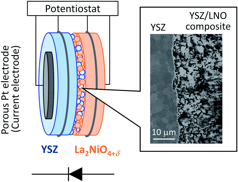 | ||
| Fig. 1 Schematic illustration of the YSZ/LNO diode and the backscattered electron image of the cross section of the YSZ/LNO composite layer. | ||
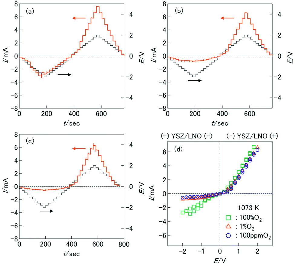 | ||
| Fig. 2 Transient current–voltage characteristics of the YSZ/LNO heterojunction at 1073 K in various P(O2) atmosphere, (a) 100% O2, (b) 1% O2-Ar and (c) 100 ppmO2-Ar. (d) Steady state current–voltage characteristics of the YSZ/LNO heterojunction forward and reverse bias are also shown on the top. | ||
The transient current responses of the YSZ/LNO heterojunction were investigated and summarized in Fig. 3a. Steady-state current was obtained within 10 seconds after the voltage application. Although the observed transient responses are comparable to reported bipolar membranes,10,11 this is much slower than conventional semiconductor-based diodes. Despite slow responsiveness, stable current rectification of the YSZ/LNO heterojunction was observed at high temperature (1073 K). Current rectification of the YSZ/LNO heterojunction was kept after 2000 times voltage switching (Fig. 3b). As shown, the forward current gradually increased and the reverse current was mostly constant with bias switch, and consequently, the rectification ratio (Rrec), the forward current over the reverse current, increased upon voltage cycling. By the modification of the composite layer, the strongest rectification ratio (Rrec = 23.2 @ ± 2 V) was achieved at 1073 K in 100 ppm O2–Ar.
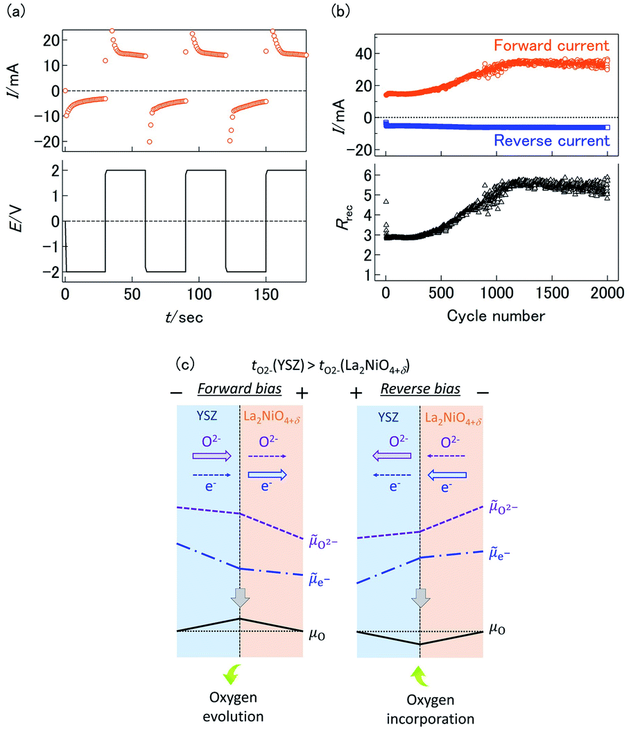 | ||
| Fig. 3 (a) Transient current responses and (b) cycle stability of current rectification under ±2 V at 1073 K in 100 ppmO2-Ar. (c) Schematic picture of the mass/charge transport and potential distribution near the YSZ/LNO heterojunction under polarization. | ||
Possible cause of ionic rectification at the YSZ/LNO heterojunction
The inconsistency of forward/reverse direction strongly suggests that the ionic rectification at the YSZ/LNO heterojunction was not caused by ionic depletion layer. The alternative cause of the current asymmetricity is the perturbation of oxygen chemical potential at the heterojunction. According to charge and mass transport through the interface of a bilayer solid electrolyte,27–29 the difference of ionic transference number (tion = σion/(σion + σel) where σion and σel represent the ionic conductivity and electronic conductivity, respectively) of each solid electrolyte may result in the mismatch of the ionic current and the electronic current at the junction while total charge flux (ionic current + electronic current) is constant under steady-state condition. In this situation, the mismatch of ionic current and electronic current is balanced by the electrochemical reaction at the solid electrolyte junction which is essentially caused by the perturbation of chemical potential at the interface.29 The schematic mass/charge transport and potential profile in the YSZ/LNO bilayer system is illustrated in Fig. 3c. Here, μO,![[small mu, Greek, tilde]](https://www.rsc.org/images/entities/i_char_e0e0.gif) O2− and e− represent the chemical potential of oxygen, the electrochemical potential of oxide ion and the electrochemical potential of electron, respectively. Under the open circuit condition, the cell is equilibrated with the gas phase and μO in the cell is equal of that in the gas phase (dashed black line in Fig. 3c). Under the steady-state biased condition, steep e− gradient and moderate O2− gradient are formed in the YSZ and moderate e− gradient and steep O2− gradient are formed in LNO, because the relation of transport numbers, tO2−(YSZ) > tO2−(LNO), is kept. From local equilibrium (μO = O2− − 2e−), μO at the junction increases compared with that in the gas-phase under the observed forward bias condition (−/YSZ/LNO/+). The increase of μO at the heterojunction can promote oxygen evolution reaction, 2O2−(YSZ/LNO) → O2(gas) + 4e−(LNO), at the junction. On the contrary, under the observed reverse bias condition (+/YSZ/LNO/−), the (electro)chemical potential shifts opposite direction. μO at the junction decreases from the initial state and electrolytic incorporation of oxygen, O2(gas) + 4e−(LNO) → 2O2−(YSZ/LNO), is facilitated under the reverse bias. The difference of the reaction rate of oxygen incorporation and oxygen evolution can cause ionic current rectification. This hypothesis was verified by the P(O2) dependence of the current asymmetricity (Fig. 2d). As shown in the figure, reverse current due to oxygen incorporation decreased rapidly with decreasing P(O2) in the gas phase, while forward current due to oxygen evolution was almost constant regardless of P(O2) in gas phase. Consequently, Rrec increase with decreasing P(O2). The observed P(O2) dependence can be explained that oxygen incorporation was hindered by insufficient oxygen supply from gas phase in low P(O2) condition while oxygen evolution proceeds regardless of the atmospheric condition. At the YSZ/LNO heterojunction, the contribution of electrolytic reactions is stronger than that of the ionic depletion layer. Although apparent ionic rectification at the YSZ/LNO heterojunction was caused by electrolytic reactions, it is worth mentioning that present results do not deny the presence of ionic depletion layer at the solid–electrolyte junction.
O2− and e− represent the chemical potential of oxygen, the electrochemical potential of oxide ion and the electrochemical potential of electron, respectively. Under the open circuit condition, the cell is equilibrated with the gas phase and μO in the cell is equal of that in the gas phase (dashed black line in Fig. 3c). Under the steady-state biased condition, steep e− gradient and moderate O2− gradient are formed in the YSZ and moderate e− gradient and steep O2− gradient are formed in LNO, because the relation of transport numbers, tO2−(YSZ) > tO2−(LNO), is kept. From local equilibrium (μO = O2− − 2e−), μO at the junction increases compared with that in the gas-phase under the observed forward bias condition (−/YSZ/LNO/+). The increase of μO at the heterojunction can promote oxygen evolution reaction, 2O2−(YSZ/LNO) → O2(gas) + 4e−(LNO), at the junction. On the contrary, under the observed reverse bias condition (+/YSZ/LNO/−), the (electro)chemical potential shifts opposite direction. μO at the junction decreases from the initial state and electrolytic incorporation of oxygen, O2(gas) + 4e−(LNO) → 2O2−(YSZ/LNO), is facilitated under the reverse bias. The difference of the reaction rate of oxygen incorporation and oxygen evolution can cause ionic current rectification. This hypothesis was verified by the P(O2) dependence of the current asymmetricity (Fig. 2d). As shown in the figure, reverse current due to oxygen incorporation decreased rapidly with decreasing P(O2) in the gas phase, while forward current due to oxygen evolution was almost constant regardless of P(O2) in gas phase. Consequently, Rrec increase with decreasing P(O2). The observed P(O2) dependence can be explained that oxygen incorporation was hindered by insufficient oxygen supply from gas phase in low P(O2) condition while oxygen evolution proceeds regardless of the atmospheric condition. At the YSZ/LNO heterojunction, the contribution of electrolytic reactions is stronger than that of the ionic depletion layer. Although apparent ionic rectification at the YSZ/LNO heterojunction was caused by electrolytic reactions, it is worth mentioning that present results do not deny the presence of ionic depletion layer at the solid–electrolyte junction.
High temperature ionic AND and OR gates
For the demonstration of high-temperature ionic logic gates, the ionic AND and OR gates were fabricated from YSZ/LNO diodes (Fig. 4a and b). The pictures of the ionic diode and the ionic OR gate are shown in Fig. 4c. Ideal AND and OR gates and their responses (truth table) are summarized in the Table 1 where 1 represents high voltage state and 0 represents low voltage state in the table. The electric response of the ionic logic gates was tested at 1073 K in 100 ppm O2–Ar atmosphere, and 60 voltage cycles of (0, 0), (1, 0), (0, 1) and (1, 1) were examined. Although small differences were observed in the reproducibility test for 3–5 distinct devices, reasonable AND and OR responses were confirmed. The best responses obtained in this work were summarized in Fig. 5. In both the ionic AND and OR gates, the observed voltage output reached steady state within 1 min after applying the input voltages. The observed gradual change of electric responses is considered to be mainly attributed to the slow kinetics of the electrolytic oxygen evolution/incorporation reactions at the YSZ/LNO heterojunction. Such a slow response is not desirable for the practical logic element, however, both the ionic logic gates showed reasonable electric responses as the AND and OR gates. When (1, 0), (0, 1) and (0, 0) were inputted to the ionic AND gate (the input voltage was 1.0 V), the output voltage was below 0.33 V, while the output voltage was 0.97 V when (1, 1) was inputted. This behavior is consistent with the truth table of the ideal AND gate. Similarly, when (1, 0), (0, 1) and (1, 1) were inputted (actual input voltage was 0.5 V) to the ionic OR gate, the output voltage was higher than 0.1 V, while the output voltage was 0 V when (0, 0) was inputted.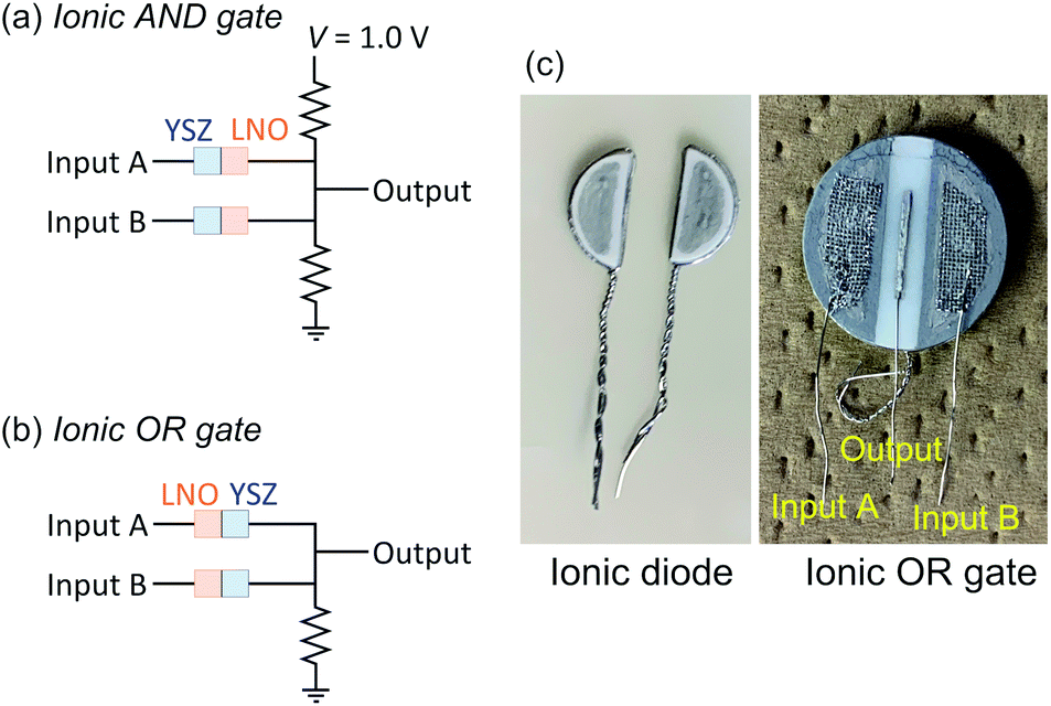 | ||
| Fig. 4 Schematic images of the ionic (a) AND and (b) OR gates composed of the YSZ/LNO heterojunction. (c) Pictures of YSZ/LNO diodes used for the ionic logic gates and the ionic OR gate. The YSZ/LNO composite layer was covered by Pt current collectors. | ||
| Input | Output of AND gate | Output of OR gate |
|---|---|---|
| (0, 0) | 0 | 0 |
| (1, 0) | 0 | 1 |
| (0, 1) | 0 | 1 |
| (1, 1) | 1 | 1 |
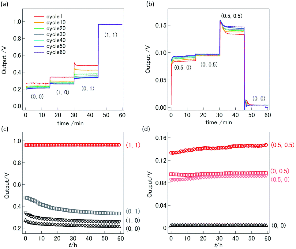 | ||
| Fig. 5 Transient output voltage change of the ionic (a) AND gate and (b) OR gates at 1073 K. Long-term stability of electric responses of the ionic (c) AND gate and (d) OR gate at 1073 K in 100 ppm O2–Ar atmosphere. Input voltages are shown in parentheses. | ||
The voltage difference between high voltage state and low voltage state was smaller than expected, especially in the ionic OR gate. A possible cause is the large potential drop due to ohmic resistance of the YSZ substrate. The influence of the ohmic resistance of the substrate was semi-quantitatively evaluated by the circuit simulator.30 Fig. 6a and b show the schematic illustration of the cell configuration of the ionic OR gate and the corresponding equivalent circuit. In the figure, R1 and R2 represent the ohmic resistance along the lateral direction and R3 represents the ohmic resistance along the depth direction of the substrate. To investigate the influence of ohmic resistance on electric response, the output of the OR gate was calculated under the assumption that R1 = R2 = Rohm are variable and R3 was fixed to 100 Ω. With increasing Rohm, the voltage difference between the on state and off state become small as summarized in Fig. 6c. Optimization of the device structure and geometry can greatly improve the electric responses such as the expansion of bulk-heterojunctions, thinning of the solid–electrolyte and the minimization of the device size.
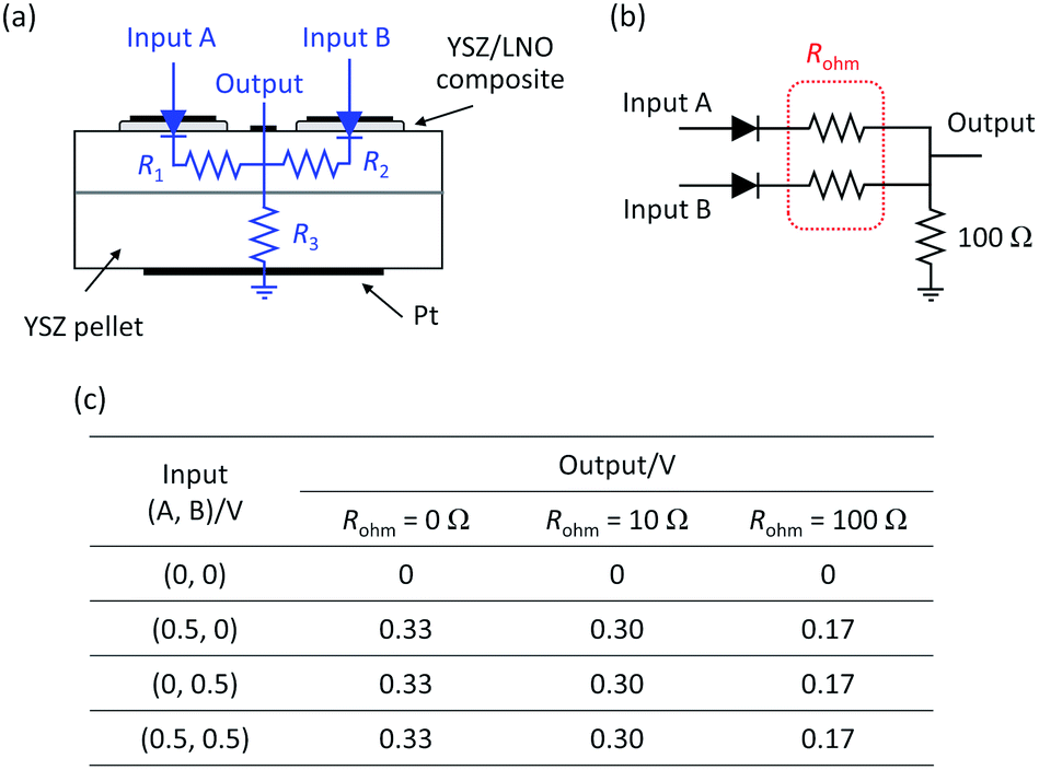 | ||
| Fig. 6 (a) Schematic picture of the ionic OR gate composed of the YSZ/LNO heterojunction and corresponding equivalent circuit. (b) The model OR gate used in the circuit response simulation. Rohm represents the ohmic resistance along the lateral direction of the substrate. (c) Electric responses of the model OR gate with different Rohm. | ||
The stability of the high temperature ionic AND and OR circuits were examined by switching the applied voltage. Proper electric responses were observed after 60 h operations and 60 times bias switching of (0, 0), (1, 0), (0, 1) and (1, 1) at 1073 K (Fig. 5d and e). No significant degradation of electric response was observed both in the ionic AND and OR gates, suggesting that high temperature ionic logic gates composed of solid–electrolyte junctions can be stably operated at high temperatures as expected.
Although we succeeded to demonstrate the high-temperature ionic logic gates composed of solid electrolyte heterojunction, the device performance was not optimized in this work. Some perspectives for further improvement are briefly summarized. Since the ionic rectification is the interfacial phenomena, the optimization of the solid electrolyte heterojunction is very important to improve the devices performance. For a bulk heterojunction, the ratio of the solid electrolytes, the particle size and its distribution, the porosity and the tortuosity are considered to be key parameters. The modification of interface structure also contributes to the speeding-up of the device response which is one of the most serious issues in this work. As mentioned above, decreasing the thickness of the solid electrolyte layer is an effective approach to make the interface responses clear and minimize the device size. Moreover, further exploration of an ionic rectifying interface is needed. A variety of combinations of solid electrolytes remain unexamined.
Conclusions
In summary, high-temperature logic gates composed of the ionic rectifying interface were successfully demonstrated in this work. The YSZ/LNO heterojunction exhibited strong ionic rectification at 1073 K (rectification ratio: 23.2 @ ± 2 V), owing to the perturbation of oxygen chemical potential at the heterojunction and electrolytic oxygen evolution and incorporation reaction. Stable operation at 1073 K of the high-temperature ionic AND and OR gates composed of the YSZ/LNO heterojunction was verified. Despite the relatively weak logic response and slow responsiveness, the present work is a promising preliminary demonstration of an ultra-high temperature logic gate utilizing a solid electrolyte diode composed of ceramic-based oxide ion conductors.Author contributions
Takashi Nakamura: conceptualization, funding acquisition, project administration, supervision, data curation, investigation, writing – original draft, writing – review & editing. Miri Honda: investigation, methodology, data curation. Yuta Kimura: investigation and data curation. Koji Amezawa: conceptualization and supervision.Conflicts of interest
There are no conflicts to declare.Acknowledgements
This work was financially supported by JSPS KAKNHI Grant number 20K21068, TEPCO Memorial Foundation, Asahi Glass Foundation and the Research Program for CORE lab of “Dynamic Alliance for Open Innovation Bridging Human, Environment and Materials” in “Network Joint Research Center for Materials and Devices”.References
- C. Chen, Y. Zuo, W. Ye, X. Li, Z. Deng and S. P. Ong, Adv. Energy Mater., 2020, 10, 1903242 CrossRef CAS.
- L. Himanen, A. Geurts, A. S. Foster and P. Rinke, Adv. Sci., 2019, 6, 1900808 CrossRef PubMed.
- A. V. Adedeji, A. C. Ahyi, J. R. Williams, S. E. Mohney and J. D. Scofield, Solid-State Electron., 2010, 54, 736–740 CrossRef CAS.
- M. Kaneko and T. Kimoto, IEEE Electron Device Lett., 2019, 40, 866–869 Search PubMed.
- S. Muhtadi, S. Hwang, A. Coleman, F. Asif, A. Lunev, M. V. S. Chandrashekhar and A. Khan, Appl. Phys. Lett., 2017, 110, 193501 CrossRef.
- K. Kumakura and T. Makimoto, Appl. Phys. Lett., 2009, 94, 103502 CrossRef.
- M. Saremi, R. Hathwar, M. Dutta, F. A. M. Koeck, R. J. Nemanich, S. Chowdhury and S. M. Goodnick, Appl. Phys. Lett., 2017, 111, 043507 CrossRef.
- N. R. Taylor, Y. Yu, M. Ji, T. Aytug, S. Mahurin, R. Mayes, S. Cetiner, M. P. Paranthaman, D. Ezell, L. R. Cao and P. C. Joshi, Appl. Phys. Lett., 2020, 116, 252108 CrossRef CAS.
- B. Lovreček, A. Despić and J. O. M. Bockris, J. Phys. Chem., 1959, 63, 750–751 CrossRef.
- J. H. Han, K. B. Kim, H. C. Kim and T. D. Chung, Angew. Chem., Int. Ed., 2009, 48, 3830–3833 CrossRef CAS PubMed.
- K. Tybrandt, R. Forchheimer and M. Berggren, Nat. Commun., 2012, 3, 871–876 CrossRef PubMed.
- S. H. Han, S. R. Kwon, S. Baek and T. D. Chung, Sci. Rep., 2017, 7, 14068 CrossRef PubMed.
- R. Zhao, X. Zhang, J. Xu, Y. Yang and G. He, RSC Adv., 2013, 3, 23178–23183 RSC.
- D. İpekçi, E. Altıok, S. Bunani, K. Yoshizuka, S. Nishihama, M. Arda and N. Kabay, Desalination, 2018, 448, 69–75 CrossRef.
- A. Merkel, A. M. Ashrafi and J. Ečer, J. Membr. Sci., 2018, 555, 185–196 CrossRef CAS.
- M. D. Eisaman, L. Alvarado, D. Larner, P. Wang, B. Garg and K. A. Littau, Energy Environ. Sci., 2011, 4, 1319–1328 RSC.
- J. Luo, D. A. Vermaas, D. Bi, A. Hagfeldt, W. A. Smith and M. Grätzel, Adv. Energy Mater., 2016, 6, 1600100 CrossRef.
- D. M. Weekes, D. A. Salvatore, A. Reyes, A. Huang and C. P. Berlinguette, Acc. Chem. Res., 2018, 51, 910–918 CrossRef CAS PubMed.
- Y. Zhao, S. Dai, Y. Chu, X. Wu and J. Huang, Chem. Commun., 2018, 54, 8186–8189 RSC.
- H. Xie, K. Du, G. Hu, J. Duan, Z. Peng, Z. Zhang and Y. Cao, J. Mater. Chem. A, 2015, 3, 20236–20243 RSC.
- B. Cao, L. A. Adutwum, A. O. Oliynyk, E. J. Luber, B. C. Olsen, A. Mar and J. M. Buriak, ACS Nano, 2018, 12, 7434–7444 CrossRef CAS PubMed.
- R. Z. D. Fernandes, S. Aleonard, J. Ilali, A. Hammou and M. Kleitz, Solid State Ionics, 1989, 34, 253–256 CrossRef CAS.
- M. Nagata, H. Orihara and H. Iwahara, Ext. Abstr. 19th Solid State Ionics Japan, 1994, pp. 141–142 Search PubMed.
- T. Shimura, G. Egusa, H. Iwahara, K. Katahira and K. Yamamoto, Solid State Ionics, 1997, 97, 477–482 CrossRef CAS.
- G. T. Kim, S. Wang, A. J. Jacobson, Z. Yuan and C. Chen, J. Mater. Chem., 2007, 17, 1316–1320 RSC.
- A. Wadsworth, Z. Hamid, J. Kosco, N. Gasparini and I. McCulloch, Adv. Mater., 2020, 32, 2001763 CrossRef CAS PubMed.
- J. Janek, Solid State Ionics, 2000, 131, 129–142 CrossRef CAS.
- H. Schmalzried, Prog. Solid State Chem., 1992, 172, 87–97 CAS.
- H. Schmalzried, Chemical Kinetics of Solids, 2007 Search PubMed.
- Electronic circuit simulator, https://www.falstad.com/circuit/ Search PubMed.
| This journal is © The Royal Society of Chemistry 2022 |