
 Open Access Article
 This Open Access Article is licensed under a Creative Commons Attribution-Non Commercial 3.0 Unported Licence
Structural, elastic and optoelectronic properties of inorganic cubic FrBX3 (B = Ge, Sn; X = Cl, Br, I) perovskite: the density functional theory approach†
Nazmul Hasan a,
Md Arifuzzaman*b and
Alamgir Kabir*c
a,
Md Arifuzzaman*b and
Alamgir Kabir*c
aDepartment of Electrical and Computer Engineering, North South University, Dhaka 1229, Bangladesh
bDepartment of Mathematics and Physics, North South University, Dhaka 1229, Bangladesh. E-mail: md.arifuzzaman01@northsouth.edu
cDepartment of Physics, Dhaka University, Dhaka 1000, Bangladesh. E-mail: alamgir.kabir@du.ac.bd
First published on 10th March 2022
Abstract
Inorganic metal-halide cubic perovskite semiconductors have become more popular in industrial applications of photovoltaic and optoelectronic devices. Among various perovskites, lead-free materials are currently most explored due to their non-toxic effect on the environment. In this study, the structural, electronic, optical, and mechanical properties of lead-free cubic perovskite materials FrBX3 (B = Ge, Sn; X = Cl, Br, I) are investigated through first-principles density-functional theory (DFT) calculations. These materials are found to exhibit semiconducting behavior with direct bandgap energy and mechanical phase stability. The observed variation in the bandgap is explained based on the substitutions of cations and anions sitting over B and X-sites of the FrBX3 compounds. The high absorption coefficient, low reflectivity, and high optical conductivity make these materials suitable for photovoltaic and other optoelectronic device applications. It is observed that the material containing Ge (germanium) in the B-site has higher optical absorption and conductivity than Sn containing materials. A systematic analysis of the electronic, optical, and mechanical properties suggests that among all the perovskite materials, FrGeI3 would be a potential candidate for optoelectronic applications. The radioactive element Fr-containing perovskite FrGeI3 may have applications in nuclear medicine and diagnosis such as X-ray imaging technology.
1. Introduction
Metal-halide cubic perovskites are a class of semiconductors represented by the chemical formula ABX3 (where A is a cation, B is a divalent metal ion, and X is a halogen anion). Recently, they have gained enormous interest from the scientific community because of their high-efficiency solar cell applications compared to silicon-based technology.1–6 Moreover, they are found to display remarkable optoelectronic properties, such as tunable direct bandgap, long charge diffusion length, good charge carrier mobility, low carrier recombination rate, small excitation binding energy, high optical absorption, and high dielectric constant, which make them more competent in various device applications including light-emitting diodes (LEDs), photovoltaic, and solar to fuel energy conversion systems and solar cells.7–10 It is reported that the hybrid perovskite has been demonstrated a remarkable improvement over the photoconductor-based X-ray detector,11–13 spectroscopy,14 acoustic wave signal processing, and image storage devices.15 A profound understanding of the characteristics of this class of exciting materials is required to forecast their specific device applications. As a result, it is indispensable to explore the structural, mechanical and optoelectronic properties and overall features of different perovskites.Lead halide perovskites with the cubic structure have sparked immense attention because of their potential use in solid-state solar-cell systems with high power conversion competencies and relatively inexpensive and straightforward processing.16–20 Although most of the naked optoelectronic features of these materials have already proven them as potential candidates in optoelectronic technologies with the electronic, optical and maximum throughput, their toxicity issue bares them to be commercially successful. Moreover, lead-based metal halide perovskite materials dissolve to PbI2 in the presence of oxygen in the atmosphere at ambient conditions, which is environmentally detrimental.21–23 Thus, one of the major drawbacks of lead halide cubic perovskites include the instability of devices and J–V hysteresis.24 One major challenge to commercialize the perovskite solar cell is to make lead-free non-toxic halide perovskite.
There are studies to demonstrate the methods in forming thin films with cesium (Cs) at A-site, projecting the significant enhancement in efficiency for the fully inorganic lead halide perovskites by utilizing a mixed halide composition in CsPbI3 material.4 The structural, optoelectronic and vibrational properties of CsPbCl3 are investigated by Padmavathy, R. et al.6 and found that the materials are wide-band-gap semiconductors as well as dynamically unstable. Another study performed by Padmavathy, R. et al. investigated the properties for lead-free CsSnIy−yCly perovskites. They demonstrated the band gap tunability by pressure variation along with material's phase transition which was projected for UV light applications.7 Roknuzzaman et al. performed a thorough DFT investigation of a series of metal halide perovskite materials (CsBX3 (B = Ge, Sn, and X = Cl, Br, I) and CsPbX3 (X = Cl, Br, I)) employing the first-principle study.25 They investigated the structural, electro-optical, and elastic properties of Ge-based CsGeI3 materials and recommended them as the best class of perovskites after lead-free metal-halide perovskites for solar cell and optoelectronic applications. Jellicoe et al. conducted the experimental investigations on the absorption profile and photoluminescence of CsSnX3 (X = I, Br, Cl) and performed the theoretical calculations on their optical characteristics.26 Recent advancements of lead-free metal halide perovskites for photovoltaic applications as well as modulation in energy band gaps along with optoelectronic and elastic properties following different mechanisms (i.e., meal doping in B-site, hetero-valent substitution, pressure induce method) have been reported in the literature.27–36
However, no investigations are found yet in the literature on the lead-free perovskite compounds with considering Fr in the A-site for such ABX3 series where (B = Ge, Sn; X = Cl, Br, I) due to its low natural abundance. FrBX3 (B = Ge, Sn; X = Cl, Br, I) perovskite may be a gateway to understand the behavior of perovskite containing heavy radioactive element in A-site. Hence, herein we perform the first-principle calculations to study the structural, elastic, optical and enteronic properties of inorganic lead-free metal-halide perovskites FrBX3 through the Density Functional Theory (DFT) approach.
2. Computational methodology
To uncover the structural and optoelectronic properties of FrBX3 (B = Ge, Sn; X = Cl, Br, I), we perform the Density Functional Theory (DFT) simulations based on the plane-wave pseudopotential using the Cambridge Serial Total Energy Package (CASTEP) code of Materials Studio-7.0 and the structural relaxation were re-confirmed by the Vienna ab initio Simulation Package (VASP).37–42 The constructed unit cells of FrBX3 in the cubic form are shown in Fig. 1, based on which further investigations in this study are carried on. The geometry optimizations are performed by employing the Generalized Gradient Approximation (GGA) for exchange–correlation interactions into the Perdew–Burke–Ernzerhof (PBE)43,44 functional. The electron–ion interactions have been studied using the Vanderbilt's Ultrasoft pseudopotential (USP)45 with the Koelling–Harmon relativistic treatment. The Broyden–Fletcher–Goldfarb–Shanno (BFGS) algorithm46 is used to secure the optimized crystal phase to cut down the total electronic energy, internal forces, and stresses. In these calculations, the wave function is prolonged up to 450 eV as the cutoff energy for the plane wave function. A Monkhorst–Pack's K-point mesh of 10 × 10 × 10 K-points sampling in the Brillouin zone is used to secure the better convergence.42 Elastic stiffness constants (Cij) were calculated by assuming the finite strain theory within the CASTEP code.40,47 The Voigt–Reuss–Hill (VRH) averaging scheme48 along with the relevant equations28,49 are used to calculate the polycrystalline mechanical parameters by setting the maximum strain amplitude to 0.003. The optical properties are calculated and analyzed excepting the scissor operator regarding an obvious depiction using the CASTEP based DFT Kohn–Sham orbitals, and supported formulae are available in the literature.50 In the present study, the optimization threshold for the geometry of the unit cells and atomic relaxation were set up in the CASTEP as follows: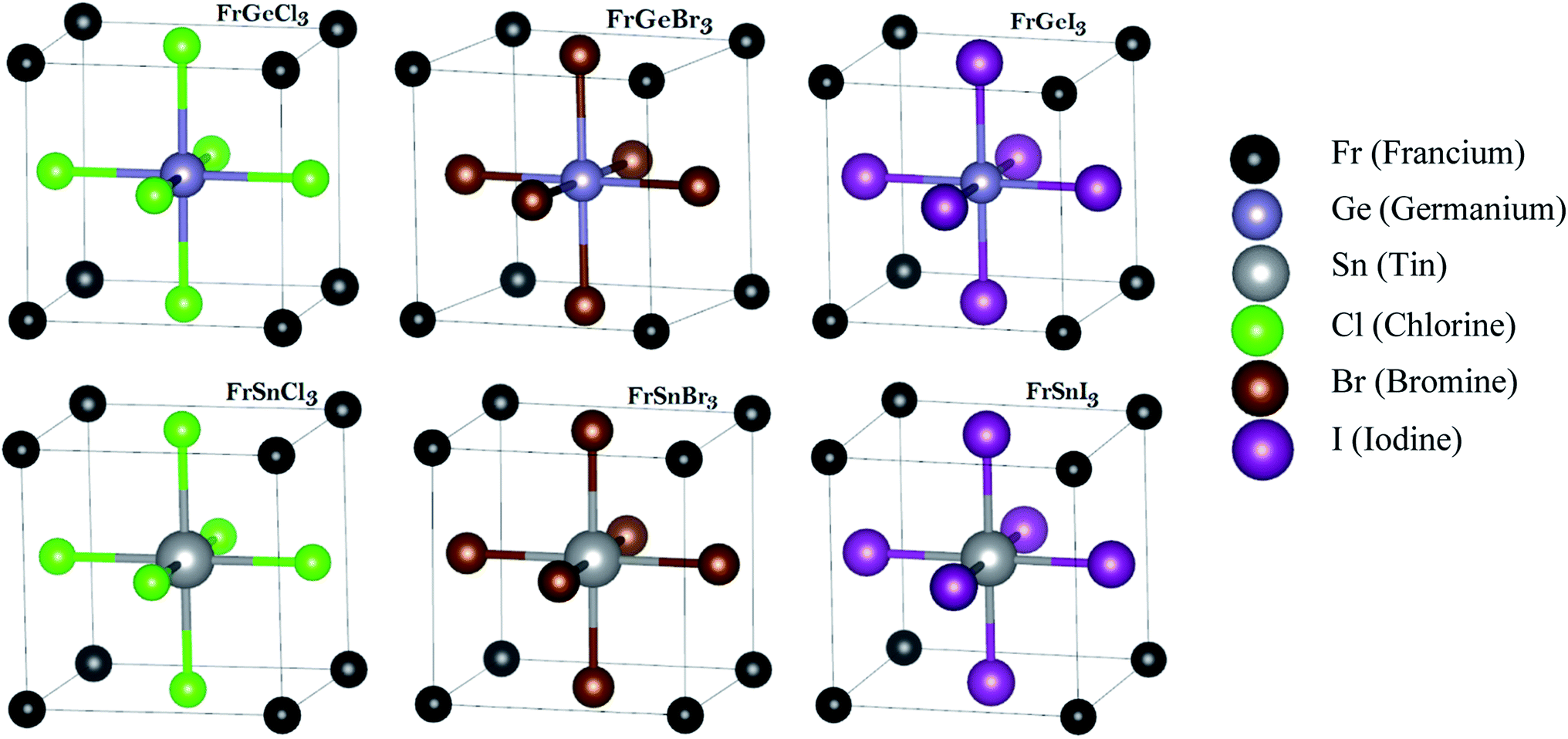 | ||
Fig. 1 The considered cubic metal halide perovskites' unit cells of FrBX3 (B ![[thin space (1/6-em)]](https://www.rsc.org/images/entities/char_2009.gif) = Ge, Sn; X = Cl, Br, I) followed by ABX3 structure. The structures are optimized within the DFT approximation. = Ge, Sn; X = Cl, Br, I) followed by ABX3 structure. The structures are optimized within the DFT approximation. | ||
• total energy 5 × 10⁻⁶ eV per atom;
• maximum force 0.01 eV per Å;
• maximum stress 0.02 GPa;
• maximum displacements 5 × 10⁻⁴ Å.
3. Results and discussion
3.1. Structural properties
The investigated materials FrBX3 (B = Ge, Sn; X = Cl, Br, I) belong to the cubic crystal structure under the space group of Pm![[3 with combining macron]](https://www.rsc.org/images/entities/char_0033_0304.gif) m (no. 221). These crystal structures have been modeled with the program of 3D Visualization for Electronic and Structural Analysis (VESTA). The unit cell of each material comprises five atoms, as depicted in Fig. 1, where the Fr atoms occupy the corner positions of the cubes at 1-a Wyckoff coordinates of (0, 0, 0). The B-site cations are located at the 1-b Wyckoff site (0.5, 0.5, 0.5) in the crystal's body-centered positions, whereas halogen (X) atoms occupy the face-centered positions at the 3-c Wyckoff site (0, 0.5, 0.5).
m (no. 221). These crystal structures have been modeled with the program of 3D Visualization for Electronic and Structural Analysis (VESTA). The unit cell of each material comprises five atoms, as depicted in Fig. 1, where the Fr atoms occupy the corner positions of the cubes at 1-a Wyckoff coordinates of (0, 0, 0). The B-site cations are located at the 1-b Wyckoff site (0.5, 0.5, 0.5) in the crystal's body-centered positions, whereas halogen (X) atoms occupy the face-centered positions at the 3-c Wyckoff site (0, 0.5, 0.5).
The estimated lattice parameter and volumes of the optimized cells are listed in Table 1. The lattice parameter and unit cell volume are reduced when halogen atom (X) is replaced with another halogen atom of smaller ionic radius, whereas replacing germanium (Ge) by tin (Sn) in the B-site exhibits the opposite trend, as appeared in Table 1. With the change of halides size, a clean periodic pattern is observed in the variation of lattice parameters due to the ‘octahedral effect’ in the cell volume, which upholds the universal trend of variation in atomic size and charge of the most perovskite materials.24,51,52 Same periodical manners are also exhibited in the case of interatomic bond lengths of the materials as appeared in Table 1. The substitution of one type of atom for another in the compound affects its structural characteristics and the material's performances, such as electrical, optical, and mechanical capabilities.
| FrGeCl3 | FrGeBr3 | FrGeI3 | FrSnCl3 | FrSnBr3 | FrSnI3 | |
|---|---|---|---|---|---|---|
| a (Å) | 5.37 | 5.63 | 6.01 | 5.64 | 5.90 | 6.27 |
| V (Å3) | 154.72 | 178.42 | 217.45 | 179.83 | 205.82 | 246.30 |
| Inter atomic bond length (Å) | Fr–Ge: 4.65 | Fr–Ge: 4.87 | Fr–Ge: 5.21 | Fr–Sn: 4.88 | Fr–Sn: 5.11 | Fr–Sn: 5.43 |
| Cl–Ge: 2.68 | Br–Ge: 2.81 | I–Ge: 3.01 | Cl–Sn: 2.82 | Br–Sn: 2.95 | I–Sn: 3.13 | |
| Fr–Fr: 5.37 | Fr–Fr: 5.63 | Fr–Fr: 6.01 | Fr–Fr: 5.64 | Fr–Fr: 5.90 | Fr–Fr: 6.27 | |
| Cl–Cl: 3.79 | Br–Br: 3.98 | I–I: 4.25 | Cl–Cl: 3.99 | Br–Br: 4.17 | I–I: 4.43 | |
| Inter atomic bond angles (°) | Fr–Ge–Cl: 54.74 | Fr–Ge–Br: 54.74 | Fr–Ge–I: 54.74 | Fr–Sn–Cl: 54.74 | Fr–Sn–Br: 54.74 | Fr–Sn–I: 54.74 |
| Cl–Ge–Cl: 90 | Br–Ge–Br: 90 | I–Ge–I: 90 | Cl–Sn–Cl: 90 | Br–Sn–Br: 90 | I–Sn–I: 90 |
As different cations can be incorporated into the ABX3 cubic perovskite framework resulting in the development of diverse materials with identical properties, so the tolerance factor has a significance to discovery of alternative lead-halide perovskites. Concerning with perovskite materials' efficiency with solar conversion, instability in phase in ambient environment and rapid crystallization during the fabrication process are highly effect. Following the no-rattling principle for the perovskites, the perovskite forming factor by geometric conditions empowers us to anticipate perovskites with an 80% fidelity. The tolerance factors for the investigated perovskite materials are calculated using the Goldschmidt's tolerance factor following the equation: T = (RA + RX)/√2 (RB + RX), where RA, RB, RX stands for the ionic radii for A, B, and X site ions respectively. It is observed from the Table 2 that the tolerance factor is varied in range of 0.84 to 1.00 in which Ge based materials' values exhibit close to 1 to strongly recommend that the formation of an ideal and tightly packed stable cubic perovskite structure having size of cation A larger than that of B.53,54
| Element | T | IFF | RA | RB | RX |
|---|---|---|---|---|---|
| FrGeCl3 | 1.00 | 0.65 | Ge2+ 0.73 Å | Cl− 1.81 Å | |
| FrGeBr3 | 0.99 | 0.68 | |||
| FrGeI3 | 0.96 | 0.74 | Fr+ 1.80 Å | Br− 1.96 Å | |
| FrSnCl3 | 0.85 | 0.58 | |||
| FrSnBr3 | 0.85 | 0.61 | Sn2+ 1.10 Å | I− 2.20 Å | |
| FrSnI3 | 0.84 | 0.66 |
3.2. Electronic properties
The electronic properties are primarily analyzed considering the high symmetry directions of the Brillouin zone. The electronic band structures and density of states (DOS) of the pristine FrBX3 (B = Ge, Sn; X = Br, Cl, I) compounds have been calculated through the PBE functional assuming the GGA approximation. The band structure of the FrBX3 is shown in Fig. 2. The energy band is considered from −5 eV to +5 eV in this study, and zero-point energy is taken as Fermi energy. It is clear from Fig. 2 that all six structures exhibit the direct bandgap. The value of the bandgaps is reported in Table 3. The range of the bandgap energy indicates that the structures are semiconductor in nature. The valence band and bottom of the conduction band of all structures are located in the high symmetry R points in the Brillouin zone, which confirm the direct bandgap semiconducting nature of the FrBX3 perovskite material. The retrieved bandgaps and band structures of the investigated materials suggest their novelty for photothermal, photovoltaic, and other optoelectronic applications. According to the semi-conductive theory, the nature of the materials can be confirmed precisely through their band structure patterns with reference to the Fermi level. Table 3 presents the calculated electronic band gap values for the compounds in this study, which are the characteristics of other perovskite materials containing ABX3 structure as found in the literature.7,15,20–24,27–30 The present study is focused on observing the variation in bandgap due to the substitution of cations and anions over B- and X-sites of the FrBX3 compounds.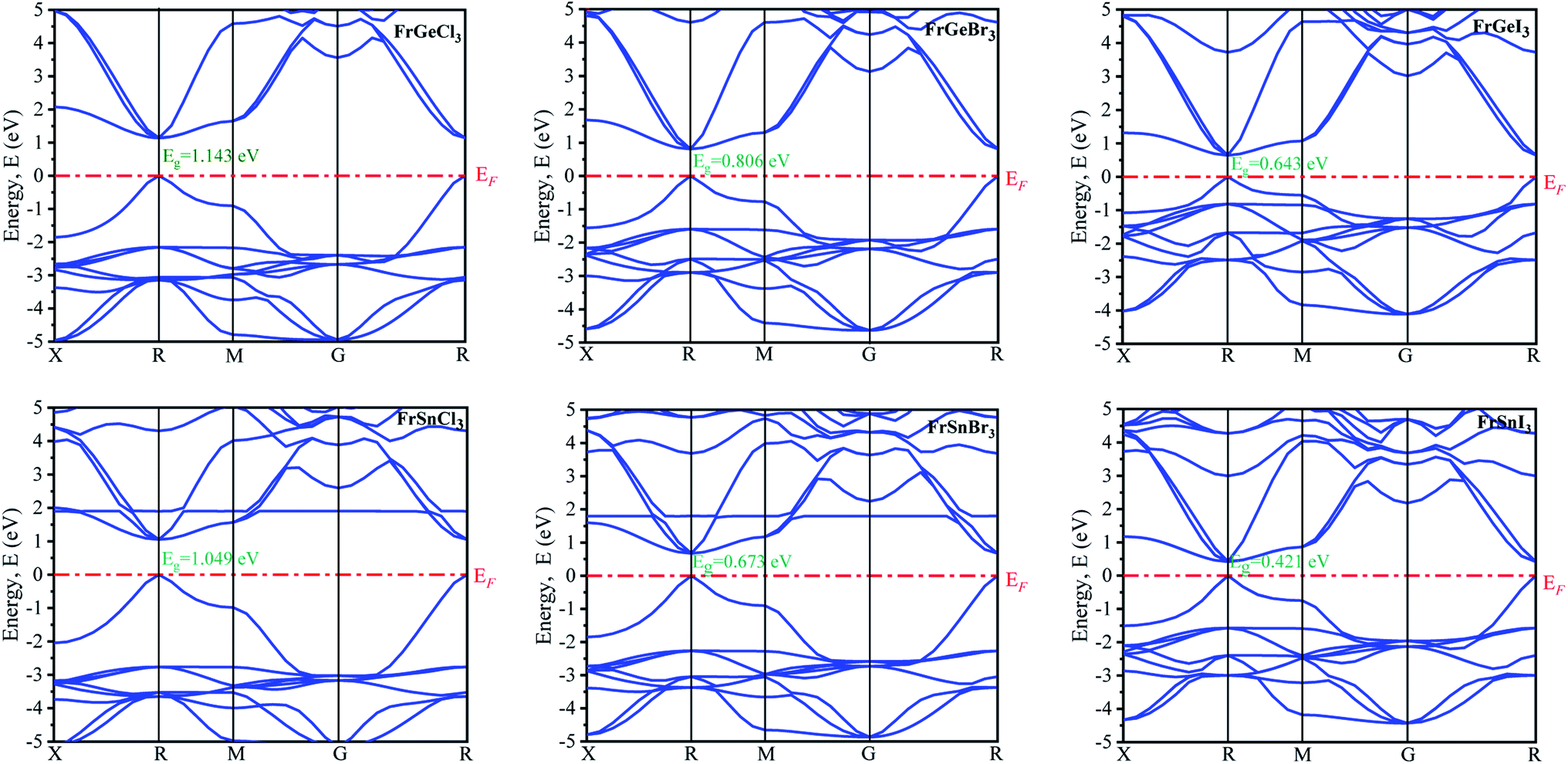 | ||
| Fig. 2 Electronic band structures of FrBX3 (B = Ge, Sn; X = I, Br, Cl). | ||
| Samples | Electronic bandgap, Eg (eV) |
|---|---|
| FrGeCl3 | 1.14 eV |
| FrGeBr3 | 0.81 eV |
| FrGeI3 | 0.64 eV |
| FrSnCl3 | 1.05 eV |
| FrSnBr3 | 0.67 eV |
| FrSnI3 | 0.42 eV |
The variation of energy bandgap with respect to the change of halogen in the X site are shown in Fig. 2. The electronic band gap energy value decreases as we replaced Ge by Sn on B site for the same halogen atom, with a slight shift of conduction band towards the Fermi level in the band structures as observed in Fig. 2. This decrease in the bandgap may be attributed to the increase of cell parameters for the FrSnX3 compound as compared to the FrGeX3 compound. As we change the halogen atom in X site for the FrGeX3 element, a decrease in bandgap with larger halogen atoms is observed as in the Fig. 3. The trend is similar for the FrSnX3 compound. The interatomic distance will aggrandize as the lattice constant increases. As a result, the valence electrons' binding forces will weaken which will be lied in the valence band. However, bounding valence electrons require energy to move freely within the material and become conduction electrons and the energy gap is the minimum energy required to convert valence electrons to conduction electrons. As the interatomic distance increases, the valence electrons become less bound, requiring less energy to free them in the conduction band. However, the compositional dependence of the lattice constant for lattice mismatch at the interfaces of heterostructures, as well as the periodic potential field of the material, play an important role on the wave function of the valence electrons in a semiconductor crystal, which leads to variation in the energy band gap.55 Furthermore, the energy gap is inversely proportional to the dielectric constant, which is inversely proportional to the inter-atomic distance. Consequently, increasing the lattice constant results in the decrease of the electronic band gap.
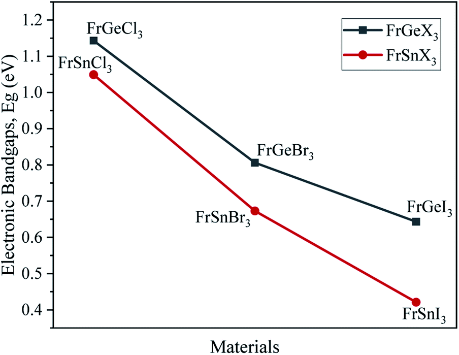 | ||
| Fig. 3 Variations of the electronic bandgap due to the effect of B- and X-site substitutions. | ||
The tunability of band structures and observed bandgaps due to the change of atoms over B- and X-sites in metal halide cubic perovskite materials have made them prominent for various photovoltaic applications.
The calculated atom projected density of states are presented in Fig. 4(A)–(F). The total density of states (TDOS) and orbital projected density of states (PDOS) of each materials and constituted elements are available in ESI Fig. (S2–S8†) for the pristine FrBX3. From Fig. 4, it is clear that the halogen atoms contribute more on the bottom of the conduction band, and the metal on the B-site (Ge or Sn) contributes more on top of the valence band. The Fermi level is situated adjacent to the top of the valence band. The orbital projected DOS (ESI Fig. S3–S8†) revealed that at the Fermi level, the main contribution comes from the p-orbital of the halogen atom and the valence band maxima composed of the p-orbital of the Fr atom. The replacement of atoms in B site by Sn results in the slight increase of electronic states in the valence bands (VBs) below the (EF) Fermi level. However, the change in halogen atoms leads to demonstrate opposite trends in electronic states. The investigated systems' conduction bands (CBs) result from halogens' and B-site atoms' p orbital, and the Fr atom contribute very less at the Fermi level. The significant contribution comes mainly from the Fr atom in the deep energy level between −8 eV and −6 eV. No hybridization in the generation of energy levels in the Fermi level is noticed for all configurations.
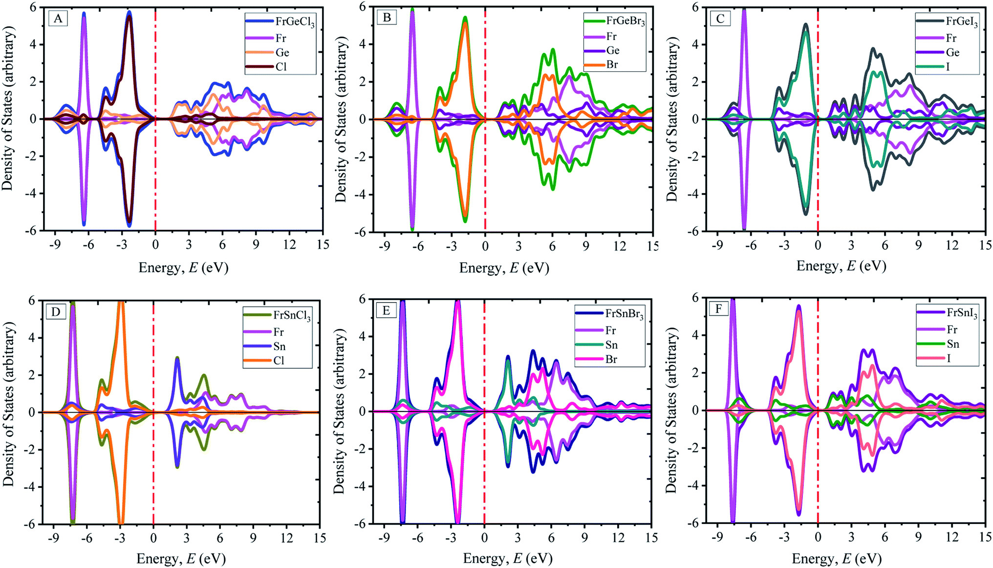 | ||
| Fig. 4 Atom projected electronic density of states (DOS) of perovskites FrBX3 (B = Ge, Sn; X = I, Br, Cl). | ||
3.3. Optical properties
A material's optical characteristics are the most fundamental parameters for its competence in optoelectronic and photovoltaic applications since they provide essential information about its interaction with light. Optical functions of a material are essential to the better understanding of the materials' electronic configuration and determine their suitability in photovoltaic applications. Therefore, the detailed optical properties of the considered cubic perovskite materials, such as absorption spectra with respect to the light energy and wavelength, reflectivity, refractive index, dielectric constants, and optical conductivity, are examined up to 30 eV of photon energy.The optical absorption coefficient (α) indicates how much light of particular photon energy or wavelength penetrates the substance before being absorbed by the material. That provides vital knowledge on the material's optimum solar-energy conversion efficiency for practical applications. In Fig. 5, the evaluated photon energy-dependent (Fig. 5(A) and (C)) and wavelength-dependent (Fig. 5(B) and (D)) absorption profiles of the considered pure compounds are demonstrated. Generally, three significant peaks are observed for the compounds, as shown in Fig. 5(A) for the FrGeX3 compound, where a small peak at 6 eV photon energy is observed. The small peak at 6 eV photon energy becomes prominent for the case of the FrSnX3 compound as shown in Fig. 5(C). Changing in B site by Sn also results in the amplitude of the absorption spectra decreasing, keeping the peaks position at the same energy level. The highest peaks for the all-pristine compounds are found at ∼14 eV, whereas the second highest peak is found at ∼9 eV for FrGeX3 compounds, and a slight change towards the low energy region (<10 eV) is observed for FrSnX3. However, the highest peaks are found for Cl-containing materials at the halogen site at ∼14 eV as observed from the absorption profiles in Fig. 5(A) and (C). The first peak for all compounds is observed from 2.5 eV to 5 eV in the low-energy region, which is much larger than the value of bandgap as reported in the Fig. 2. This is due to the underestimation of bandgap of the LDA exchange correlation potential. Changes in halide atoms affect the absorption magnitudes; I-containing materials (FrB [= Ge, Sn]I3) exhibit more absorption at low energy regions and a wider absorption profile compared to Br- and Cl-containing compounds. The higher absorption in the low-energy region indicates the material to be a probable candidate for the solar cell application since the sun radiates more energy in the visible region. The absorption profiles with respect to the wavelength are exhibited in Fig. 5(B) and (D) that are projected to further understand the light absorbance behavior of the particular FrBX3 series compounds in the visible range of the light spectrum. According to Fig. 5(B) and (D), I-containing materials demonstrate a comparatively higher peak in the visible region with a wider absorption region than Br- and Cl-containing materials. Besides, with the substitution of Ge by Sn in the B-site, there is a drastic decrease in absorption peak as depicted in Fig. 5. The extracted results for the Fr-based series are in line with the results found in literature for such ABX3 lead-free perovskite materials.24,25,28,32–34,36,56 Generally, approximately 43% of the solar spectrum is covered by visible light, whereas only 4% of solar energy contribution comes from the ultraviolet light. Therefore, to take advantage of the visible light energy solar spectrum for photovoltaic conversion, intrinsic FrGeX3 exhibits more suitability than FrSnX3 from the application point of view.
 | ||
| Fig. 5 Absorption spectra of FrBX3 (B = Ge, Sn; X = I, Br, Cl) as a function of wavelength and photon energy. | ||
Reflectivity is an optical property of materials to understand the surface nature of perovskites. The reflectivity determines how much light energy is reflected from the materials' surface compared to the light-energy incident on the surface. The reflectivity spectra of pristine FrBX3 compounds are illustrated in Fig. 6(A) for FrGeX3 and 6(B) for FrSnX3 compound, for photon energy up to 30 eV. From Fig. 6(A) and (B), it is observed that all the materials exhibit identical behavior with providing low reflectivity in the whole spectrum. Exceptionally, Cl-containing materials show an additional peak in the UV region, indicating the significant absorptivity and/or transmission. At the low energy region, FrBI3 (B = Ge, Sn) materials reflect more energy compared to the other compound and the maximum reflectivity of 0.38 is observed for FrGeI3. This moderate reflectivity at the visible region indicates the material to be a good candidate for solar cell applications. The dielectric variation of the investigated perovskite materials is illustrated in Fig. 7(A), for up to 30 eV photon energy. The detected patterns indicate that the materials are highly transmittable in the high energy region as well as low transmittance in the low energy region. The dielectric constant values are used to determine how well optoelectronic devices work, defined as a material's response to incident light energy. The greater dielectric values at a lower charge carrier recombination rate are profound in improving the optoelectronic device performance in the long run. From both real and imaginary dielectrics, it is evident that materials comprising with I exhibit comparatively higher amplitude of dielectric constant than other samples in the visible region. Light propagation behavior in absorbing materials can be portrayed with the refractive index value. The greater the refractive index, the closer the light will travel to its normal direction. The refractive index of all studied perovskites is qualitatively similar, with a little variation in peak heights and placements as displayed in ESI Fig. S9.† The static refractive index varies depending on the compound n(0), which is found a maximum of 3.15 for FrGeI3, and the minimum value of 2.25 is found for FrSnCl3. Besides, optically conductive materials also ascertain the photoconductivity, which increases electric conductivity with the rise of both photon absorption of electromagnetic radiation. The variations in optical conductivity for the pristine FrBX3 compounds are shown in Fig. 7(E) and (F). At low energies, it is clear that the majority of the compounds have a noticeable optical conductivity. The highest amplitudes are depicted for Cl-containing materials in the high-energy region, while I-containing compounds exhibit the opposite manner. However, Ge-containing materials exhibit higher conductivity compared to Sn-based samples, which confirms the better performance of FrGeX3.
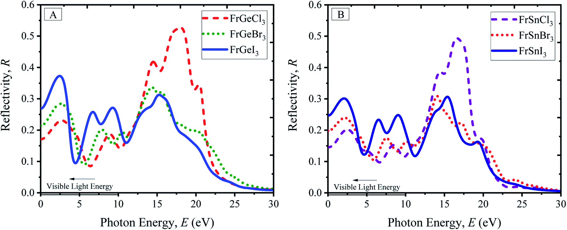 | ||
| Fig. 6 Reflectivity profile of perovskites (A) FrGeX3 (X = I, Br, Cl), and (B) FrSnX3 (X = I, Br, Cl). | ||
 | ||
| Fig. 7 Real and imaginary part of the dielectric constant for FrGeX3 are presented in (A) and (B) respectively, and for FrSnX3, presented in (C) and (D). The optical conductivity of FrGeX3 with respect to the photon energy is presented in (E) and that of FrSnX3 in (F). | ||
3.4. Mechanical properties
The elastic constants depict a clear understanding of the mechanical stability in any crystals. This study employed the CASTEP module to calculate the elastic constants using finite strain theory. The three independent elastic constants for the cubic perovskites C11, C12, and C44 are evaluated using the CASTEP stress–strain method and listed in Table 4. As for the cubic symmetry, the Born-stability criterion as follows, C11 > 0, C44 > 0, C11–C12 > 0, and C11 + 2C12 > 0, should be met by perovskite materials. It is evident from Table 3 that these pristine FrBX3 perovskite compounds agree well to bear this study's reliability. Observation of the Cauchy pressure (C12–C44) is an essential and valuable parameter for predicting the compounds' brittleness and ductility. From the retrieved values of Cauchy pressure, it is observed that all the pristine materials exhibiting positive values correspond to the ductile nature except for FrGeI3 giving negative values. Hill approximations are used to estimate the most crucial mechanical parameters for the polycrystalline materials, such as bulk modulus B and shear modulus G using the single-crystal elastic constants. However, Young's modulus Y, Pugh's ratio B/G, and the Poisson's ratio v of these pristine compounds are determined using the following formula,
| Phase | C11 | C12 | C44 | C12–C44 | B (GPa) | G (GPa) | Y (GPa) | B/G | v |
|---|---|---|---|---|---|---|---|---|---|
| FrGeCl3 | 52.41 | 13.69 | 12.17 | 1.52 | 26.60 | 14.67 | 37.18 | 1.81 | 0.27 |
| FrGeBr3 | 45.86 | 10.89 | 10.28 | 0.61 | 22.55 | 12.73 | 32.14 | 1.77 | 0.26 |
| FrGeI3 | 33.17 | 6.55 | 7.51 | −0.96 | 15.42 | 9.46 | 23.56 | 1.63 | 0.24 |
| FrSnCl3 | 48.41 | 9.82 | 6.54 | 3.28 | 22.68 | 10.27 | 26.77 | 2.21 | 0.30 |
| FrSnBr3 | 42.11 | 7.72 | 5.37 | 2.35 | 19.18 | 8.75 | 22.78 | 2.19 | 0.30 |
| FrSnI3 | 33.64 | 4.94 | 3.64 | 1.30 | 14.50 | 6.55 | 17.08 | 2.21 | 0.30 |
Accordingly, bulk modulus (B) is one of the noteworthy mechanical parameters that provide an insight into the material's rigidity. All the investigated materials show flexibility and softness, as observed from the calculated bulk modulus values ranging between 14.50 GPa (for FrSnI3) and 26.60 GPa (for FrGeI3). Therefore, such metal-halide perovskite materials can be easily incorporated into thin films for solar cell applications due to their flexibility and softness. The change in halide ion from Cl to I results in a decrease in bulk modulus value for all the samples; where a change in B site with Ge from Sn leads to the opposite trend slightly, and a similar tendency is seen for shear modulus (G) and young modulus (Y). Pugh's ratio (B/G) and Poisson ratio v are used to predict a material's failure mechanism, i.e., its ductility and brittleness. Pugh's ratio distinguishes ductile from brittle materials, and the Poisson ratio indicates ductile from brittle materials with a crucial value of 1.75 and 0.26, respectively. Pugh's ratio more than 1.75, or Poisson ratio greater than 0.26, indicates ductility; otherwise, it indicates brittleness. The criteria state that FrGeI3 is brittle, FrGeBr3 is at the brittle-ductile boundary, and the remaining compounds are ductile, as seen from the value in Table 4, while the Poisson ratio has the same characteristics. Hence, for the device applications, FrGeI3 would be challenging because its low Pugh's ratio and Poisson ratio indicate its' brittle nature. In contrast, compounds containing Cl have a higher degree of ductility, and FrSnCl3 has the most ductility of the bunch.
3.5. Environmentally-friendly (lead-free) perovskites
Table 5 shows an overview of the essential features of the metal halide perovskites that are studied. Ge-based compounds, in comparison, show stronger optical absorbance and photoconductivity in the low-energy region than Sn-based compounds, implying a better B site element to be germanium (Ge) with Fr in A site. Furthermore, the optical absorbance and conductivity of the Sn-based compounds, FrSnX3 (X = Cl, Br, I), are comparatively lower than those of Ge-based compounds. Henceforth, due to its strong absorption and photoconductivity throughout the solar spectrum, FrGeI3 can be considered as the potential lead-free perovskite material for photovoltaic applications if one can take care of the small brittleness nature of this compound. Contrariwise, FrGeCl3 is ductile but has a significant band gap, rendering it unsuitable for solar visible light absorption. However, by incorporating another halide ion in the X site and/or a metal in the B-site with FrGeI3 following the solid solution or doping methods as well as other methods introduced in DFT literature, film formation may be improved by reducing the brittleness of the materials.25,29–34,56–59 However, as a test calculation we have performed the solar cell device simulation using SCAPS 1D simulation software for the FrGeI3. In this simulation the absorption profile of the perovskite FrGeI3 is used which was extracted from the DFT simulation, and for HTL we have used CZTSe where TiO2 is used for ETL materials. As the contact materials, we used gold and FTO. The simulated I–V graph can be found in Fig. S10 in the ESI† with other relevant parameters. With the extracted parameters, the PCE is found to be 15.07% which is subjected to further optimizations.| Properties | Optical absorption | Photoconductivity | Failure mode |
|---|---|---|---|
| FrGeCl3 | High [UV-region] | Moderate | Ductile |
| Less [visible region] | |||
| FrGeBr3 | High [UV-region] | Moderate | Ductile |
| Medium [visible-region] | |||
| FrGeI3 | High [UV-region] | High | Brittle |
| High [visible-region] | |||
| FrSnCl3 | High [UV-region] | Less | Ductile |
| Less [visible-region] | |||
| FrSnBr3 | High [UV-region] | Moderate | Ductile |
| Medium [visible-region] | |||
| FrSnI3 | High [UV-region] | Moderate | Ductile |
| Medium [visible-region] |
4. Conclusion
FrBX3 (B = Sn, Ge; X = I, Br, Cl), a Pb-free inorganic metal-halide (MH) cubic perovskite was studied using the first-principle of DFT simulations to evaluate its structural, electrical and optical properties. A decrease of electronic band gap (Eg) is observed while using Cl, Br, I in the halogen site, respectively, and that tends to be a slight change in other properties (variations in the halogen contents in these materials can be used to modulate the bandgap). Ge appears to be a superior candidate than Sn as Ge-based compounds exhibit higher optical absorption and optical conductivity compared to that Sn-based materials. Though Fr is radioactive, the studied materials are found to be mechanically stable in nature and can be grown into thin films easily due to their low bulk modulus. Considering the retrieved structural, mechanical and optoelectronic properties, it is inferred that FrBX3 (B = Ge, Sn; X = Cl, Br, I) would be an excellent candidate as a metal-halide perovskite for various photovoltaic applications including photoconductor-based X-ray detector. According to the existing knowledge in the literature, a further study based on the doping of different cations in B- and X-sites along with the pressure-induced study may resolve the issue.Conflicts of interest
There are no conflicts to declare.Acknowledgements
The authors are grateful to the center of excellence of the Department of Mathematics and Physics, North South University (NSU), Dhaka 1229, Bangladesh. This research is funded by the NSU research grant CTRG-20/SEPS/13. The authors are grateful to Dr Mozahar Ali and Mr Sadiq Shahriyar Nishat for their useful suggestions regarding the DFT calculation.References
- L. Chouhan, S. Ghimire, C. Subrahmanyam, T. Miyasaka and V. Biju, Synthesis, optoelectronic properties and applications of halide perovskites, Chem. Soc. Rev., 2020, 49(10) 10.1039/C9CS00848A.
- W. Zhang, G. E. Eperon and H. J. Snaith, Metal halide perovskites for energy applications, Nat. Energy, 2016, 1(6) DOI:10.1038/nenergy.2016.48.
- W.-J. Yin, T. Shi and Y. Yan, Unique Properties of Halide Perovskites as Possible Origins of the Superior Solar Cell Performance, Adv. Mater., 2014, 26(27) DOI:10.1002/adma.201306281.
- R. J. Sutton, et al., Bandgap-Tunable Cesium Lead Halide Perovskites with High Thermal Stability for Efficient Solar Cells, Adv. Energy Mater., 2016, 6(8) DOI:10.1002/aenm.201502458.
- A. Kojima, K. Teshima, Y. Shirai and T. Miyasaka, Organometal Halide Perovskites as Visible-Light Sensitizers for Photovoltaic Cells, J. Am. Chem. Soc., 2009, 131(17) DOI:10.1021/ja809598r.
- R. Padmavathy, A. Amudhavalli, R. Rajeswarapalanichamy and K. Iyakutti, Electronic and Optical Properties of Cubic Perovskites CsPbCl3−yIy (y = 0, 1, 2, 3), Z. Naturforsch., 2019, 74(10) DOI:10.1515/zna-2018-0516.
- R. Padmavathy, A. Amudhavalli, M. Manikandan, R. Rajeswarapalanichamy, K. Iyakutti and A. K. Kushwaha, Electronic and Optical Properties of CsSnI3−yCly (y = 0, 1, 2, 3) Perovskites: a DFT Study, J. Electron. Mater., 2019, 48(2) DOI:10.1007/s11664-018-06850-8.
- G. E. Eperon, et al., Inorganic caesium lead iodide perovskite solar cells, J. Mater. Chem. A, 2015, 3(39) 10.1039/C5TA06398A.
- P. Ramasamy, D.-H. Lim, B. Kim, S.-H. Lee, M.-S. Lee and J.-S. Lee, All-inorganic cesium lead halide perovskite nanocrystals for photodetector applications, Chem. Commun., 2016, 52(10) 10.1039/C5CC08643D.
- J. Li, et al., Perovskite Single Crystals: Synthesis, Optoelectronic Properties, and Application, Adv. Funct. Mater., 2021, 31(11) DOI:10.1002/adfm.202008684.
- Q. Xu, et al., High-Performance Surface Barrier X-ray Detector Based on Methylammonium Lead Tribromide Single Crystals, ACS Appl. Mater. Interfaces, 2019, 11(10), 9679–9684, DOI:10.1021/acsami.8b21605.
- Y. Zhou, J. Chen, O. M. Bakr and O. F. Mohammed, Metal Halide Perovskites for X-ray Imaging Scintillators and Detectors, ACS Energy Lett., 2021, 6(2), 739–768, DOI:10.1021/acsenergylett.0c02430.
- W. Zhu, et al., Low-dose real-time X-ray imaging with nontoxic double perovskite scintillators, Light: Sci. Appl., 2020, 9(1), 112, DOI:10.1038/s41377-020-00353-0.
- L. R. Cao, L. Pan, P. Kandlakunta and W. Nie, Perovskite detectors for X-ray imaging and gamma spectroscopy: overview and current state-of-the-art, in Hard X-Ray, Gamma-Ray, and Neutron Detector Physics, 2021, vol. XXIII, p. 11, DOI:10.1117/12.2595913.
- E. A. R. Assirey, Perovskite synthesis, properties and their related biochemical and industrial application, Saudi Pharm. J., 2019, 27(6), 817–829, DOI:10.1016/j.jsps.2019.05.003.
- F. Sahli, et al., Fully textured monolithic perovskite/silicon tandem solar cells with 25.2% power conversion efficiency, Nat. Mater., 2018, 17(9) DOI:10.1038/s41563-018-0115-4.
- Y. H. Chang, C. H. Park and K. Matsuishi, First-principles study of the structural and the electronic properties of the lead-halide-based inorganic–organic perovskites (CH3NH3)PbX3 and CsPbX3 (X = Cl, Br, I), J. Korean Phys. Soc., 2004, 44(4), 889–893 CAS.
- G. Murtaza and I. Ahmad, First principle study of the structural and optoelectronic properties of cubic perovskites CsPbM3 (M = Cl, Br, I), Phys. B, 2011, 406(17) DOI:10.1016/j.physb.2011.05.028.
- M. Afsari, A. Boochani and M. Hantezadeh, Electronic, optical and elastic properties of cubic perovskite CsPbI3: using first principles study, Optik, 2016, 127(23) DOI:10.1016/j.ijleo.2016.09.013.
- M. A. Ghebouli, B. Ghebouli and M. Fatmi, First-principles calculations on structural, elastic, electronic, optical and thermal properties of CsPbCl3 perovskite, Phys. B, 2011, 406(9) DOI:10.1016/j.physb.2011.02.040.
- A. Babayigit, et al., Assessing the toxicity of Pb- and Sn-based perovskite solar cells in model organism Danio rerio, Sci. Rep., 2016, 6(1) DOI:10.1038/srep18721.
- G. E. Eperon, et al., The Importance of Moisture in Hybrid Lead Halide Perovskite Thin Film Fabrication, ACS Nano, 2015, 9(9) DOI:10.1021/acsnano.5b03626.
- A. Babayigit, A. Ethirajan, M. Muller and B. Conings, Toxicity of organometal halide perovskite solar cells, Nat. Mater., 2016, 15(3) DOI:10.1038/nmat4572.
- S. F. Hoefler, G. Trimmel and T. Rath, Progress on lead-free metal halide perovskites for photovoltaic applications: a review, Monatsh. Chem., 2017, 148(5) DOI:10.1007/s00706-017-1933-9.
- M. Roknuzzaman, K. Ostrikov, H. Wang, A. Du and T. Tesfamichael, Towards lead-free perovskite photovoltaics and optoelectronics by ab-initio simulations, Sci. Rep., 2017, 7(1) DOI:10.1038/s41598-017-13172-y.
- T. C. Jellicoe, et al., Synthesis and Optical Properties of Lead-Free Cesium Tin Halide Perovskite Nanocrystals, J. Am. Chem. Soc., 2016, 138(9) DOI:10.1021/jacs.5b13470.
- E. T. McClure, M. R. Ball, W. Windl and P. M. Woodward, Cs2 AgBiX6 (X = Br, Cl): New Visible Light Absorbing, Lead-Free Halide Perovskite Semiconductors, Chem. Mater., 2016, 28(5) DOI:10.1021/acs.chemmater.5b04231.
- J. Islam and A. K. M. A. Hossain, Narrowing band gap and enhanced visible-light absorption of metal-doped non-toxic CsSnCl3 metal halides for potential optoelectronic applications, RSC Adv., 2020, 10(13) 10.1039/C9ra10407k.
- M. Z. Rahaman and A. K. M. Akther Hossain, Effect of metal doping on the visible light absorption, electronic structure and mechanical properties of non-toxic metal halide CsGeCl3, RSC Adv., 2018, 8(58) 10.1039/C8RA06374E.
- Q. Wang, N. Phung, D. di Girolamo, P. Vivo and A. Abate, Enhancement in lifespan of halide perovskite solar cells, Energy Environ. Sci., 2019, 12(3) 10.1039/C8EE02852D.
- R. Nie, R. R. Sumukam, S. H. Reddy, M. Banavoth and S. il Seok, Lead-free perovskite solar cells enabled by hetero-valent substitutes, Energy Environ. Sci., 2020, 13(8) 10.1039/D0EE01153C.
- M. N. Islam, M. A. Hadi and J. Podder, Influence of Ni doping in a lead-halide and a lead-free halide perovskites for optoelectronic applications, AIP Adv., 2019, 9(12) DOI:10.1063/1.5132985.
- M. A. Islam, J. Islam, M. N. Islam, S. K. Sen and A. K. M. A. Hossain, Enhanced ductility and optoelectronic properties of environment-friendly CsGeCl 3 under pressure, AIP Adv., 2021, 11(4) DOI:10.1063/5.0048849.
- M. I. Kholil, M. T. H. Bhuiyan, M. A. Rahman, M. S. Ali and M. Aftabuzzaman, Effects of Fe doping on the visible light absorption and bandgap tuning of lead-free (CsSnCl3) and lead halide (CsPbCl3) perovskites for optoelectronic applications, AIP Adv., 2021, 11(3) DOI:10.1063/5.0042847.
- S. F. Hoefler, G. Trimmel and T. Rath, Progress on lead-free metal halide perovskites for photovoltaic applications: a review, Monatsh. Chem., 2017, 148(5) DOI:10.1007/s00706-017-1933-9.
- M. Román-Vázquez, C. C. Vidyasagar, B. M. Muñoz-Flores and V. M. Jiménez-Pérez, Recent advances on synthesis and applications of lead- and tin-free perovskites, J. Alloys Compd., 2020, 835 DOI:10.1016/j.jallcom.2020.155112.
- W. Kohn and L. J. Sham, Self-Consistent Equations Including Exchange and Correlation Effects, Phys. Rev. A: At., Mol., Opt. Phys., 1965, 140(4) DOI:10.1103/PhysRev.140.A1133.
- P. Hohenberg and W. Kohn, Inhomogeneous Electron Gas, Phys. Rev. B: Solid State, 1964, 136(3) DOI:10.1103/PhysRev.136.B864.
- S. J. Clark, et al., First principles methods using CASTEP, Z. Kristallogr. Cryst. Mater., 2005, 220(5–6) DOI:10.1524/zkri.220.5.567.65075.
- M. D. Segall, et al., First-principles simulation: ideas, illustrations and the CASTEP code, J. Phys.: Condens. Matter, 2002, 14(11) DOI:10.1088/0953-8984/14/11/301.
- M. C. Payne, M. P. Teter, D. C. Allan, T. A. Arias and J. D. Joannopoulos, Iterative minimization techniques for ab initio total-energy calculations: molecular dynamics and conjugate gradients, Rev. Mod. Phys., 1992, 64(4) DOI:10.1103/RevModPhys.64.1045.
- G. Kresse and J. Furthmüller, Efficiency of ab-initio total energy calculations for metals and semiconductors using a plane-wave basis set, Comput. Mater. Sci., 1996, 6(1) DOI:10.1016/0927-0256(96)00008-0.
- J. P. Perdew, K. Burke and M. Ernzerhof, Generalized Gradient Approximation Made Simple, Phys. Rev. Lett., 1996, 77(18) DOI:10.1103/PhysRevLett.77.3865.
- J. Paier, R. Hirschl, M. Marsman and G. Kresse, The Perdew–Burke–Ernzerhof exchange-correlation functional applied to the G2-1 test set using a plane-wave basis set, J. Chem. Phys., 2005, 122(23) DOI:10.1063/1.1926272.
- D. Vanderbilt, Soft self-consistent pseudopotentials in a generalized eigenvalue formalism, Phys. Rev. B: Condens. Matter Mater. Phys., 1990, 41(11) DOI:10.1103/PhysRevB.41.7892.
- T. H. Fischer and J. Almlof, General methods for geometry and wave function optimization, J. Phys. Chem., 1992, 96(24) DOI:10.1021/j100203a036.
- F. D. Murnaghan, Finite Deformations of an Elastic Solid, Am. J. Math., 1937, 59(2) DOI:10.2307/2371405.
- R. Hill, The Elastic Behaviour of a Crystalline Aggregate, Proc. Phys. Soc., London, Sect. A, 1952, 65(5) DOI:10.1088/0370-1298/65/5/307.
- M. Z. Rahaman, M. A. Rahman and M. A. R. Sarker, Prediction of a new transition metal oxide MgRhO3 with SrTiO3-type structure: stability, structure and physical characteristics, Chin. J. Phys., 2017, 55(4) DOI:10.1016/j.cjph.2017.03.021.
- M. A. Hadi, R. v. Vovk and A. Chroneos, Physical properties of the recently discovered Zr2(Al1−xBix)C MAX phases, J. Mater. Sci.: Mater. Electron., 2016, 27(11) DOI:10.1007/s10854-016-5338-z.
- W. Travis, E. N. K. Glover, H. Bronstein, D. O. Scanlon and R. G. Palgrave, On the application of the tolerance factor to inorganic and hybrid halide perovskites: a revised system, Chem. Sci., 2016, 7(7), 4548–4556, 10.1039/C5SC04845A.
- C. Li, X. Lu, W. Ding, L. Feng, Y. Gao and Z. Guo, Formability of ABX3 (X = F, Cl, Br, I) halide perovskites, Acta Crystallogr., Sect. B: Struct. Sci., 2008, 64(6), 702–707, DOI:10.1107/S0108768108032734.
- T. Sato, S. Takagi, S. Deledda, B. C. Hauback and S. Orimo, Extending the applicability of the Goldschmidt tolerance factor to arbitrary ionic compounds, Sci. Rep., 2016, 6(1), 23592, DOI:10.1038/srep23592.
- G. Han, et al., Additive Selection Strategy for High Performance Perovskite Photovoltaics, J. Phys. Chem. C, 2018, 122(25), 13884–13893, DOI:10.1021/acs.jpcc.8b00980.
- G. Xiuying, G. Fengsheng, T. Yamaguchi, H. Kan and M. Kumagawa, Dependence of Energy Band Gap and Lattice Constant of III–V Semiconductors on Electronegativity Difference of the Constituent Elements, Cryst. Res. Technol., 1992, 27(8), 1087–1096, DOI:10.1002/crat.2170270817.
- J. Islam and A. K. M. A. Hossain, Semiconducting to metallic transition with outstanding optoelectronic properties of CsSnCl3 perovskite under pressure, Sci. Rep., 2020, 10(1) DOI:10.1038/s41598-020-71223-3.
- M. M. Ali, M. A. Hadi, M. L. Rahman, F. H. Haque, A. F. M. Y. Haider and M. Aftabuzzaman, DFT investigations into the physical properties of a MAB phase Cr4AlB4, J. Alloys Compd., 2020, 821 DOI:10.1016/j.jallcom.2019.153547.
- J. Zhang, L. Yang, R. Liu and L. Chen, Stabilization of all-inorganic α-CsPbI3 perovskite by Bi or Sb doping, Mater. Res. Express, 2019, 6(10) DOI:10.1088/2053-1591/ab3b84.
- M. A. Islam, Md. Z. Rahaman and S. K. Sen, A comparative study of hydrostatic pressure treated environmentally friendly perovskites CsXBr3 (X = Ge/Sn) for optoelectronic applications, AIP Adv., 2021, 11(7) DOI:10.1063/5.0057287.
Footnote |
| † Electronic supplementary information (ESI) available. See DOI: 10.1039/d2ra00546h |
| This journal is © The Royal Society of Chemistry 2022 |