
 Open Access Article
 This Open Access Article is licensed under a Creative Commons Attribution-Non Commercial 3.0 Unported Licence
Novel Janus GaInX3 (X = S, Se, Te) single-layers: first-principles prediction on structural, electronic, and transport properties
Tuan V. Vu ab,
Nguyen N. Hieu*cd,
A. A. Lavrentyeve,
O. Y. Khyzhunf,
Chu V. Lanhg,
A. I. Kartamyshevab,
Huynh V. Phuch and
Nguyen V. Hieu*i
ab,
Nguyen N. Hieu*cd,
A. A. Lavrentyeve,
O. Y. Khyzhunf,
Chu V. Lanhg,
A. I. Kartamyshevab,
Huynh V. Phuch and
Nguyen V. Hieu*i
aDivision of Computational Physics, Institute for Computational Science, Ton Duc Thang University, Ho Chi Minh City, Vietnam. E-mail: vuvantuan@tdtu.edu.vn
bFaculty of Electrical & Electronics Engineering, Ton Duc Thang University, Ho Chi Minh City, Vietnam
cInstitute of Research and Development, Duy Tan University, Da Nang, Vietnam. E-mail: hieunn@duytan.edu.vn
dFaculty of Natural Sciences, Duy Tan University, Da Nang, Vietnam
eDepartment of Electrical Engineering and Electronics, Don State Technical University, 1 Gagarin Square, 344010 Rostov-on-Don, Russian Federation
fFrantsevych Institute for Problems of Materials Science, National Academy of Sciences of Ukraine, 3 Krzhyzhanivsky Street, 03142 Kyiv, Ukraine
gDepartment of Physics, Vinh University, 182 Le Duan, Vinh City, Vietnam
hDivision of Theoretical Physics, Dong Thap University, Dong Thap, Vietnam
iPhysics Department, The University of Danang – University of Science and Education, Da Nang, Vietnam. E-mail: nvhieu@ued.udn.vn
First published on 11th March 2022
Abstract
In this paper, the structural, electronic, and transport properties of Janus GaInX3 (X = S, Se, Te) single-layers are investigated by a first-principles calculations. All three structures of GaInX3 are examined to be stable based on the analysis of their phonon dispersions, cohesive energy, and Born's criteria for mechanical stability. At the ground state, The Janus GaInX3 is a semiconductor in which its bandgap decreases as the chalcogen element X moves from S to Te. Due to the vertical asymmetric structure, a difference in the vacuum level between the two surfaces of GaInX3 is found, leading to work functions on the two sides being different. The Janus GaInX3 exhibit high directional isotropic transport characteristics. Particularly, GaInX3 single-layers have high electron mobility, which could make them potential materials for applications in electronic nanodevices.
1 Introduction
Two-dimensional (2D) layered materials are becoming increasingly attractive to the research community due to their extraordinary physical properties.1–4 The diversity in the atomic structure of 2D layered materials, such as they can possess planar, buckled, the vertical symmetrical or asymmetrical structures, has created an interesting picture in the study of these systems. The successful synthesis of the vertical asymmetric Janus MoSSe5 is an important step in expanding the family of 2D layered materials. Recent studies have shown that Janus structures have many novel physical features that do not exist in original symmetric structures.Along with monochalcogenides and dichalcogenides, trichalcogenides have also received a lot of attention recently. In2Se3 nanosheets have also been successfully synthesized experimentally.6 The group-III trichalcogenides are the 2D quintuple-layer atomic materials and their crystal structure belongs to R3m space group. Due to vertical asymmetric structure, the group-III trichalcogenide single-layers possess novel physical properties that can not exist in the monochalcogenides or dichalcogenides. The group-III trichalcogenide single-layers are predicted to be stability.7 Zhao and co-workers have revealed that the group-III trichalcogenides In2X3 (X = S, Se, Te) are indirect semiconductors and they are can be served as photocatalysts in the photolytic field.8 The other group III trichalcogenide single-layers such as Al2X3 or Ga2X3 are also reported to have promising applications in water splitting and their solar-to-hydrogen efficiency is predicted to be high.7 An intrinsic 2D out-of-plane ferroelectricity has been experimentally observed in atomically thin crystal In2Se3 due to the locking between in-plane lattice asymmetry and out-of-plane dipoles.9 Based on the density functional theory, Lu and Huang have predicted that Ga2X3 and In2X3 single-layers possess excellent out-of-plane and in-plane second harmonic generation and piezoelectricity properties.10 Recently, quintuple-layer atomic structure Ga2O3 has been reported to be high carrier mobility and low lattice thermal conductivity, which is suitable for applications in thermoelectric devices.11 The vertical asymmetric structure leads to the appearance of an intrinsic electric field and dipole in the trichalcogenide and trioxide single-layers. Consequently, the adsorption energy, as well as the ability to perform water splitting applications at different surfaces of single-layers, can be different.7,12 In parallel with the study of single-layers, van der Waals heterostructures based on the group-III trichalcogenides have also been of great interest. Ding and co-workers have previously considered the electronic and ferroelectric characteristics of In2Se3/graphene and In2Se3/WSe2 heterostructures. It was found that the Schottky barrier in van der Waals bilayer heterostructures based on In2Se3 can be modulated by switching the orientation of electric dipole in In2Se3 layer and they are suitable for a wide range of applications in nanoelectronics.13
Recently, the Janus structures of the group-III trichalcogenide single-layers have begun to be studied.14,15 The Janus In2X2Y (X/Y = S, Se, Te) single-layers were confirmed to be strong solar absorption and superior out-of-plane and in-plane piezoelectric response.14 Particularly, the electron mobility and solar-to-hydrogen efficiency of the Janus In2X2Y can be higher than that in In2X3 single-layers.7,14 Excited by the successful synthesis of the group-III trichalcogenide nanosheets and the great recent achievements in theoretical studies on Janus group-III trichalcogenide single-layers, we here investigate the structural, electronic, and transport properties of novel Janus GaInX3 (X = S, Se, Te) single-layer using the density functional theory (DFT). The obtained results not only give deep insight into the electronic and transport properties of the novel Janus GaInX3 single-layers, but also provide an impetus for further both experimental and theoretical studies of this exciting family of materials.
2 Computational method
The calculations of structural optimizations and electronic structures in this work were based on the DFT approach as performed in the Quantum Espresso package.16 The interactions between electron and ion core were treated by the projector-augmented wave pseudo-potential method.17 The generalized gradient approximations with Perdew–Burke–Ernzerhof (PBE) functional18 was adopted to consider the exchange-correlation function. To correct the electronic bands of the semiconductors, the Heyd–Scuseria–Ernzerhof functional (HSE06)19 was performed in the present work. We used the DFT-D2 method with van der Waals (vdW) correction20 to investigate the vdW interactions. A plane-wave cut-off of 50 Ry and (15 × 15 × 1) k-grid mesh in the Brillouin zone were selected for the Janus single-layers in our calculation. The atomic structures are fully relaxed until the residual forces were less than 10−2 eV Å−1. A vacuum space of 30 Å was introduced to eliminate interactions between periodic images of slabs in the vertical direction. The phonon dispersions of the investigated systems were calculated by the density functional perturbation theory (DFPT) method21 via the Quantum Espresso package with PBE functional. The mobilities of carriers were calculated through the deformation potential approximation22 with parameters that can be obtained by DFT calculations.3 Results and discussion
3.1 Atomic structure and stability
We here investigate three configurations of the Janus GaInX3 (X = S, Se, Te) as depicted in Fig. 1. As shown in Fig. 1, we can see that the Janus GaInX3 is a quintuple-layer atomic material stacked in order X–Ga–X–In–X, which can be constructed by replacing the bottom In layer with the Ga layer in In2X3. In principle, we can also create a Janus structure with the order of X–In–X–Ga–X (from bottom to top in the vertical direction). However, our calculations show that these three Janus configurations are less stable. Therefore, in this paper, we only examine three configurations as shown in Fig. 1. The calculated structural parameters of GaInX3 are listed in Table 1. The In–X and Ga–X bond lengths increase when the chalcogen atom X is moved from S to Te, which is due to the increase in the atomic size of the X atom. Besides, the Ga–X bond lengths (d1 and d2) are shorter the In–X bond lengths (d3 and d3) is also due to the difference in atomic radius between Ga and In. As a result, the lattice constant a and also the thickness Δh of GaInX3 follow the same trend as they are proportional to the Ga–X and In–X bond lengths. Obtained results indicate that the lattice constant of GaInX3 is from 3.74 to 4.19 Å. The lattice constant value of GaInX3 is between the lattice constant value of GaX3 and InX3.7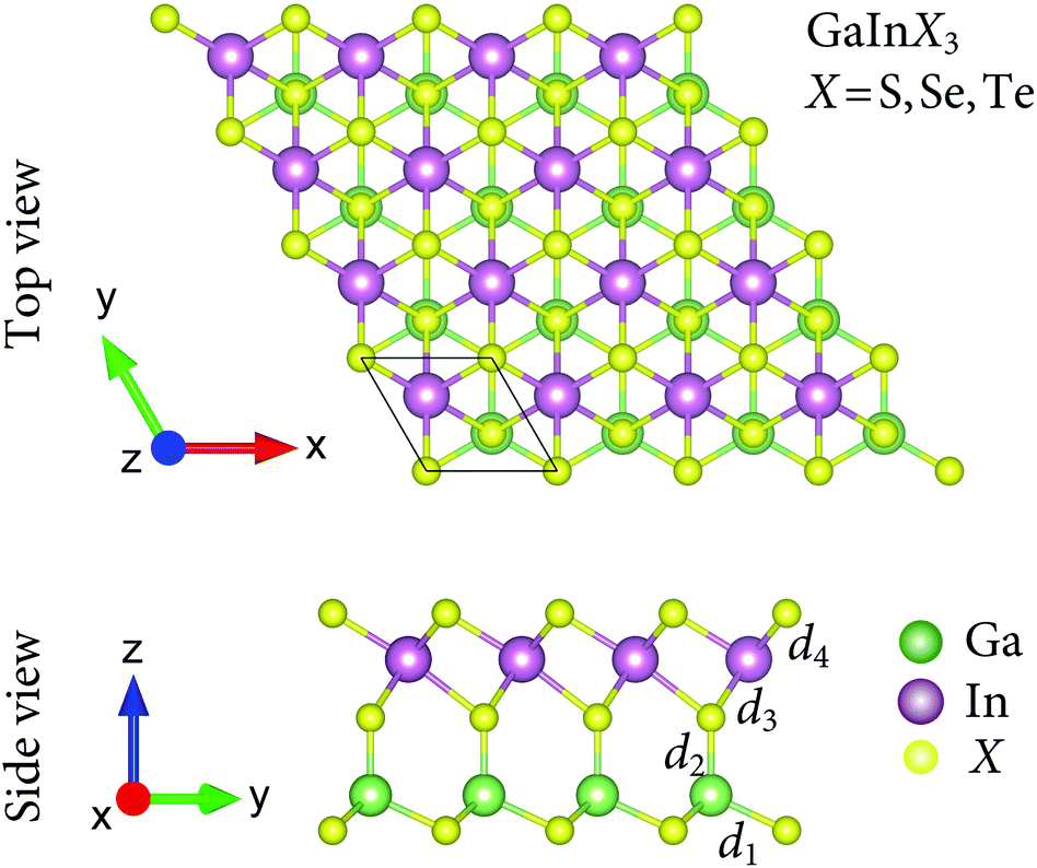 | ||
| Fig. 1 Top and side views of optimized atomic structures of the Janus GaInX3 (X = S, Se, Te) single-layers. The unit cell is indicated by a rhombus. | ||
| a (Å) | d1 (Å) | d2 (Å) | d3 (Å) | d4 (Å) | φ∠In–X–Ga (deg) | φ∠X–In–X (deg) | φ∠X–Ga–X (deg) | Δh (Å) | Ec (eV) | |
|---|---|---|---|---|---|---|---|---|---|---|
| GaInS3 | 3.74 | 2.38 | 2.21 | 2.73 | 2.53 | 127.68 | 95.47 | 103.38 | 6.20 | 4.35 |
| GaInSe3 | 3.90 | 2.52 | 2.34 | 2.84 | 2.66 | 127.53 | 94.40 | 101.92 | 6.60 | 3.95 |
| GaInTe3 | 4.19 | 2.71 | 2.55 | 3.04 | 2.87 | 127.30 | 93.71 | 101.23 | 7.17 | 3.49 |
To investigate the stabilities of the studied systems, we firstly examine the strength of chemical bonds via the analysis of their cohesive energy. In principle, GaInX3 can be constructed from Ga2X3, which has successfully been fabricated by experiment.6 Also, previous study suggested that Ga2X3 and In2X3 single layers are energetically favorable.10 The cohesive energy Ec of the Janus GaInX3 single-layers can be evaluated by:
 | (1) |
The obtained calculations for Ec of GaInX3 single-layers are summarized in Table 1. It is found that the cohesive energy of GaInX3 single-layers is quite high, from 3.49 to 4.35 eV per atom and these three structures of GaInX3 are confirmed to be energetically favorable. The cohesive energy Ec decreases as the atomic size of X element increasing.
Next, we calculate the phonon spectra to evaluate the dynamical stability of GaInX3 single-layers. The phonon spectra of GaInX3 single-layers, which are calculated by the DFPT method,21 are presented in Fig. 2. Note that the phonon splitting corrections23 are not included in the present calculations. There are five atoms in the primitive cell of GaInX3, therefore, its phonon dispersions contain 15 normal vibrational modes at the center of the Brillouin zone (the Γ point), including three acoustic modes in the low-frequency region and twelve optical modes in the higher frequency regions. It is known that the larger the mass atomic mass of elements, the softer the vibrations.24 Then, vibration frequencies in the phonon dispersions of GaInX3 are downshifted as the chalcogen element X changes from S to Te. As shown in Fig. 2, we can see that the phonon energies of GaInS3 single-layers are lower than those of GaInSe3 and GaInTe3 single-layers at the same point in the Brillouin zone. More importantly, there are no negative frequencies in the phonon dispersions of all three Janus GaInX3. The dynamic stabilities of materials were confirmed when the evaluated phonon dispersions contain only positive frequencies in the whole Brillouin zone. If the imaginary frequencies are available, the restoring force, which opposes the atom displacement of the atoms, will no longer exist. Obtained calculations for the phonon spectra, as depicted in Fig. 2, indicate that the Janus GaInX3 single-layers are dynamically stable.
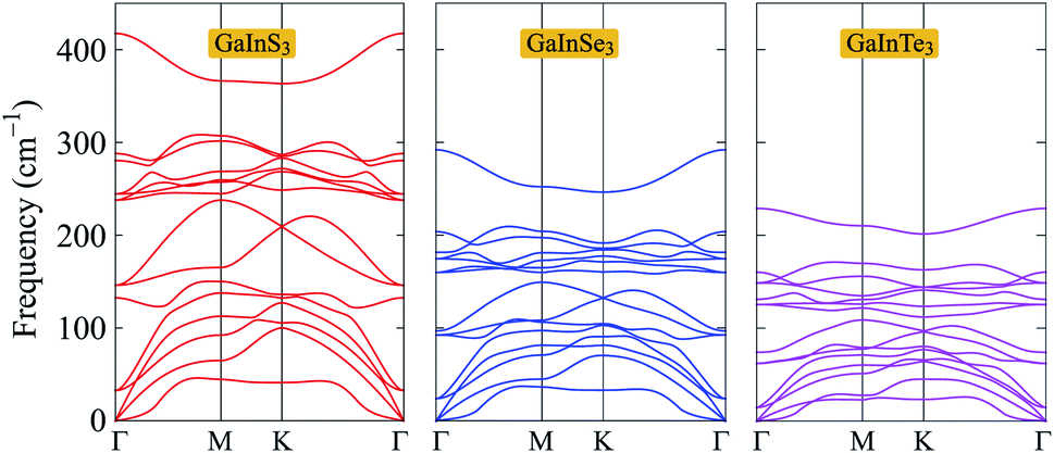 | ||
| Fig. 2 Phonon dispersions of GaInS3, GaInSe3, and GaInTe3 single-layers. | ||
Further, we examine the elastic characteristics to elucidate the mechanical stability of the considered Janus single-layers. The elastic constants can give important information about the mechanical stability of materials. The elastic constants Cij can be evaluated from the variation of energy when the small strains are applied to the equilibrium lattice state. With hexagonal structure as depicted in Fig. 1, only two independent elastic coefficients need to be estimated being C11 and C12 due to C11 = C22 and C66 = (C11 − C12)/2. The small range of uniaxial strain between −0.015 and 0.015 is applied to the x and y directions (each step being 0.005). The lattice structures at each value of applied strain are optimized and obtained coefficients are so-called relaxed-ion coefficients. By polynomial fitting the small strain-dependence of energy, we can get the coefficients C11 and C12.25 In Table 2, we summarized the calculated results for the elastic constants Cij of GaInX3 single-layers. It is demonstrated that the elastic constants of GaInX3 single-layers meet the Born's criteria for mechanical stability for hexagonal structures: C11 > 0 and C11 − C12 > 0.26

| C11 (N m−1) | C12 (N m−1) | C66 (N m−1) | Y2D (N m−1) |
|
|
|---|---|---|---|---|---|
| GaInS3 | 100.18 | 30.71 | 34.73 | 90.76 | 0.31 |
| GaInSe3 | 82.15 | 27.69 | 27.23 | 72.82 | 0.34 |
| GaInTe3 | 52.32 | 37.38 | 7.47 | 25.61 | 0.72 |

Young's modulus and Poisson's ratio depend greatly on the in-plane symmetric structure of the materials. The direction-dependence of Young's modulus Y2D(φ) and Poisson's ratio ν(φ) can be written as27,28
 | (2) |
 | (3) |
![[thin space (1/6-em)]](https://www.rsc.org/images/entities/char_2009.gif) φ, and c = cosφ. Here, φ is the angle between the armchair and investigated directions.
φ, and c = cosφ. Here, φ is the angle between the armchair and investigated directions.
The polar diagrams of Y2D(θ) and ν(θ) of GaInX3 single-layers are presented in Fig. 3. We can see that the direction-dependence of Y2D(θ) and ν(θ) are perfectly circulars. This suggests that GaInX3 single-layers show isotropic elastic characteristics. This is due to the 2D isotropic structures of GaInX2 as shown in Fig. 1. The Janus GaInX3 has a small Young's modulus, from 25.61 to 90.76 N m−1. Obviously, Young's modulus of GaInX3 is smaller than that of other available 2D structures, such as Janus MoSSe (113 N m−1)29 or MoS2 (130 N m−1).30 This indicates that the Janus GaInX3 single-layers are mechanically flexible materials and their mechanical strain threshold can be large.
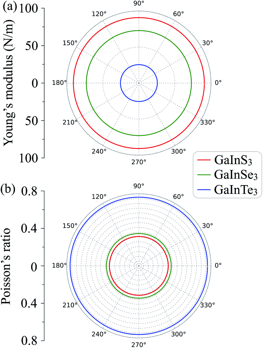 | ||
| Fig. 3 Direction-dependent Young's modulus (a) and Poisson's ratio (b) of GaInX3 single-layers. | ||
3.2 Electronic properties
In this section, we consider the electronic characteristics of the Janus GaInX3 single-layers. Band structures of GaInX3 are evaluated by using the PBE and HSE06 functionals as shown in Fig. 4. Our calculations indicate that all three configurations of GaInX3 are semiconductors. The electronic structures of 2D materials depend greatly on their geometry and structural parameters. At the PBE level, while GaInS3 and GaInSe3 single-layers exhibit the direct semiconducting characters, GaInTe3 has an indirect bandgap with the conduction band minimum (CBM) lying at the Γ point and the valence band maximum (VBM) being on the ΓM-path. The PBE bandgap EPBEg of GaInX3 reduces from 0.93 to 0.25 eV as the chalcogen element X changing from S to Te as listed in Table 3. The calculated band structures of GaInX3 single-layers are also shown in Fig. 4. The band diagrams calculated by the PBE and HSE methods have almost the same profile. The bandgap calculated by the HSE06 functional, however, is wider than the PBE bandgap. The bandgap calculated by the HSE06 method is considered to be more accurate than the PBE method. Our calculated results indicated that the HSE06 bandgap EPBEg of GaInX3 single-layers is in the interval between 0.75 and 1.64 eV.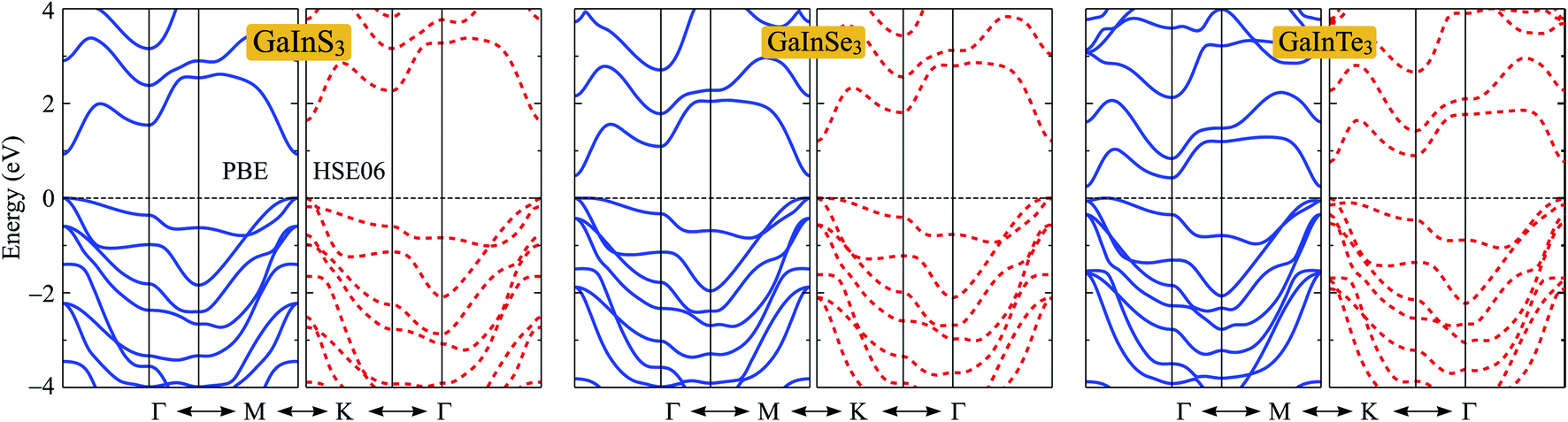 | ||
| Fig. 4 Band structures along the high-symmetry direction Γ–M–K–Γ of Janus GaInX3 (X = S, Se, Te) single-layers at the PBE (solid lines) and HSE06 (dashed lines) levels. | ||
| EPBEg | EHSE06g | EF | ΔΦ | Φ1 | Φ2 | |
|---|---|---|---|---|---|---|
| GaInS3 | 0.93 | 1.64 | −2.08 | 1.65 | 4.88 | 6.53 |
| GaInSe3 | 0.47 | 1.20 | −2.01 | 1.29 | 4.53 | 5.83 |
| GaInTe3 | 0.25 | 0.75 | −1.18 | 0.90 | 4.16 | 5.06 |
To get more insights into the nature of the energy bands of the considered structures, we evaluate the weighted band of GaInX3 single-layers at the HSE06 level as revealed in Fig. 5. There are similarities in the weighted bands between the Janus GaInX3 single-layers. It is demonstrated that the VBM of GaInX3 is mainly contributed from the p-orbitals of the chalcogen atom X. Meanwhile, Ga-s orbitals have a largely contribution to the CBM of GaInX3. The contribution of the orbitals of Ga and In atoms to the valence band is much smaller than that of the X-p orbitals. Also, the X-p orbitals also make a important contribution to the conduction band in the high-energy region.
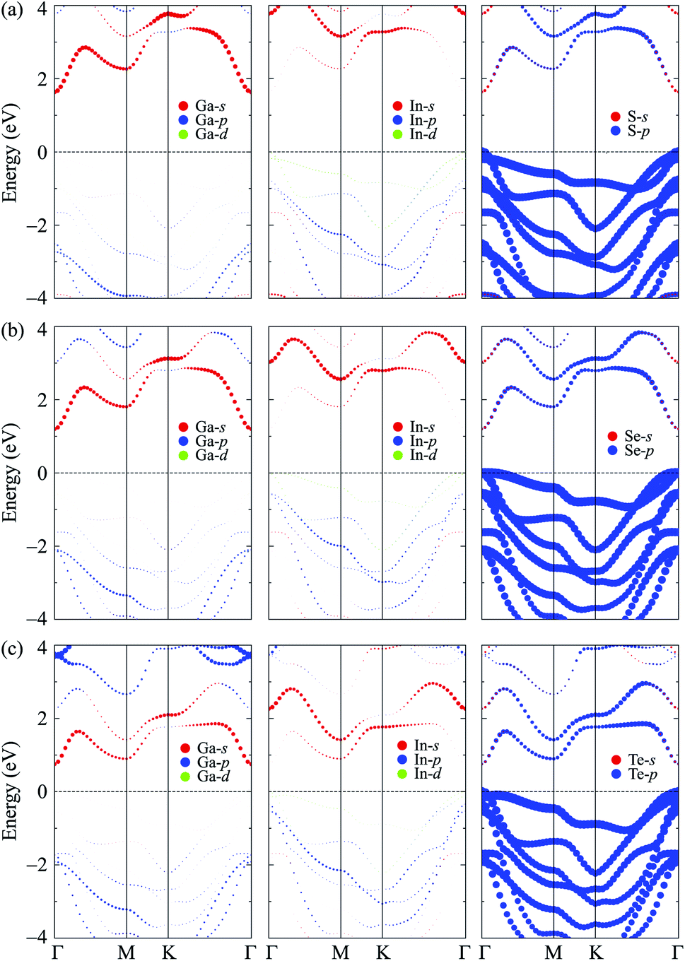 | ||
| Fig. 5 Weighted bands of GaInS3 (a), GaInSe3 (b), and GaInTe3 (c) single-layers at the HSE06 level. | ||
One of the more important properties of electrons that we need to investigate is the work function. The work function Φ is calculated based on the formula as: Φ = Evac − EF. Here, Evac and EF are the vacuum and Fermi levels, which can obtain by calculating the electrostatic potential of the material. Due to the vertical asymmetric structure, Janus single-layers possess an intrinsic built-in electric field as previously reported by Fu and co-workers.7 Therefore, we include the dipole correction in the present calculations to treat the possible errors induced by the periodic boundary condition.31 The electrostatic potential of the Janus GaInX3 single-layers with dipole correction are depicted in Fig. 6. As predicted, a distinct vacuum level difference ΔΦ between the two sides has been found in the Janus GaInX3 structures. Our calculations reveal that the ΔΦ of GaInX3 reduces when the atomic size of X element increases. As summarized in Table 3, the vacuum level difference ΔΦ of GaInX3 is from 0.90 to 1.65 eV. As a result, there is a difference between the work functions on the two different sides of GaInX3. The calculated work functions on the XGa-side Φ1 and InX-side Φ2 of GaInX3 single-layers are tabled in Table 3. We can see that, in each single-layer, Φ1 is always smaller than Φ2. This suggests that electrons can escape from the XGa-surface more easily than the InX-surface. Besides, the difference in the vacuum level leads to the difference in the photocatalytic performance at the two different surfaces of the Janus structures.
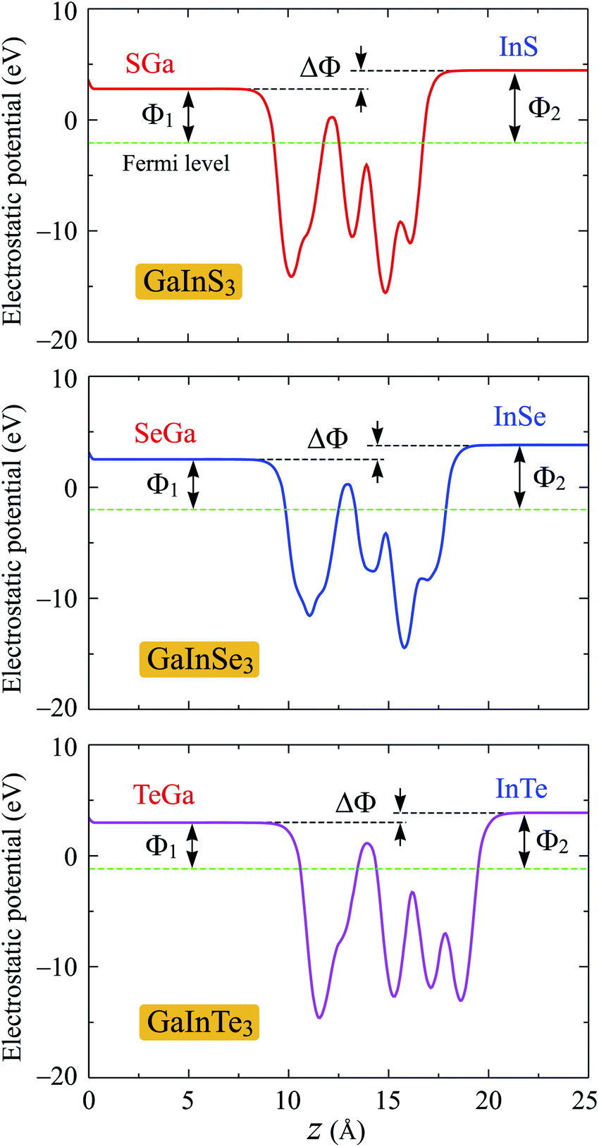 | ||
| Fig. 6 Planar electrostatic potential of the Janus GaInX3 (X = S, Se, Te) single-layers with dipole correction. ΔΦ is the difference in the vacuum levels between the XGa and InX sides. | ||
3.3 Transport properties
To evaluate the potential application of materials in electronic devices, we need to examine their transport properties. We here focus on the characteristics of carrier mobility, which are the most important characteristics of the transport properties. The carrier mobility of materials can be investigated by the deformation potential approximation.22 The mobility of the carriers for the 2D materials can be expressed in the form:32
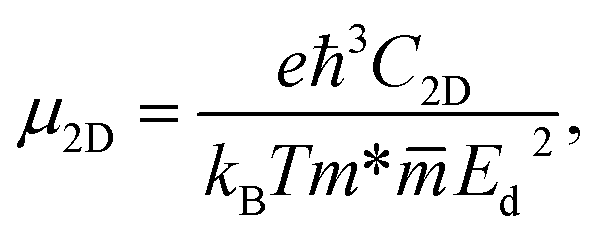 | (4) |
 is the average effective mass. The calculations for the carrier mobility were performed at room temperature (T = 300 K). The transport characteristics were investigated along the two transport directions.
To calculate the carrier mobility μ2D as expressed in eqn (4), we first evaluate the effective mass of carriers, which strongly affects the mobilities of carriers. The effective masses of carriers can be attained by fitting parabolic function to the CBM (electron) and VBM (hole) via the formula as follows:
 | (5) |
The effective masses of carriers of GaInX3 single-layers are summarized in Table 4. It is found that the effective mass of both electron and hole is highly directional isotropic. This is due to the in-plane isotropic lattice of the Janus GaInX3 single-layers. However, the effective mass of the electron is much smaller than that of hole, particularly in the case of GaInS3 single-layer. The smaller the carrier mass, the faster carriers respond to the external field, and as a result, they have high mobility. As listed in Table 4, we can see that GaInTe3 has the smallest electron effective mas, 0.15 m0. The electron effective mass of GaInS3 and GaInTe3 is found to be 0.29 m0 and 0.18 m0, respectively.
|
|
C2Dx | C2Dy | Edx | Edy | μx | μy | ||
|---|---|---|---|---|---|---|---|---|---|
| GaInS3 | Electron | 0.29 | 0.29 | 66.57 | 66.58 | −9.12 | −9.12 | 202.87 | 203.08 |
| Hole | 2.69 | 2.69 | 66.57 | 66.58 | −7.51 | −7.59 | 3.20 | 3.13 | |
| GaInSe3 | Electron | 0.18 | 0.18 | 54.84 | 54.86 | −8.01 | −8.01 | 580.82 | 580.55 |
| Hole | 0.47 | 0.47 | 54.84 | 54.86 | −7.33 | −7.42 | 22.88 | 22.33 | |
| GaInTe3 | Electron | 0.15 | 0.15 | 43.38 | 43.43 | −8.70 | −8.69 | 530.03 | 532.18 |
| Hole | 0.23 | 0.23 | 43.38 | 43.43 | −7.82 | −7.98 | 117.52 | 113.06 |
Along with the effective mass, the carrier mobility depends also on the elastic modulus C2D and deformation potential constant Ed as presented in eqn (4). The elastic modulus C2D is given by
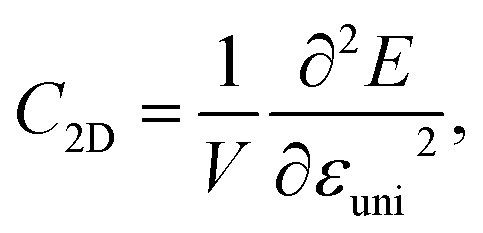 | (6) |
The deformation potential constant Ed is written in the form:
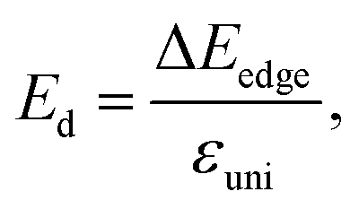 | (7) |
The strain-dependent energy change and band edge positions of all three Janus structures GaInX3 are shown in Fig. 7. It is found that there is no significant difference in elastic modulus along the x and y directions in each single-layer. The deformation potential constant of GaInX3 is also high directional isotropic. This is also due to the in-plane isotropic lattice of the investigated systems. However, there is a small difference in the Ed of electron and hole in all three investigated structures. The calculated results for the C2D and Ed are summarized in Table 4.
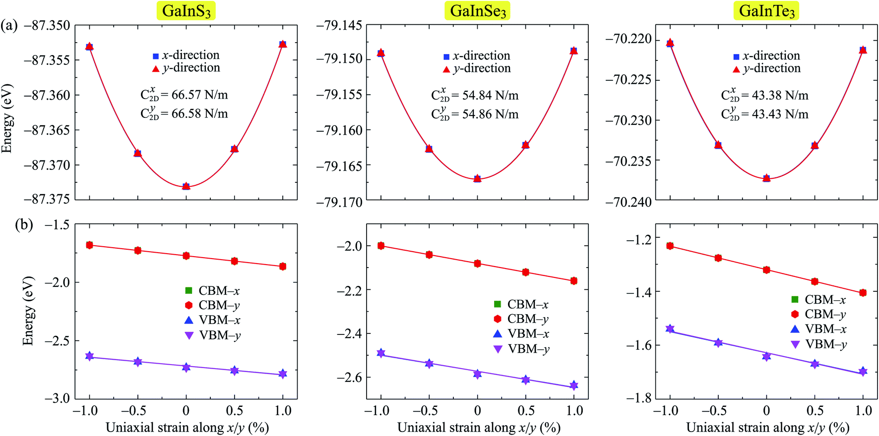 | ||
| Fig. 7 Strain-dependent total energy (a) and band-edge positions (b) of GaInX3 single-layers along two transport directions x and y. | ||
In Table 4, we list the calculated results for the carrier mobility of GaInX3 single-layers along the two transport directions. It is found that the mobility of both electron and hole of GaInX3 is highly directional isotropic. There is no significant difference between carrier mobilities along the x and y directions. Due to the largely difference in the effective mass and also deformation potential constant between electron and hole, it is calculated that the electron mobility is much higher than that the hole mobility. The electron mobility of GaInSe3 is calculated to be up to about 580 cm2 V−1 s−1 and all Janus GaInX3 structures possess electron mobility in excess of 200 cm2 V−1 s−1. It is also worth noting that, with electron mobility of about 200 cm2 V−1 s−1, MoS2 was able to perfectly apply to high-performance electronic devices as previously reported by Radisavljevic and co-workers.34 This suggests that the Janus GaInX3 single-layer could be potential materials for applications in nanoelectronic devices.
4 Conclusion
In this paper, we systematically considered the structural, electronic, and transport properties of the novel Janus GaInX3 single-layers using the DFT calculations. The obtained results indicated that the structure of Janus GaInX3 single-layers was confirmed to be stable and their elastic properties are highly directional isotropic. At the equilibrium states, GaIn3 single-layers are semiconductors with a small bandgap. Due to the asymmetric structure, there exists a distinct vacuum level difference on the two sides of the Janus GaInX3. Carrier mobility of GaInX3 is also highly isotropic along the two transport directions and their electron mobility can be up to about 580 cm2 V−1 s−1, which is suitable for applications in nanoelectronics.Conflicts of interest
There are no conflicts to declare.Acknowledgements
This work is funded by the Vietnam Ministry of Education and Training under Grant No. B2022-DNA-14.References
- N. A. Poklonski, S. A. Vyrko, A. I. Siahlo, O. N. Poklonskaya, S. V. Ratkevich, N. N. Hieu and A. A. Kocherzhenko, Mater. Res. Express, 2019, 6, 042002 CrossRef.
- T. V. Vu, C. V. Nguyen, H. V. Phuc, A. A. Lavrentyev, O. Y. Khyzhun, N. V. Hieu, M. M. Obeid, D. P. Rai, H. D. Tong and N. N. Hieu, Phys. Rev. B, 2021, 103, 085422 CrossRef CAS.
- T. V. Vu, V. T. T. Vi, H. V. Phuc, A. I. Kartamyshev and N. N. Hieu, Phys. Rev. B, 2021, 104, 115410 CrossRef CAS.
- T. N. Bich, S. S. Kubakaddi, L. Dinh, N. N. Hieu and H. V. Phuc, Phys. Rev. B, 2021, 103, 235417 CrossRef CAS.
- A.-Y. Lu, H. Zhu, J. Xiao, C.-P. Chuu, Y. Han, M.-H. Chiu, C.-C. Cheng, C.-W. Yang, K.-H. Wei, Y. Yang, Y. Wang, D. Sokaras, D. Nordlund, P. Yang, D. A. Muller, M.-Y. Chou, X. Zhang and L.-J. Li, Nat. Nanotechnol., 2017, 12, 744 CrossRef CAS PubMed.
- G. Almeida, S. Dogan, G. Bertoni, C. Giannini, R. Gaspari, S. Perissinotto, R. Krahne, S. Ghosh and L. Manna, J. Am. Chem. Soc., 2017, 139, 3005–3011 CrossRef CAS PubMed.
- C.-F. Fu, J. Sun, Q. Luo, X. Li, W. Hu and J. Yang, Nano Lett., 2018, 18, 6312–6317 CrossRef CAS PubMed.
- P. Zhao, Y. Ma, X. Lv, M. Li, B. Huang and Y. Dai, Nano Energy, 2018, 51, 533–538 CrossRef CAS.
- J. Xiao, H. Zhu, Y. Wang, W. Feng, Y. Hu, A. Dasgupta, Y. Han, Y. Wang, D. A. Muller, L. W. Martin, P. Hu and X. Zhang, Phys. Rev. Lett., 2018, 120, 227601 CrossRef CAS PubMed.
- L. Hu and X. Huang, RSC Adv., 2017, 7, 55034–55043 RSC.
- G. Liu, Z. Zhang, H. Wang, G.-L. Li, J.-S. Wang and Z. Gao, J. Appl. Phys., 2021, 130, 105106 CrossRef CAS.
- J. Zhao, X. Huang, Y. Yin, Y. Liao, H. Mo, Q. Qian, Y. Guo, X. Chen, Z. Zhang and M. Hua, J. Phys. Chem. Lett., 2021, 12, 5813–5820 CrossRef CAS PubMed.
- W. Ding, J. Zhu, Z. Wang, Y. Gao, D. Xiao, Y. Gu, Z. Zhang and W. Zhu, Nat. Commun., 2017, 8, 14956 CrossRef CAS PubMed.
- P. Wang, H. Liu, Y. Zong, H. Wen, J.-B. Xia and H.-B. Wu, ACS Appl. Mater. Interfaces, 2021, 13, 34178–34187 CrossRef CAS PubMed.
- T. V. Vu and N. N. Hieu, J. Phys.: Condens. Matter, 2022, 34, 115601 CrossRef PubMed.
- P. Giannozzi, S. Baroni, N. Bonini, M. Calandra, R. Car, C. Cavazzoni, D. Ceresoli, G. L. Chiarotti, M. Cococcioni, I. Dabo, A. D. Corso, S. de Gironcoli, S. Fabris, G. Fratesi, R. Gebauer, U. Gerstmann, C. Gougoussis, A. Kokalj, M. Lazzeri, L. Martin-Samos, N. Marzari, F. Mauri, R. Mazzarello, S. Paolini, A. Pasquarello, L. Paulatto, C. Sbraccia, S. Scandolo, G. Sclauzero, A. P. Seitsonen, A. Smogunov, P. Umari and R. M. Wentzcovitch, J. Phys.: Condens. Matter, 2009, 21, 395502 CrossRef PubMed.
- P. E. Blöchl, Phys. Rev. B: Condens. Matter Mater. Phys., 1994, 50, 17953 CrossRef PubMed.
- J. P. Perdew, K. Burke and M. Ernzerhof, Phys. Rev. Lett., 1996, 77, 3865 CrossRef CAS PubMed.
- J. Heyd, G. E. Scuseria and M. Ernzerhof, J. Chem. Phys., 2003, 118, 8207 CrossRef CAS.
- S. Grimme, J. Comput. Chem., 2006, 27, 1787 CrossRef CAS PubMed.
- T. Sohier, M. Calandra and F. Mauri, Phys. Rev. B, 2017, 96, 075448 CrossRef.
- J. Bardeen and W. Shockley, Phys. Rev., 1950, 80, 72 CrossRef CAS.
- T. Sohier, M. Gibertini, M. Calandra, F. Mauri and N. Marzari, Nano Lett., 2017, 17, 3758–3763 CrossRef CAS PubMed.
- A. Molina-Sánchez and L. Wirtz, Phys. Rev. B: Condens. Matter Mater. Phys., 2011, 84, 155413 CrossRef.
- K.-A. N. Duerloo, M. T. Ong and E. J. Reed, J. Phys. Chem. Lett., 2012, 3, 2871–2876 CrossRef CAS.
- R. C. Andrew, R. E. Mapasha, A. M. Ukpong and N. Chetty, Phys. Rev. B: Condens. Matter Mater. Phys., 2012, 85, 125428 CrossRef.
- N. T. Hung, A. R. T. Nugraha and R. Saito, J. Phys. D: Appl. Phys., 2018, 51, 075306 CrossRef.
- P. Xiang, S. Sharma, Z. M. Wang, J. Wu and U. Schwingenschlögl, ACS Appl. Mater. Interfaces, 2020, 12, 30731 CrossRef CAS PubMed.
- S.-D. Guo, Phys. Chem. Chem. Phys., 2018, 20, 7236–7242 RSC.
- R. C. Cooper, C. Lee, C. A. Marianetti, X. Wei, J. Hone and J. W. Kysar, Phys. Rev. B: Condens. Matter Mater. Phys., 2013, 87, 035423 CrossRef.
- L. Bengtsson, Phys. Rev. B: Condens. Matter Mater. Phys., 1999, 59, 12301 CrossRef CAS.
- W. Wan, S. Zhao, Y. Ge and Y. Liu, J. Phys.: Conden. Matter, 2019, 31, 435501 CrossRef CAS PubMed.
- S.-D. Guo, W.-Q. Mu, Y.-T. Zhu, R.-Y. Han and W.-C. Ren, J. Mater. Chem. C, 2021, 9, 2464–2473 RSC.
- B. Radisavljevic, A. Radenovic, J. Brivio, V. Giacometti and A. Kis, Nat. Nanotechnol., 2011, 6, 147–150 CrossRef CAS PubMed.
| This journal is © The Royal Society of Chemistry 2022 |