
 Open Access Article
 This Open Access Article is licensed under a Creative Commons Attribution-Non Commercial 3.0 Unported Licence
Effect of BaTiO3 powder as an additive in perovskite films on solar cells
Chuanxiang Zhang a,
Xiqiang Lib,
Lingling Dingb,
Chen Jina and
Haijun Tao*b
a,
Xiqiang Lib,
Lingling Dingb,
Chen Jina and
Haijun Tao*b
aSchool of Materials Science and Engineering, Nanjing Institute of Technology, Nanjing 211167, China
bCollege of Materials Science and Technology, Nanjing University of Aeronautics and Astronautics, Nanjing 211106, China. E-mail: taohaijun@nuaa.edu.cn
First published on 10th March 2022
Abstract
Perovskite solar cells (PSCs) are considered to be ideal energy devices, where perovskite-type organic metal halides act as light-absorbing materials. In PSCs, the photoexcitons are extracted and separated to afford high photoelectric conversion efficiency under the action of the built-in electric field (Ebi). However, the current challenge is that a low Ebi cannot provide a sufficient driving force to separate photonic excitons, which causes the captured charges to escape from the deep energy-level defect state. Here, the ferroelectric material barium titanate (BaTiO3) was directly introduced into the perovskite precursor solution to reduce the defection density (to 8.58 × 1017 cm−3) in PSCs and promote the separation of photoexcitons. Furthermore, the addition of BaTiO3 improved the quality of the perovskite film and significantly increased the photoelectric performance after the polarization treatment. This is mainly attributed to the residual polarization electric field generated by ferroelectric polarization, which increased the Ebi of the PSCs and the width of the depletion layer and inhibited the non-radiative recombination of carriers. This work provides a possibility to design and develop optoelectronic devices with high-efficiency optoelectronic response behavior.
1 Introduction
Organic–inorganic hybrid perovskite (OIHP) materials have become a bright-star material because of their excellent optical and electrical properties and simple and low-cost synthetic methods. Since the first report from Miyasaka's research group in 2009, the photoelectric conversion efficiency (PCE) of PSCs has rapidly increased from an initial 3.8% (ref. 1) to a certified 25.5% (ref. 2) in just ten years. Despite this rapid development, the PCE of PSCs is still far below the S–Q limitation (33.5%) of single-junction solar cells due to the non-radiative recombination of carriers in PSCs. The main causes of carrier recombination are poor quality of the perovskite film, material interface mismatch, and low built-in electric field. At present, the first two factors are mainly investigated and analyzed in view of perovskite crystallization engineering, defect passivation engineering, and interface engineering,3–6 whereas studies on improving cell performance based on increasing Ebi are still few. Therefore, when other optimization methods cannot further improve the overall performance of PSCs, we consider that carrier separation and transmission can be regulated by enhancing the Ebi with the aim of reducing the occurrence of non-radiative recombination.The first method to increase the Ebi of the cell is to apply an external electric field on the photoactive layer of photovoltaic devices to suppress carrier recombination at the capture site. Chen et al.7 first proved the ferroelectric property of MAPbI3 through the phase change of the piezoelectric microscope (PFM), and further verified that pressurized polarization can regulate the interface energy-band structures of PSCs for charge separation under certain circumstances. Zhang et al.8 developed an external electric field-assisted annealing treatment technology, which can control the ion polarization direction of perovskite films. Therefore, a good perovskite crystal film obviously enhances the internal electric field and effectively promotes charge separation and transport, leading to an increase in the PCE of PSCs from 16.77% to 19.18%. This method of carrier transport assisted by an external electric field mainly relies on the recognition of the ferroelectric properties of OIHP materials. Although researchers have confirmed this conclusion by theoretical calculation,9–11 PFM observation,7 and hysteresis loop measurement (P–E),12,13 Fan et al.14 did not observe the existence of ferroelectric domains in MAPbI3, and the P–E test results also showed that MAPbI3 did not have ferroelectric properties. Therefore, whether this material has ferroelectricity is still controversial. Since it is impossible to determine whether the ferroelectricity of MAPbI3 exists or not, we should focus on the utilization of the electric field to promote carrier separation. However, it is not difficult to understand that this is not a persistent and stable method because the applied electric field is easily shielded by ion migration or accumulated charges. On this basis, we hope to develop a material that can maintain permanent polarization and provide a stable and controllable electric field for optoelectronic devices.
Based on the knowledge of ferroelectric materials, we think about their residual polarization field. Ferroelectric materials are introduced into the PSCs to change the remaining polarization electric field through the external electric field, finally regulating the ion and carrier transports. This idea was firstly used in the fields of photovoltaic organic solar cells (OPV) and dye sensitized solar cells (DSSC). Researchers introduced inorganic ferroelectric materials (SrTiO3, BaTiO3, etc.) and organic ferroelectric materials [PVDF, P(VDF-TrFE), etc.] into OPV light absorption layer, anionic buffer layer, and photoanode of DSSC, respectively, causing better photoelectric performance.15–18 PSCs are developed from DSSC with similar principles. In view of the successful application of ferroelectric materials in DSSC, researchers are aiming at introducing ferroelectric materials into PSCs to further improve their efficiency.19–24 At present, the introduction of ferroelectric materials has three locations or functions: replacing TiO2 as ETL, inserting at the ETL/perovskite layer or the perovskite/HTL interface, and forming the perovskite layer. The former two methods are common, and the latter method is only used for organic materials P(VDF-TrFE).
In this work, in order to improve the Ebi of PSCs, we selected the inorganic ferroelectric material, BaTiO3, which induced strong spontaneous polarization and had the same structure as that of the perovskite film to prepare the composite optical absorption layer. Subsequently, the corresponding microstructures and chemical compositions were characterized in detail to support the mechanistic analyses on the carrier transport. Also, the photoelectric performance of the PSCs with the introduction of ferroelectric materials was measured around the two aspects of photoelectric conversion efficiency and interfacial state. This work will provide a possibility to design and develop optoelectronic devices with high-efficiency optoelectronic response behavior.
2 Experimental
2.1 Materials
Isopropyl titanate (99%), titanium tetrachloride (99%), chlorobenzene (99.5%), isopropanol (99.8%), barium titanate (<100 nm, 99.9%), and graphite (8000 mesh, 99.95%) were all purchased from Aladdin Reagent (Shanghai) Co., Ltd. Lead iodide (99%), dimethyl sulfoxide (DMSO, 99%), and N,N-dimethylformamide (DMF, 99.9%) were all purchased from Sigma-Aldrich. Ethyl cellulose (CP, M70) was provided by Sinopharm Chemical Reagents Co. Ltd. Carbon black (30–45 nm) was purchased from Nanjing Xianfeng Nano Co., Ltd; TiO2 slurry (NJV-30NR-D) and ammonium methyl iodide (99%) were provided by Sunlight New Energy Co., Ltd and Maitidevi Chemical New Material Technology Co., Ltd, respectively. The FTO conductive glasses with the resistance of 7–8 Ω □−1 were provided by Shandong Opivite New Energy Technology Co., Ltd.2.2 BaTiO3@MAPbI3 precursor solution preparation
Firstly, 3000 μL mixed solution of DMF and DMSO (volume ratio of 4![[thin space (1/6-em)]](https://www.rsc.org/images/entities/char_2009.gif) :1) was prepared and placed in bottle A for later use. 40 mg BaTiO3 powders were accurately weighed and placed into bottle B, where the above mixed solution (1000 μL) in bottle A was added. Then, the ultrasonic treatment was carried out until the powders were evenly dispersed into the solution. Subsequently, 1500 μL mixed solution of DMF and DMSO was sucked into bottle C, where 2.4 M MAI and PbI2 were added.
:1) was prepared and placed in bottle A for later use. 40 mg BaTiO3 powders were accurately weighed and placed into bottle B, where the above mixed solution (1000 μL) in bottle A was added. Then, the ultrasonic treatment was carried out until the powders were evenly dispersed into the solution. Subsequently, 1500 μL mixed solution of DMF and DMSO was sucked into bottle C, where 2.4 M MAI and PbI2 were added.
For 0.5 wt% BaTiO3@MAPbI3 precursor solution, we took 300 μL of the solution in bottle A, 100 μL of the solution of bottle B, and 400 μL of the solution of bottle C to form the precursor solution. Also, the mixed solution including 200 μL bottle A solution, 200 μL bottle B solution, and 400 μL bottle C solution could form 1.0 wt% BaTiO3@MAPbI3 precursor solution. The 2.0 wt% BaTiO3@MAPbI3 precursor solution included 400 μL solution of bottle B and 400 μL solution of bottle C. All these precursor solutions would be stirred at 60 °C for use in device fabrication.
2.3 Device fabrication
After cleaning the FTO conductive glasses, we coated their surfaces with the compact layer solution at 2000 rpm for 60 s, which was followed by heat treatment at 500 °C for 30 min. The TiO2 precursor was prepared by diluting TiO2 slurry with alcohol at a mass ratio of 1:7, then it was spun onto the surface of the above compact layer at the speed of 3000 rpm for 30 s. Also, the as-prepared TiO2 precursor was treated at 500 °C for 30 min. The prepared FTO conductive glasses were immersed in TiCl4 solution, soaked at 70 °C for 30 min, and then treated at 500 °C for 30 min. The as-prepared BaTiO3@MAPbI3 precursor was spin-coated onto the surface of the modified layer by a two-step spin-coating method (1000 rpm, 10 s and 5000 rpm, 30 s). 250 μL chlorobenzene was dripped onto the spin-coated film. Afterward, annealing treatment was carried out on the heating platform in two steps (60 °C, 2 min; 120 °C, 10 min). Finally, the carbon slurry (including ethyl cellulose, carbon black, graphite, ethyl cellulose solution, and chlorobenzene) was scraped onto the surface of the perovskite layer and annealed at 100 °C for 1 h to complete the assembly of the whole cell. Also, the whole assembly process of the cell was completed in air. The fabrication process of the BaTiO3@MAPbI3 composite film with a certain content (0.5 wt%, 1.0 wt%, and 2.0 wt%) of BaTiO3 powders in the perovskite precursor solution, as shown in Fig. 1.
 | ||
| Fig. 1 BaTiO3@MAPbI3 composite film and the device preparation processes. | ||
2.4 Characterization
X-ray diffraction (XRD, RIGAKU Ultima IV) was used to characterize the crystal structure of the samples. Spectroscopy (Renishaw in Via) was used to characterize the phase structure of BaTiO3 nanoparticles. Field emission scanning electron microscopy (FE-SEM, Zeiss Merlin Compact) was used to characterize the surface and section morphologies. The J–V characteristic curves of C-PSCs were obtained using the full spectrum solar simulator (Model 91192, Newport Co.), equipped with a Keithley digital source meter (Keithley 2400), and the effective area was set to 0.15 cm2. The EQE characterization of the C-PSCs was carried out by an external quantum test system (Oriel's IQE 200) in the wavelength range of 300–900 nm.An electrochemical workstation (Shanghai Chenhua C660E) was used to evaluate the corresponding electrochemical performances. The electrochemical impedance test amplitude was 10 mV with test frequency in the range of 1–1 MHz, and the Mott–Schottky test frequency of 10 kHz. The excitation voltage of the photoluminescence test system (PTI QM40-NI) was 3 V, the light source wavelength in the system was 355 nm, and the test wavelength range was 650–850 nm. All the characterizations were carried out in the atmosphere without any encapsulation.
3 Results and discussion
From the point-view of the structural features, ferroelectricity is an electron/ion polarization phenomenon in the typical perovskite BaTiO3 materials, which is caused by the displacement of the Ti4+ cation in the TiO6 octahedron from the center. This process results in a decrease in the symmetry between the unit cell and the cubic lattice, and the structural transformation from the cubic phase to the tetragonal phase. Also, the phase structure directly determines the ferroelectricity of BaTiO3; therefore, it needed to analyze the crystal structures of BaTiO3 materials.Tetragonal BaTiO3 (T-BaTiO3) nanoparticles were prepared by the simple sintering treatment on cubic BaTiO3 (C-BaTiO3) nanoparticles at 800 °C.25 Firstly, the crystal structures of the two BaTiO3 were verified by XRD, as shown in Fig. 2(a). C-BaTiO3 shows a single peak at 2θ = 45° corresponding to the (200) crystal plane, which is consistent with the cubic BaTiO3 structure of the Pm![[3 with combining macron]](https://www.rsc.org/images/entities/char_0033_0304.gif) m space group (JCPDS no. 79-2263). On the other hand, the splitting phenomenon of the peak of T-BaTiO3 is also observed at the position of about 2θ = 45° (upper right inset), where 44.8° and 45.2° correspond to the (002) and (200) crystal planes of BaTiO3, respectively. It matches well with the tetragonal BaTiO3 structure (JCPDS no. 05-0626). Raman spectroscopy is an advantageous technique to analyze the cubic-tetragonal symmetry of BaTiO3 nanoparticles. Fig. 2(b) shows the Raman spectrum of the BaTiO3 powders after sintering. Among them, the two Raman peaks at 305 cm−1 and 717 cm−1 are the characteristic peaks of tetragonal BaTiO3, indicating that T-BaTiO3 has a tetragonal crystal structure at room temperature.26
m space group (JCPDS no. 79-2263). On the other hand, the splitting phenomenon of the peak of T-BaTiO3 is also observed at the position of about 2θ = 45° (upper right inset), where 44.8° and 45.2° correspond to the (002) and (200) crystal planes of BaTiO3, respectively. It matches well with the tetragonal BaTiO3 structure (JCPDS no. 05-0626). Raman spectroscopy is an advantageous technique to analyze the cubic-tetragonal symmetry of BaTiO3 nanoparticles. Fig. 2(b) shows the Raman spectrum of the BaTiO3 powders after sintering. Among them, the two Raman peaks at 305 cm−1 and 717 cm−1 are the characteristic peaks of tetragonal BaTiO3, indicating that T-BaTiO3 has a tetragonal crystal structure at room temperature.26
 | ||
| Fig. 2 (a) XRD patterns of BaTiO3 powders before and after sintering. (b) Raman spectrum of BaTiO3 powders after sintering. | ||
As shown in Fig. 3(a and b), it can be obviously seen that there are many pinholes on the surface of the film without the addition of BaTiO3, and many white spots are distributed at the grain boundaries. According to the literature reports, it can be determined that these white spots are residual PbI2.27 After adding BaTiO3, the pinholes on the surface of the MAPbI3 film disappeared, the surface was uniform and dense, and the number of small white particles also decreased to a certain extent. The average grain size of MAPbI3 increased from 0.47 μm to 0.51 μm. The main reason was that both BaTiO3 and MAPbI3 had an octahedral structure. A similar structure allows BaTiO3 to be used as the seed layer to induce the crystal growth of the MAPbI3 film, and the crystal grain size increases significantly. Since the grain boundary in the MAPbI3 film can be used as a trap center, it is an important factor to cause the non-radiative recombination of carriers.28 Therefore, the increase in the crystal grain size can effectively suppress the occurrence of non-radiative recombination and increase the open circuit voltage and filling factor of the device. Fig. 3(c and d) shows the cross-sectional views of the sample before and after the addition of BaTiO3. It can be seen that the thickness of the perovskite layer does not change significantly. When BaTiO3 is not added, there is a large gap between the MAPbI3 film and the substrate, causing the interruption of the carrier transport channel and adversely affect the carrier transport. The addition of BaTiO3 completely covers the substrate, which is conducive for the transport of carriers. At the same time, it can be seen that the surface of the MAPbI3 film with BaTiO3 is smoother without obvious protrusions. The relatively smooth surface can also improve the interface contact between the MAPbI3 film and the carbon electrode, promoting the transfer of holes, and effectively inhibiting carrier recombination. However, it is not the main factor affecting the inhibition of carrier recombination, compared with the addition of BaTiO3.
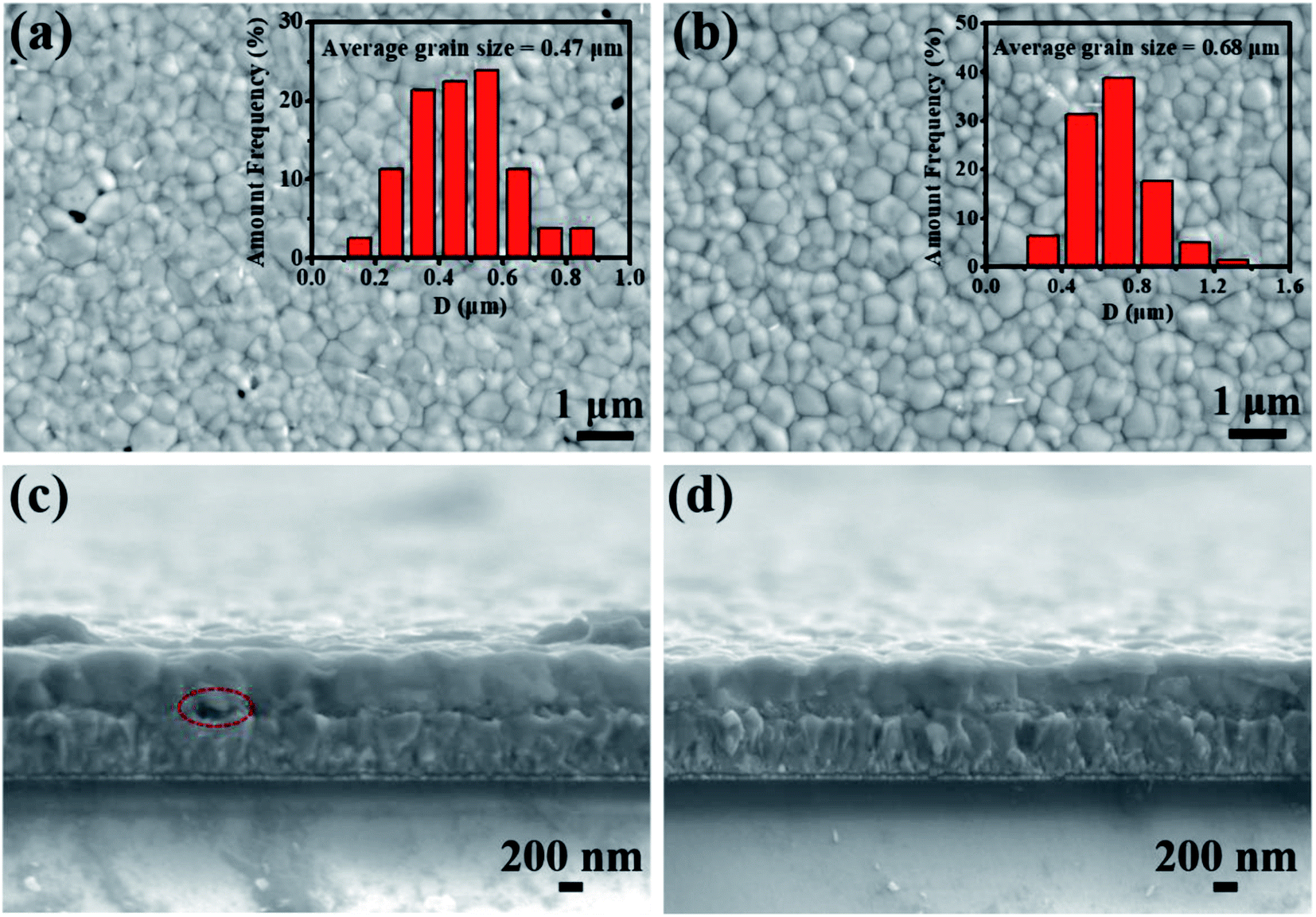 | ||
| Fig. 3 FE-SEM images of (a) FTO/TiO2/MAPbI3 and (b) FTO/TiO2/BaTiO3:MAPbI3. Cross section images of (c) FTO/TiO2/MAPbI3 and (d) FTO/TiO2/BaTiO3:MAPbI3. The insets in (a) and (b) are the grain size distributions of the corresponding samples. | ||
In order to investigate the influence of the BaTiO3 doping amount on the crystallization properties of the MAPbI3 film, the XRD diffraction pattern was used to characterize the film, as shown in Fig. 4(a). The film has two strong diffraction peaks at 14.11° and 28.45°, corresponding to the MAPbI3 (110) and (202) crystal planes. The results show that no new diffraction peaks appear at the XRD diffraction pattern after doping the BaTiO3 nanoparticles. This indicates that the addition of BaTiO3 does not change the tetragonal crystal structure of MAPbI3. However, after normalizing the (110) diffraction peak, it is found that the FWHM decreases from 0.228° to 0.173° after adding BaTiO3. The addition of BaTiO3 nanoparticles can increase the crystallinity of the MAPbI3 film. According to the Scherrer formula D = Kγ/Bcosθ, the B value decreases (i.e., the FWHM decreases), and the grain size D in the MAPbI3 film will increase, which is consistent with the results of the FE-SEM image. In addition to the diffraction peaks of MAPbI3 and FTO, the PbI2 peak is also observed at 12.69°. When the content of PbI2 is too high, it will affect the light absorption capacity of MAPbI3, but the presence of a small amount of PbI2 can passivate the perovskite grain boundaries, suppress the formation of defect states, and reduce the non-radiative recombination of the carriers.
 | ||
| Fig. 4 (a) XRD patterns of MAPbI3 and BaTiO3:MAPbI3. (b) SCLC tests based on the MAPbI3 and BaTiO3:MAPbI3 single electronic devices. (c) J–V characteristic curve of C-PSCs prepared with BaTiO3 doped with MAPbI3 at different concentrations. (d) Efficiency statistics of the MAPbI3 and BaTiO3:MAPbI3-based C-PSCs. | ||
To understand the effect of doping BaTiO3 on the defection state density in the MAPbI3 film, a single electron device with the structure FTO/TiO2/(BaTiO3):MAPbI3/C60/C was prepared, and the transmission characteristics of the electronic transient process were studied by the SCLC testing method, as shown in Fig. 4(b).
| VTFL = eNtd2/2εε0 | (1) |
| J = 9εε0μV2/8L2 | (2) |
Based on the addition of BaTiO3 to improve the quality of the MAPbI3 film, we fabricated C-PSCs with different concentrations of BaTiO3 doped MAPbI3 to study the effect of the doping concentration on the device performance. Fig. 4(c) shows the J–V characteristic curves of C-PSCs prepared with different concentrations of BaTiO3 under the condition of simulated sunlight with a light intensity of 100 mV cm−2. As the concentration increases in the range of 0–1.0 wt%, the performance of the device gradually improves. When the concentration further increases to 2.0 wt%, the performance of the device begins to decrease. Therefore, the performance of the device is optimal under the condition of the concentration of BaTiO3 being 1.0 wt%. At this time, VOC is 0.904 V, JSC is 12.72 mA cm−2, and FF and PCE are 50.99% and 5.87%, respectively. In order to ensure the reliability of the data, we prepared 40 samples and calculated the efficiency of C-PSCs before and after the addition of BaTiO3. The PCE of the device is significantly improved and the discreteness is reduced after the addition of BaTiO3, as shown in Fig. 4(d).
Fig. 5(a) shows the corresponding dark current curve. The dark current can characterize the internal leakage current and the defections in the device. It can be found that the dark current of the device is significantly reduced after doping with BaTiO3. Combining with the FE-SEM and SCLC test results, it can be seen that the optimized device film is denser to avoid direct contact between the electron transport layer and the carbon electrode, thus effectively reducing the dark current of the device. At the same time, the defections of the doped film are reduced, which effectively inhibits the formation of the non-radiative recombination centers and reduces the non-radiative recombination. Fig. 5(b) shows the EQE curve of the C-PSCs prepared based on the MAPbI3 film and the BaTiO3@MAPbI3 composite film. The optimized device has an improved EQE value in the entire visible light wavelength range, which indicates that the doped BaTiO3 can improve the collection efficiency of the photogenerated electrons. In order to further verify the positive influence of BaTiO3 addition on the device, the actual output efficiency of the pristine sample and the optimized sample were tested. The corresponding voltages at the maximum output power point are 0.56 V and 0.65 V, respectively, and the test process is continued for 120 s under this bias voltage, as shown in Fig. 5(c). After illumination, the steady-state output current of the device rose rapidly and finally stabilized at 7.86 mA cm−2 and 8.68 mA cm−2. Fig. 5(d) shows the impedance spectra of the two sets of devices, which are used to analyze the effect of doped BaTiO3 nanoparticles on the carrier transport inside the device. The test bias voltage is 0.6 V and the test frequency is 1–1 MHZ. The curve is also fitted using Z-view software. RS is reduced from 80.56 Ω to 47.78 Ω, and Rrec is increased from 3569 Ω to 5703 Ω, indicating the low interfacial contact resistance. The higher the carrier recombination resistance, the lower the degree of carrier recombination, which is conducive to carrier transmission and can reduce the probability of non-radiative recombination, leading to an increase in the VOC and FF of the device.
 | ||
| Fig. 5 (a) Dark current curve, (b) EQE curve, and (c) steady-state output current curve at the maximum power point. (d) Impedance diagram of the MAPbI3 and BaTiO3@MAPbI3-based C-PSCs. | ||
In order to maximize the action of the ferroelectric material, we prepared the BaTiO3@MAPbI3 composite film for polarization treatment, as shown in Fig. 6(a), and then assembled it into a cell with the structure to investigate the effect of the polarization voltage on the performance of PSCs. Fig. 7(a) shows the J–V curves of BaTiO3@MAPbI3 based on C-PSCs, and the corresponding photovoltaic performance parameters (listed in Table 1) under the conditions of polarization treatment with different polarization voltages. The performance of the cells with a polarization voltage of 2.0 V μm−1 is better than that of unpolarized cells, which further confirms the improvement of the polarization on the cell performance. When the applied voltage is 1.0 V μm−1, the device performance is the best among these samples. The VOC increases from 0.888 V to 1.005 V, JSC increases from 13.47 mA cm−2 to 15.59 mA cm−2, FF also increases from 47.10% to 56.40%, and the PCE of the device increases from 5.64% to 8.83%.
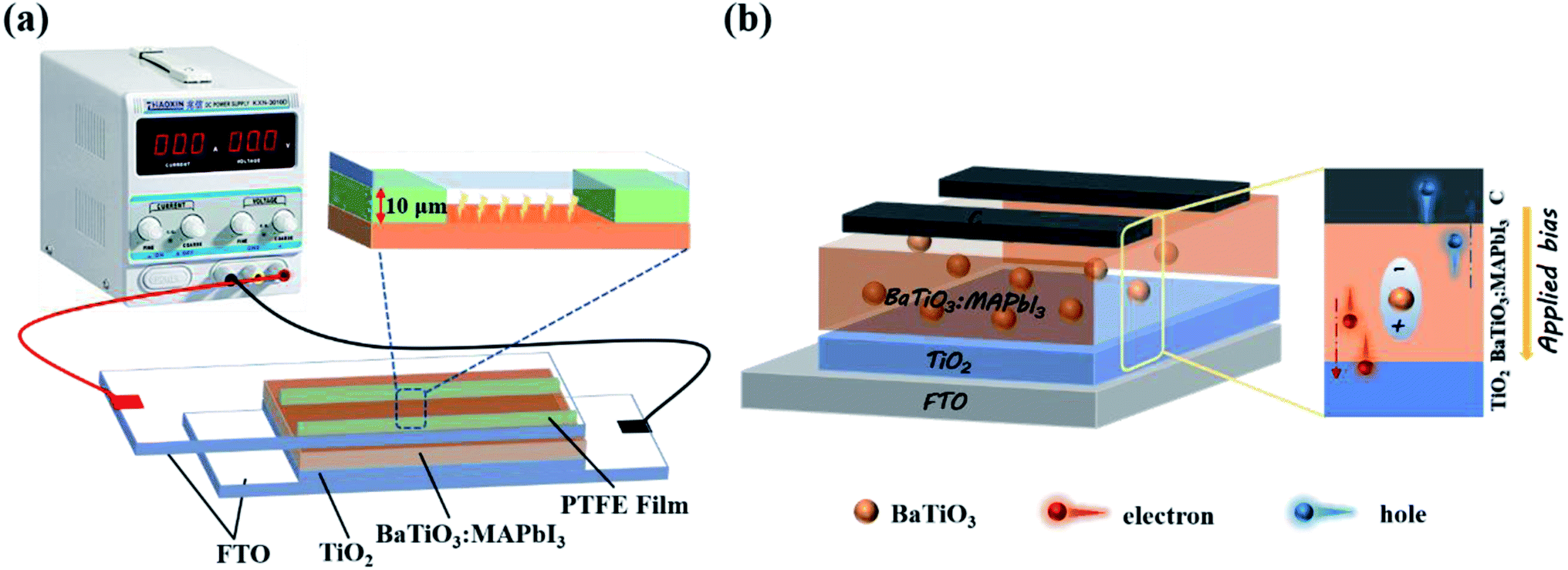 | ||
| Fig. 6 (a) A diagram of the thin film polarization device. (b) Polarization schematic diagram of the C-PSCs. | ||
 | ||
| Fig. 7 (a) J–V characteristic curves of the BaTiO3@MAPbI3-based C-PSCs treated with different voltage polarization. (b) Mott–Schottky curves; (c) steady-state PL spectra; and (d) voltage attenuation curves of the BaTiO3@MAPbI3-based C-PSCs before and after polarization treatment. | ||
| VOC (V) | JSC (mA cm−2) | FF (%) | PCE (%) | |
|---|---|---|---|---|
| Pristine | 0.888 | 13.47 | 47.10 | 5.64 |
| 0.5 V μm−1 | 0.989 | 15.72 | 55.66 | 8.65 |
| 1.0 V μm−1 | 1.005 | 15.59 | 56.40 | 8.83 |
| 2.0 V μm−1 | 0.940 | 14.92 | 50.57 | 7.09 |
Subsequently, the Mott–Schottky test was used to characterize the changes in the built-in electric field of the cell. Firstly, the depletion layer approximate model was used to fit the curve, and the formula is as follows.
| 1/C2 = (2/eεε0A2NA)(Vbi − V) | (3) |
| NA = 2/eεε0A2K | (4) |
 | (5) |
| NA (cm−3) | W (nm) | Vbi (V) | |
|---|---|---|---|
| Pristine | 0.888 | 13.47 | 47.10 |
| 0.5 V μm−1 | 0.989 | 15.72 | 55.66 |
| 1.0 V μm−1 | 1.005 | 15.59 | 56.40 |
| 2.0 V μm−1 | 0.940 | 14.92 | 50.57 |
The steady-state PL spectrogram, an important method, is used to investigate the carrier dynamics. The extraction rate of the carriers can be judged by comparing the degree of fluorescence quenching.29 Fig. 7(c) shows the steady-state PL spectra of the BaTiO3@MAPbI3-based C-PSCs before and after polarization treatment. The fluorescence intensity of the device after polarization treatment is significantly reduced, indicating that the carriers can be transported faster from the perovskite film to the electron transport layer. This process can avoid non-radiative recombination caused by the recombination center. The corresponding voltage decay curve is shown in Fig. 7(d). After the polarization treatment, the voltage decay rate of the C-PSCs decreases to induce a longer internal carrier life of the device, which is consistent with the PL spectrum result. The residual polarized electric field formed by the dipole provides the transmission power for the carriers, which is the key element to the life extension.
According to the principle of semiconductor heterojunction, we assume that the parallel resistance (Rsh) is infinite, the leakage current of the device can be ignored,30,31 and the I–V characteristic curve of a single heterojunction solar cell can be expressed as:32
| −dV/dJ = [(AKBT)/e](JSC − J)−1 + RS | (6) |
 | ||
| Fig. 8 (a) The relationship curve between −dV/dJ and (JSC − J)−1. (b) Relationship curve between ln(JSC − J) and (V + RSJ). (c) EIS curve. (d) Rrec at different bias of the BaTiO3@MAPbI3-based C-PSCs before and after polarization treatment. | ||
Finally, we further illustrate the principle of the performance caused by BaTiO3 nanoparticles doped C-PSCs light-absorbing layer, as shown in Fig. 9. The specific explanation is divided into two points. Firstly, we doped BaTiO3 nanoparticles with the C-PSCs light-absorbing layer, and the improvement in the cell performance is mainly caused by the increased quality of the light-absorbing layer film, leading to the improvement of the light absorption capacity. Furthermore, BaTiO3 and MAPbI3 are both regular octahedral structures. During the solvent volatilization and grain nucleation processes, BaTiO3 can be used as the site for grain nucleation and growth, and can reduce the holes in the film. Also, the increased size of the crystal grains can improve the film coverage and uniformity, and the defects inside the film are reduced to promote carrier transmission. On this basis, when a positive external electric field is applied to polarize the ferroelectric dipole, the electric dipoles will be aligned under the action of the external electric field to form a polarized electric field, which is opposite to the direction of the external electric field. After the external electric field is removed, there can still be a residual polarization electric field Eadd that is slightly smaller than the polarization electric field. Eadd and Ebi have the same direction, and the built-in electric field inside the film increases to Ebi′. The width of the depletion layer WETL is changed at the same time so that the carrier transmission ability is further improved, and the non-radiative recombination is suppressed. It is mainly due to the effective regulation of the ferroelectric material on the carrier transport, resulting in the significantly improved performance of the cell.
 | ||
| Fig. 9 Performance improvement schematic of the BaTiO3@MAPbI3-based C-PSCs. | ||
4 Conclusions
In summary, BaTiO3 was directly used as the additive in the perovskite precursor to prepare the BaTiO3@MAPbI3 composite film. The as-prepared perovskite film had better morphologies with the addition amount of 1.0 wt%. The crystallization performance of MAPbI3 was improved with increased grain size, and the residual PbI2 decreases to a certain degree, which effectively passivates the defects and reduces the defect state density. After the polarization treatment, the performance of the cell was significantly improved with the VOC of the cell reaching 1 V, and the PCE was 8.83%. It is proved that the realization of high-performance C-PSCs comes from the residual polarization electric field induced by the ferroelectric material BaTiO3. This can enhance the built-in electric field of the cell and increase the width of the depletion layer. Also, the increased driving force of carrier transport can promote the transport of the carriers and effectively suppress non-radiative recombination caused by the defects. The best device efficiency can reach 9.03% after optimization. This work mainly provides a possibility to design and develop optoelectronic devices with high-efficiency optoelectronic response behavior.Conflicts of interest
There are no conflicts to declare.Acknowledgements
This work was supported by the National Natural Science Foundation of China (No. 22005144, 51372115, 11575084), the Fundamental Research Funds for the Central Universities (No. NS2020038), and the Key Research and Development Projects of Jiangsu Province (No. BE2018091).References
- A. Kojima, K. Teshima, Y. Shirai and T. Miyasaka, Organometal halide perovskites as visible-light sensitizers for photovoltaic cells, J. Am. Chem. Soc., 2009, 131(17), 6050–6051 CrossRef CAS.
- NREL, Best Research-Cell Efficiency Chart, https://www.nrel.gov/pv/cell-efficiency.html, accessed 17 March 2021 Search PubMed.
- L. Boudad, M. Taibi, A. Belayachib and M. Abd-lefdilb, Structural, morphological, dielectric and optical properties of double perovskites RBaFeTiO6 (R = La, Eu), RSC Adv., 2021, 11, 40205–40215 RSC.
- X. Zheng, Y. Deng, B. Chen, H. Wei, X. Xiao, Y. Fang, Y. Lin, Z. Yu, Y. Liu, Q. Wang and J. Huang, Dual functions of crystallization control and defect passivation enabled by sulfonic zwitterions for stable and efficient perovskite solar cells, Adv. Mater., 2018, 30(52), 1803428 CrossRef.
- M. Kim, S. G. Motti, R. Sorrentino and A. Petrozza, Enhanced solar cell stability by hygroscopic polymer passivation of metal halide perovskite thin film, Energy Environ. Sci., 2018, 11(9), 2609–2619 RSC.
- N. Shrivastav, J. Madan, R. Pandey and A. E. Shalan, Investigations aimed at producing 33% efficient perovskite-silicon tandem solar cells through device simulations, RSC Adv., 2021, 11, 37366–37374 RSC.
- B. Chen, X. Zheng, M. Yang, Y. Zhou, S. Kundu, J. Shi, K. Zhu and S. Priya, Interface band structure engineering by ferroelectric polarization in perovskite solar cells, Nano Energy, 2015, 13, 582–591 CrossRef CAS.
- C. Zhang, Z. Wang, M. Li, Z. Liu, J. Yang, Y. Yang, X. Gao and H. Ma, Electric-field assisted perovskite crystallization for high-performance solar cells, J. Mater. Chem. A, 2018, 6, 1161–1170 RSC.
- A. Stroppa, C. Quarti, F. D. Angelis and S. Picozzi, Ferroelectric Polarization of CH3NH3PbI3: A Detailed Study Based on Density Functional Theory and Symmetry Mode Analysis, J. Phys. Chem. Lett., 2015, 6(12), 2223–2231 CrossRef CAS PubMed.
- F. Zheng, H. Takenaka, F. Wang, N. Z. Koocher and A. M. Rappe, First-principles calculation of the bulk photovoltaic effect in CH3NH3PbI3 and CH3NH3PbI3−xClx, J. Phys. Chem. Lett., 2015, 6(1), 31–37 CrossRef CAS PubMed.
- T. Wang, B. Daiber, J. M. Frost, S. A. Mann, E. C. Garnett, A. Walsh and B. Ehrler, Indirect to direct bandgap transition in methylammonium lead halide perovskite, Energy Environ. Sci., 2017, 10(2), 509–515 RSC.
- L. Leppert, S. E. Reyes-Lillo and J. B. Neaton, Electric field-and strain-induced Rashba effect in hybrid halide perovskites, J. Phys. Chem. Lett., 2016, 7(18), 3683–3689 CrossRef CAS PubMed.
- J. Beilsten-Edmands, G. E. Eperon, R. Johnson, R. D. Johnson, H. J. Snaith and P. G. Radaelli, Non-ferroelectric nature of the conductance hysteresis in CH3NH3PbI3 perovskite-based photovoltaic devices, Appl. Phys. Lett., 2015, 106(17), 173502 CrossRef.
- Z. Fan, J. Xiao, K. Sun, L. Chen, Y. Hu, J. Ouyang, K. P. Ong, K. Zeng and J. Wang, Ferroelectricity of CH3NH3PbI3 Perovskite, J. Phys. Chem. Lett., 2015, 6(7), 1155–1161 CrossRef CAS PubMed.
- Y. Yuan, T. J. Reece, P. Sharma, S. Poddar, S. Ducharme, A. Gruverman, Y. Yang and J. Huang, Efficiency enhancement in organic solar cells with ferroelectric polymers, Nat. Mater., 2011, 10(4), 296–302 CrossRef CAS PubMed.
- Z. Xiao, Q. Dong, P. Sharma, Y. Yuan, B. Mao, W. Tian, A. Gruverman and J. Huang, Synthesis and Application of Ferroelectric P(VDF-TrFE) Nanoparticles in Organic Photovoltaic Devices for High Efficiency, Adv. Energy Mater., 2013, 3(12), 1581–1588 CrossRef CAS.
- H. A. Moghaddam, M. R. Mohammadi and S. M. S. Reyhani, Improved photon to current conversion in nanostructured TiO2 dye-sensitized solar cells by incorporating cubic BaTiO3 particles deleting incident, Sol. Energy, 2016, 132, 1–14 CrossRef.
- K. Feng, X. Liu, D. Si, X. Tang, A. Xing, M. Osada and P. Xiao, Ferroelectric BaTiO3 dipole induced charge transfer enhancement in dye-sensitized solar cells, J. Power Sources, 2017, 350, 35–40 CrossRef CAS.
- M. Wang, H. Feng, C. Qian, J. He, J. Feng, Y. Cao, K. Yang, Z. Deng, Z. Yang, X. Yao, J. Zhou, S. Liu and X. Zeng, PbTiO3 as Electron-Selective Layer for High-Efficiency Perovskite Solar Cells: Enhanced Electron Extraction via Tunable Ferroelectric Polarization, Adv. Funct. Mater., 2019, 29(1), 1806427 CrossRef.
- A. Pérez-Tomas, H. Xie, Z. Wang, H. Kim, I. Shirley, S. Turren-Cruz, A. Morales-Melgares, B. Saliba, D. Tanenbaum, M. Saliba, S. M. Zakeeruddin, M. Gratzel, A. Hagfeldt and M. Lira-Cantu, PbZrTiO3 ferroelectric oxide as an electron extraction material for stable halide perovskite solar cells, Sustainable Energy Fuels, 2019, 3, 382–389 RSC.
- Y. Yang, Z. Liu, W. K. Ng, L. Zhang, H. Zhang, X. Meng, Y. Bai, S. Xiao, T. Zhang, C. Hu, K. Wong and S. Yang, An Ultrathin Ferroelectric Perovskite Oxide Layer for High-Performance Hole Transport Material Free Carbon Based Halide Perovskite Solar Cells, Adv. Funct. Mater., 2019, 29(1), 1806506 CrossRef.
- X. Xu, L. Xiao, J. Zhao, B. Pan, J. Li, W. Liao, R. Xiong and G. Zou, Molecular Ferroelectrics-Driven High-Performance Perovskite Solar Cells, Angew. Chem., Int. Ed., 2020, 59(45), 19974–19982 CrossRef CAS PubMed.
- C. Zhang, Z. Wang, S. Yuan, R. Wang, M. Li, M. F. Jimoh, L. Liao and Y. Yang, Polarized Ferroelectric Polymers for High-Performance Perovskite Solar Cells, Adv. Mater., 2019, 31(30), 1902222 CrossRef.
- H. Zarenezhad, M. Askari, M. Halali, N. Solati, T. Balkan and S. Kaya, Enhanced electron transport induced by a ferroelectric field in efficient halide perovskite solar cells, Sol. Energy Mater. Sol. Cells, 2020, 206, 110318 CrossRef CAS.
- P. Zhu, Y. Chen and J. Shi, Piezocatalytic Tumor Therapy by Ultrasound-Triggered and BaTiO3-Mediated Piezoelectricity, Adv. Mater., 2020, 32(29), 2001976 CrossRef CAS.
- H. Zhang, X. Wang, Z. Tian, C. Zhong and L. Li, Fabrication of Monodispersed 5-nm BaTiO3 Nanocrystals with Narrow Size Distribution via One-Step Solvothermal Route, J. Am. Ceram. Soc., 2011, 94(10), 3220–3222 CrossRef CAS.
- Q. Jiang, Z. Chu, P. Wang, X. Yang, H. Liu, Y. Wang, Z. Yin, J. Wu, X. Zhang and J. You, Planar-structure perovskite solar cells with efficiency beyond 21%, Adv. Mater., 2017, 29(46), 1703852 CrossRef.
- Z. Lu, S. Wang, H. Liu, F. Feng and W. Li, Improved efficiency of perovskite solar cells by the interfacial modification of the active layer, Nanomaterials, 2019, 9(2), 204 CrossRef CAS.
- A. Mei, Y. Sheng, Y. Ming, Y. Hu, Y. Rong, W. Zhang, S. Luo, G. Na, C. Tian, X. Hou, Y. Xiong, Z. Zhang, S. Liu, S. Uchida, T. Kim, Y. Yuan, L. Zhang, Y. Zhou and H. Han, Stabilizing Perovskite Solar Cells to IEC61215: 2016 Standards with over 9000-h Operational Tracking, Joule, 2020, 4(12), 2646–2660 CrossRef CAS.
- C. Liu, Z. Qiu, W. Meng, J. Chen, J. Qi, C. Dong and M. Wang, Effects of interfacial characteristics on photovoltaic performance in CH3NH3PbBr3-based bulk perovskite solar cells with core/shell nanoarray as electron transporter, Nano Energy, 2015, 12(1), 59–68 CrossRef CAS.
- Z. Jiang, Z. Xiao, Z. Tao, X. Zhang and S. Lin, A significant enhancement of bulk charge separation in photoelectrocatalysis by ferroelectric polarization induced in CdS/BaTiO3 nanowires, RSC Adv., 2021, 11, 26534–26545 RSC.
- S. S. Hegedus and W. N. Shafarman, Thin-film solar cells: device measurements and analysis, Prog. Photovoltaics, 2004, 12(2–3), 155–176 CAS.
| This journal is © The Royal Society of Chemistry 2022 |