
 Open Access Article
 This Open Access Article is licensed under a Creative Commons Attribution-Non Commercial 3.0 Unported Licence
Enhanced performance in uncooled n-CdSe/p-PbSe photovoltaic detectors by high-temperature chloride passivation
Yingmin Luoa,
Lance McDowellb,
Leisheng Sua,
Yun Liua,
Jijun Qiu *a and
Zhisheng Shi*b
*a and
Zhisheng Shi*b
aSchool of Microelectronics, Dalian University of Technology, Dalian, PR China 116024. E-mail: jjqiu@dlut.edu.cn
bSchool of Electrical and Computer Engineering, University of Oklahoma, Norman, Oklahoma 73019, USA. E-mail: shi@ou.edu
First published on 16th March 2022
Abstract
High-temperature chloride passivation (HTCP) was proposed to improve the crystalline quality and electrical properties of PbSe epitaxial films. The PL intensity of HTCP (111) PbSe epitaxial films exhibits a 14 times higher intensity than that of as-grown films, and a threefold increase in Hall mobility has been obtained after HTCP at 300 °C for 2 h. The improvement of optical and electrical properties is attributed to the high-temperature defect passivation induced by the HTCP process. The HTCP process of PbSe films was implemented in a CdSe/PbSe heterojunction PV detector, which exhibits a room temperature peak detectivity D* of 8.5 × 108 cm Hz1/2 W−1 in the mid-wavelength infrared region under blackbody radiation (227 °C), demonstrating potential applications in the fabrication of mid-infrared detectors and emitters.
1. Introduction
Lead selenide PbSe, being sensitive to mid-infrared wavelengths (MWIR, 3–5 μm) at room temperature, is a promising active material for optoelectronic devices, including high-sensitivity infrared (IR) photodetectors,1 IR-emitting diodes2 and lasers.3 It is widely accepted that an uncooled PbSe focal plane array (FPA) detector is the most cost-effective solution for multiple applications based on the detection of IR radiation.4 The utilization of the uncooled photoconductive (PC) PbSe detectors can be traced back to the mid-1960s, and still to this day offers some great advantages for military, commercial and medical applications due to their low-cost and comparable performance to their counterparts such as Hg1−xCdxTe (MCT) at room temperature.5–7 For example, Northrop-Grumman has developed a 320 × 240 staring PbSe FPA imaging system by modifying the standard chemical bath deposition (CBD) technology.8 In 2007, G. Vergara developed a new vapor phase deposition (VPD) PbSe technology and demonstrated for the first time a 128 × 128 MWIR PbSe detector monolithically integrated with the corresponding Si-CMOS circuitry.9However, its lower responsivity (D*) and smaller format have been putting PbSe FPA detectors at a disadvantage in competition with MCT for 30 years. The lower D* is mainly caused by a poor understanding of the complex physics involved in the photoconduction process in PbSe poly-crystals.10–12 The poorer uniformity in photo-response and shorter-term stability of photosensitive CBD PbSe films suffering from the oxygen or iodine sensitization process restrict the pixel size and format of arrays.13–15
Theoretically, these disadvantages of uncooled PbSe PC FPA detectors could be overcome by adopting a single-crystalline photovoltaic (PV) junction device configuration based on molecular beam epitaxy (MBE) technology, such as n-PbSe/p-PbSe homojunction and Pb/p-PbSe Schottky.16 MBE PbSe epitaxial films grown on silicon substrates have attracted more attention for large format FPA uncooled imaging applications, not only due to their large area uniformity and integration ability with Si wafer, but also extended photosensitive wavelength to long-IR range (8–12 μm) by Sn doping.17–20 Based on these advantages, Shi explored an n-CdS/p-PbSe heterojunction device configuration by combining the CBD and MBE technologies.17 However, the device performance is lower than both the theoretical limit and the PbSe PC detectors' performances, which is limited by high Shockley–Read Hall recombination associated with high dislocation density (>108 cm2) and high carrier concentration (typical 5 × 1017 cm−3) caused by large mismatch in lattice constant and coefficient of thermal expansion between lead-salt films and Si substrates.19
Many approaches have been carried out over the past several decades to eliminate or reduce those defects, including buffer layer and strained layer techniques,17 lateral growth, selected area growth,21,22 and ex situ annealing passivation techniques,23 such as oxygen (O2),24,25 calcium difluoride (CaF2),26 native sulfide27 and halide ions passivation.28,29 Among them, high-temperature (>300 °C) oxygen passivation annealing (HTOP) is a near-optimum solution for a PV detector performance breakthrough.23–25,30 Unfortunately, the HTOP process will destroy the surface flatness and uniformity of MBE-PbSe epitaxial films,24,25 limiting its application in the field of PV PbSe FPA detectors.
To avoid surface degradation, in this letter, a new post annealing process named as high-temperature chloride passivation (HTCP) was proposed to improve the crystalline quality of MBE PbSe films, leading to enhanced MBE PbSe PV detector performance. Subsequently, the HTCP-PbSe films were utilized to form PV detectors with n-type CdSe films, which were synthesized from thermal evaporation method. Comparing with n-CdS, it is believed that CdSe has a better potential to form a stronger heterojunction interface with PbSe due to the presence of the same anion (Se2−). By optimization of materials and process, a specific detectivity (D*) of 8.5 × 108 cm Hz1/2 W−1 was obtained under zero-bias photovoltaic mode.
2. Experiment
2.1 Fabrication of materials and assembly of PV detector
As a reference, ZnO films were deposited over MBE-PbSe epitaxial films via RF magnetron sputtering. A high purity (99.99%) ZnO target of 76.2 mm diameter was used for the deposition. The vacuum chamber was first evacuated to 5 × 10⁻⁴ Pa before the introduction of argon as the sputtering gas. The deposition was carried out at a pressure of 2.0 Pa in room temperature. The sputtering power was maintained at 200 W during deposition for 200 nm thickness.
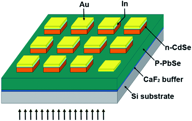 | ||
| Fig. 1 Schematic configuration of CdSe/HTCP-PbSe PV detector structure. | ||
A photoresist (AZ5241E) layer was coated onto CdSe/PbSe layer by spin-coating at 2500 rpm for 60 s followed by a soft bake for 90 s at 95 °C. Then, quadrate photoresist arrays with 200 × 200 μm were patterned by using an MJB3 mask aligner UV lithography (275 W) with an exposure time of 10 s, followed by a development time of 45 s. Subsequently, the patterned CdSe arrays on PbSe film were fabricated by 10 s wet chemical etching and acetone life off. The etchant consists of equal parts of 80% H3PO4, 29% HCl, and H2O. Next, electrode pattern was shaped by a second lithographic process, including a spin-coating at 2500 for 60 s, a soft bake at 95 °C for 90 s, UV exposure for 5 s, a hard bake at 120 °C for 90 s, a UV exposure for 50 s, and development for 60 s. Then, 50 nm indium (In) and 200 nm Au electrode were deposited in turn by employing thermal evaporation at room temperature for 10 min in 2 × 10⁻⁴ Pa. Finally, 200 × 200 μm Au/In electrodes on the CdSe arrays were obtained after lift-off in acetone solvent for 5 min.
3. Results and discussion
3.1 Theory
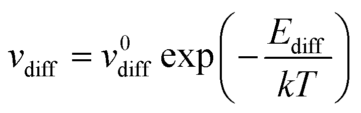
CdCl2 was selected to passivate the PbSe films based on the following four reasons. Firstly, the Cl substitutionary action on the Se sublattice leaves undisturbed the conduction band of PbSe that consists primarily of Pb orbitals.31 Secondly, it was confirmed that CdCl2 can effectively decrease the defect density of PbSe quantum dots as hybrid passivation scheme.32 Third, CdCl2 could be easily removed by low-cost wet-chemical etching method, and the etching does not cause any damage on the PbSe surface. Fourth, high temperature CdCl2 treatment is a key processing step identified in the late 1970s to drastically improve the solar to electric conversion efficiency of CdS/CdTe solar cells by passivating a large number of columnar grain boundaries and decreasing the intrinsic or native defects in CdS and CdTe layers.33–37The Cl diffusion and substitutionary in PbSe is assumed in a thermodynamic equilibration and is mediated by using a “concerted-exchange” process in which the dopant atom and one of its nearest-neighboring atoms swap places. Therefore, the activation temperatures could be calculated by a simple Arrhenius behavior:38
 | (1) |
Fig. 2 shows the theoretical diffusion temperature values in the light of above data, 789 °C for Cd and 254 °C for Cl. For a controllable diffusion rate, therefore, the heat-treatment temperature was limited below 400 °C, marked in yellow.
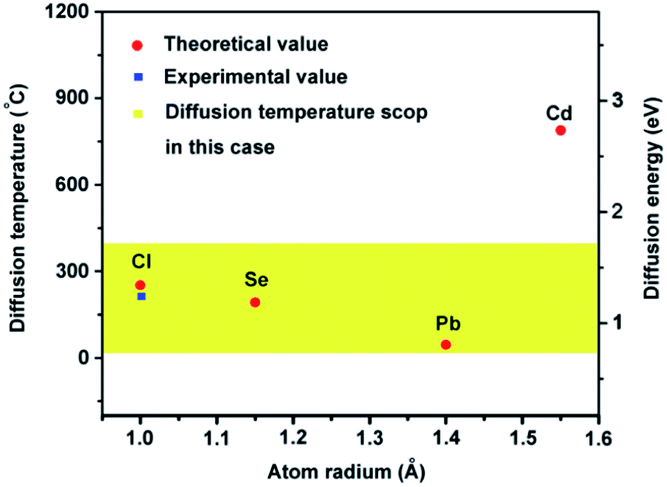 | ||
| Fig. 2 The theoretical and experimental diffusion temperatures for Cl, Se, Cd and Pb. | ||
3.2 Experimental results and discussion
Photoluminescence spectrum (PL) is considered to be an effective quality inspection technique by comparing the intensity of optical photoluminescence peaks. Fig. 3 shows the room temperature PL spectra of PbSe films that underwent HTCP at different annealing temperatures for an optimized time. In comparison, the RT PL spectrum for the as-grown MBE-PbSe film was given in Fig. 3a. It is obvious that the PL intensities were significantly enhanced as the annealing temperature increased, and maximum PL intensity was obtained at 300 °C (Fig. 3c), which is 14 times higher in comparison with the as-grown film. The subsequent experiments indicated that the enhanced intensity is due to the decreased defect density in PbSe films, which are attributed to the intrinsic-defect passivation caused by thermal annealing and the non-intrinsic defect passivation caused by Cl diffusion.24,25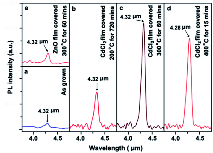 | ||
| Fig. 3 PL spectra of PbSe films with CdCl2 passivation at various temperature (a) as-grown MBE-PbSe film; (b) 200 °C; (c) 300 °C; (d) 400 °C; (e) reference sample. | ||
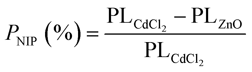
To calculate the contribution percentage from the Cl− non-intrinsic defect passivation, the PL of annealed PbSe epitaxial film covered with ZnO film was investigated, as shown in Fig. 3(e). The slight PL increase from ZnO coated MBE-PbSe film is only attributed to the thermal intrinsic defect passivation because for the following two reasons: (1) the Cl and O non-intrinsic compensation from the external environment were completely blocked by the dense ZnO film; (2) oxygen in ZnO unit cells couldn't produce any contribution to the non-intrinsic defect passivation due to a huge Zn–O bond strength of 150.6 KJ mol−1.42,43 Therefore, the contribution percentage from the non-intrinsic defect passivation PNIP (%):
 | (2) |
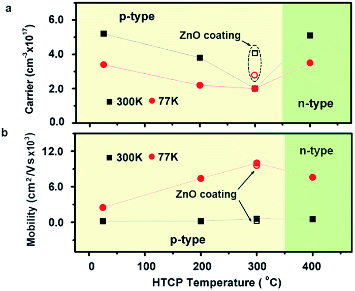
The carrier concentration and mobility as a function of CdCl2-treated temperature is shown in Fig. 4. The as-grown PbSe film was found to be p-type, and the carrier concentration was 3.4 × 1017 cm3 at 77 K and 5.2 × 1017 cm3 at room temperature (RT). After CdCl2 passivation, the carrier concentration decreased with increasing the annealing temperature, and reached minimum value of 2.0 × 1017 cm3 at 300 °C.
 | ||
| Fig. 4 Carrier concentration (a) and mobility (b) as a function of CdCl2 annealing temperature. | ||
Subsequently, the carrier concentration almost bounced back to the original value at 77 K and RT. Furthermore, the semiconductor type of PbSe transferred from p-type to n-type as annealing temperature increased up to 400 °C. The transformation of semiconductor type is attributed to the occurrence of the interstitial Cl− defects  and the selenium evaporation from PbSe triggered by high temperature. The decrease of carrier concentration resulted from the intrinsic defect, such as selenium vacancies
  passivated by Cl− diffusing into the PbSe and occupying
  , which is confirmed by the high carrier concentration of 4.1 × 1017 cm3 at 300 K and 2.9 × 1017 cm3 at 77 K of ZnO covered PbSe annealed at 300 °C for 1 h. Therefore, a decrease of nearly 65% in carrier concentration is attributed to the non-intrinsic defect passivation by Cl− diffusion. At the same time, the mobilities have a maximum of 600 cm2 V−1 s−1 at 300 K and 10
![[thin space (1/6-em)]](https://www.rsc.org/images/entities/char_2009.gif) 000 cm2 V−1 s−1 at 77 K after 300 °C HTCP, increasing 2 times and 3 times more than free-Cl− passivation samples, respectively. However, the mobility of CdCl2-passivated PbSe epitaxial film maintains the same value with ZnO-covered samples annealed at 300 °C, indicating that thermal intrinsic defect passivation plays a key role in promoting the mobility of MBE PbSe epitaxial films. This result was further confirmed by the fact that mobilities of ZnO covered PbSe film research 1000 at 300 K and 30000 cm2 v−1 s−1 at 77 K after annealing temperature was increased to 400 °C. In addition, there is no conducting type transition for ZnO-covered PbSe film until 450 °C, which further proves that lower conducting type transition temperature (400 °C) for CdCl2-passivated PbSe mainly is attributed to the interstitial Cl− defects
000 cm2 V−1 s−1 at 77 K after 300 °C HTCP, increasing 2 times and 3 times more than free-Cl− passivation samples, respectively. However, the mobility of CdCl2-passivated PbSe epitaxial film maintains the same value with ZnO-covered samples annealed at 300 °C, indicating that thermal intrinsic defect passivation plays a key role in promoting the mobility of MBE PbSe epitaxial films. This result was further confirmed by the fact that mobilities of ZnO covered PbSe film research 1000 at 300 K and 30000 cm2 v−1 s−1 at 77 K after annealing temperature was increased to 400 °C. In addition, there is no conducting type transition for ZnO-covered PbSe film until 450 °C, which further proves that lower conducting type transition temperature (400 °C) for CdCl2-passivated PbSe mainly is attributed to the interstitial Cl− defects  being n-type dopants.
Although O2 passivation can simply improve the quality of MBE-PbSe epitaxial films, the effective passivation temperature of >300 °C will severely damage the surface by forming an oxidation layer of PbSeO3 and selenium evaporation.25 The cross-view FESEM images of CdCl2-passiviated PbSe epitaxial films annealed at 300 °C is shown in Fig. 5. It is obvious that no surface damage was observed after high-temperature passivation and wet-chemical etching process. The smooth surface and the improved electrical properties provide the necessary morphological structure and electrical band structure to build high-performance PbSe PV detectors (Fig. 6).
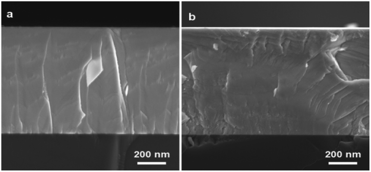 | ||
| Fig. 5 FESEM images of PbSe epitaxial films. (a) Without, and (b) with HTCP. | ||
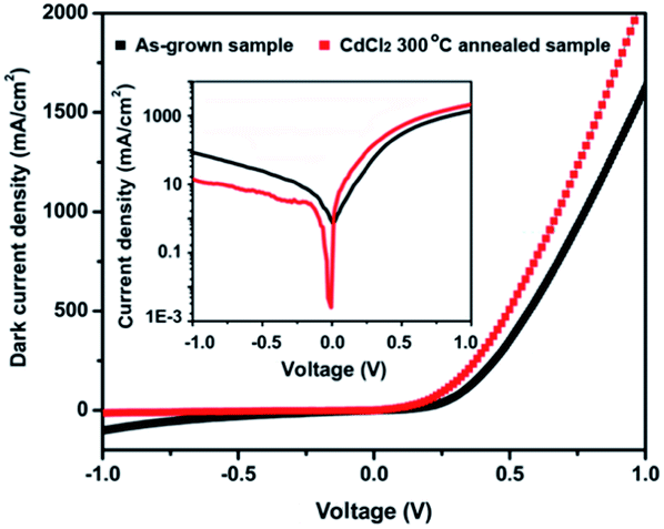 | ||
| Fig. 6 Dark current density–voltage (J–V) characteristics of CdSe/PbSe PV detectors with HTCP. | ||
Being a direct bandgap II–VI semiconductor with an electronic affinity of 4.85 ± 0.1 eV,44–46 CdSe combine with PbSe epitaxial film to form a type-II band alignment, which makes them suitable candidates for photovoltaics applications. An n-CdSe and p-PbSe p–n heterojunction PV detector was assembled to investigate the effects of HTCP on detector performance. The electrical characteristics of CdSe/PbSe photodiode without HTCP process has a 16.5 ON/OFF ratio, the reverse dark current of ∼72 mA cm−2 at −1 V, and an ideal factor (n) of ∼1.8. After the HTCP process, the reverse saturation current of the photodiode is 8 times lower than that free-HTCP photodiode at room temperature, and the ON/OFF ratio increases to 306. The decreased dark current of 9 mA cm−2 and the increased ON/OFF ratio are attributed to the improved crystal quality of PbSe epitaxial films after HTCP.
A relative response spectrum of the CdSe/PbSe PV detector was measured using a Fourier transform infrared spectrometer at room temperature. It is clear that the photosensitive band of the detector with HTCP ranges from 1.0 to 5.0 μm, and reaches a maximum at 3.8 μm. The cut-off wavelength of the photodiode is approximately 4.6 μm, which is larger than that of polycrystal PbSe photoconductive detectors fabricated from the standard CBD method, as shown in Fig. 7. It is 300 nm red-shift of the cutoff wavelength that makes CdSe/PbSe heterojunction PV detectors widely available for gas sensing.
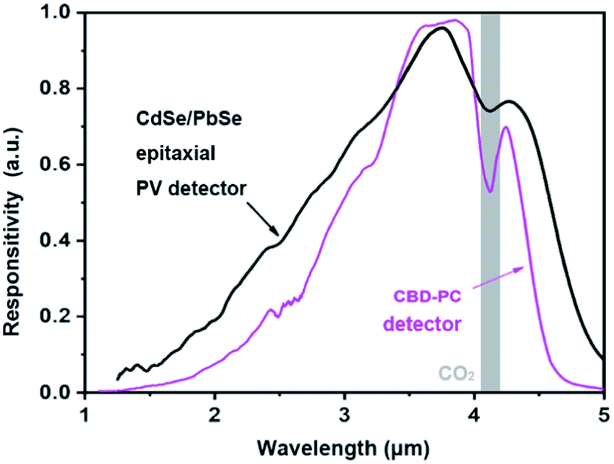 | ||
| Fig. 7 Room-temperature spectral response curves of the CdSe/PbSe PV detector and CBD-PbSe photoconductive detectors. | ||
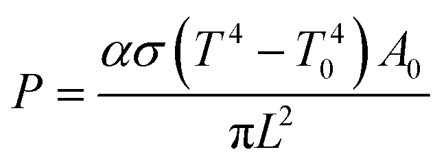
To further demonstrate the performance of the PV detector, photoelectric properties under blackbody illumination were subsequently investigated at room temperature. The blackbody detectivity (D*) of the device is calculated in the following way. The noise of PV detectors is primarily induced by 1/f noise, shot noise, and thermal noise. To ignore the 1/f noise which dominates at low frequency, the CdSe/PbSe PV detector was measured at a modulation frequency of 750 Hz. In addition, zero-bias photovoltaic mode was employed to minimize both the shot noise and the thermal noise. Hence, the D* could be calculated using the formula:
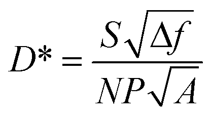
where α is modulation factor of chopper, σ is Stefan–Boltzmann constant, T is temperature of blackbody, T0 is room temperature, A0 is aperture area of blackbody and L is distance between blackbody and detectors. In our detection system the value of α is 0.45, T is 500 K, T0 is 300 K, A0 is 0.0127 cm2 and L is 20 cm. The measured room-temperature peak D* reaches 8.5 × 108 cm Hz1/2 W−1 in the MWIR region, which is more than 3 times performance of HTCP-free CdSe/PbSe detector. At the same time, the detectivity D* of CdSe/PbSe detectors is higher than that of CdS/PbSe PV detectors in our previous report, proving the feasibility of using CdSe/PbSe heterostructure for mid-IR detection at room temperature.
4. Conclusion
In conclusion, high-temperature chloride passivation (HTCP) was proposed to improve the crystalline quality and electrical properties of PbSe epitaxial films by thermal intrinsic defect passivation and Cl− non-intrinsic defect passivation. The PL intensity of the PbSe epitaxial film after undergoing HTCP at 300 °C exhibits a 14 times higher intensity than that of as-grown films. A threefold increase in Hall mobility was also obtained from HTCP at 300 °C. This simple HTCP process of PbSe films was implemented in the fabrication of CdSe/PbSe heterojunction PV detector, which demonstrated a significant device performance enhancement, with a peak detectivity D* of 8.5 × 108 cm Hz1/2 W−1 at 3.8 μm under zero-bias photovoltaic mode. HTCP shows a potential application in the fabrication of mid-infrared detectors and emitters.Author contributions
J. Q. conceived the presented idea, carried out the materials growth, fabricated the detectors and performed the characterization. Y. L and L. M analysed the data and wrote the manuscript with support from L. S., Y. L. Both J. Q. and Z. S. contributed to the final version of the manuscript. Z. S. supervised the findings of this work.Conflicts of interest
There are no conflicts to declare.Acknowledgements
All conceptual and experimental work were completed at the University of Oklahoma, which was supported by the US DARPA WIRED program through Northrop Grumman, and US army research office (ARO) under contract no. W911NF-18-1-0418. The manuscript was completed at Dalian University of Technology, China. The writing of the manuscript was funded by the Dalian Science and Technology Innovation Fund (2020JJ26GX022) and Fundamental Research Funds for the Central Universities (Grant No. DUT19RC (3)032).Notes and references
- S. Roa, M. Sandoval and M. Sirena, Mater. Chem. Phys., 2021, 264, 124479 CrossRef CAS.
- J. Zhang, X. Liu, P. Jiang, H. Chen, Y. Wang, J. Ma, R. Zhang, F. Yang, M. Wang, J. Zhang and G. Tu, Nano Energy, 2019, 66, 104142 CrossRef CAS.
- C. L. Felix, W. W. Bewley, I. Vurgaftman, J. R. Lindle, J. R. Meyer, H. Z. Wu, G. Xu, S. Khosravani and Z. Shi, Appl. Phys. Lett., 2001, 78, 3770–3772 CrossRef CAS.
- M. Kastek, T. Piątkowski, H. Polakowski, J. Barela, K. Firmanty, P. Trzaskawka, G. Vergara, R. Linares, R. Gutierrez, C. Fernandez and M. T. Montojo, Proc. SPIE, 2014, 9074, 90740A CrossRef.
- Y. X. Ren, T. J. Dai, W. B. Luo and X. Z. Liu, Vacuum, 2018, 149, 190–194 CrossRef CAS.
- J. Qiu, B. Weng, Z. Yuan and Z. Shi, J. Appl. Phys., 2013, 113, 103102 CrossRef.
- F. Briones, D. Golmayo and C. Ortiz, Thin Solid Films, 1981, 78, 385–395 CrossRef CAS.
- T. Beystrum, R. Himoto, N. Jacksen and M. Sutton, Proc. SPIE, 2004, 5406, 287–294 CrossRef.
- G. Vergara, L. J. Gómez, V. Villamayor, M. Álvarez, M. C. Torquemada, M. T. Rodrigo, M. Verdú, F. J. Sánchez, R. M. Almazán, J. Plaza, P. Rodriguez, I. Catalán, R. Gutierrez, M. T. Montojo, F. Serra-Graells, J. M. Margarit and L. Terés, Proc. SPIE, 2007, 6542, 654220–654229 CrossRef.
- C. Marcott, R. C. Reeder, J. A. Sweat, D. D. Panzer and D. L. Wetzel, Vib. Spectrosc., 1999, 19, 123–129 CrossRef CAS.
- V. Kasiyan, Z. Dashevsky, C. Minna Schwarz, M. Shatkhin, E. Flitsiyan, L. Chernyak and D. Khokhlov, J. Appl. Phys., 2012, 112, 86101 CrossRef.
- R. L. Petritz, Phys. Rev., 1956, 104, 1508–1516 CrossRef CAS.
- R. Ahmed and M. C. Gupta, Opt. Lasers Eng., 2020, 134, 106299 CrossRef.
- M. Jang, P. M. Litwin, S. Yoo, S. J. McDonnell, N. K. Dhar and M. C. Gupta, J. Appl. Phys., 2019, 126, 105701 CrossRef.
- P. Kumar, M. Pfeffer, E. Schweda, O. Eibl, J. Qiu and Z. Shi, J. Alloys Compd., 2017, 724, 316–326 CrossRef CAS.
- H. Zogg, A. Fach, J. John, J. Masek, P. Mueller, C. Paglino and S. Blunier, Opt. Eng., 1995, 34, 1964–1969 CrossRef.
- B. Weng, J. Qiu, L. Zhao, C. Chang and Z. Shi, Appl. Phys. Lett., 2014, 104, 121111 CrossRef.
- M. T. Rodrigo, J. Diezhandino, G. Vergara, G. Perez, M. C. Torquemada, F. J. Sanchez, V. Villamayor, R. Almazan, M. Verdu, I. Genova, P. Rodriguez, L. J. Gomez, I. Catalan, J. Plaza and M. T. Montojo, Detectors and Associated Signal Processing, 2004, vol. 5251, pp. 97–102 Search PubMed.
- P. Muì Ller, A. Fach, J. John, A. N. Tiwari, H. Zogg and G. Kostorz, J. Appl. Phys., 1996, 79, 1911–1916 CrossRef.
- X. Shi, Q. Phan, B. Weng, L. L. McDowell, J. Qiu, Z. Cai and Z. Shi, Detection, 2018, 06, 1–16 CrossRef CAS.
- A. Osherov and Y. Golan, MRS Bull., 2010, 35, 790–796 CrossRef CAS.
- J. Chen, Q. Ma, X. Wu, L. Li, J. Liu and H. Zhang, Nano-Micro Lett., 2019, 11, 86 CrossRef CAS.
- X. Sun, K. Gao, X. Pang, H. Yang and A. A. Volinsky, J. Mater. Sci.: Mater. Electron., 2016, 27, 1670–1678 CrossRef CAS.
- F. Zhao, S. Mukherjee, J. Ma, D. Li, S. L. Elizondo and Z. Shi, Appl. Phys. Lett., 2008, 92, 211110 CrossRef.
- F. Zhao, J. Ma, D. Li, S. Mukherjee, G. Bi and Z. Shi, J. Electron. Mater., 2009, 38, 1661–1665 CrossRef CAS.
- S. Mukherjee, D. Li, G. Bi, J. Ma, S. L. Elizondo, A. Gautam and Z. Shi, Microelectron. Eng., 2011, 88, 314–317 CrossRef CAS.
- C. Gautier, G. Breton, M. Nouaoura, M. Cambon, S. Charar and M. Averous, J. Electrochem. Soc., 1998, 145, 512–517 CrossRef CAS.
- A. C. Bouley, H. R. Riedl, J. D. Jensen and S. R. Jost, US Pat., US4442446A, 1984 Search PubMed.
- M. Drinkwine, J. Rozenbergs, S. Jost and A. Amith, Proc. SPIE-Int. Soc. Opt. Eng., 1981, 285, 36–43 CrossRef CAS.
- K. Shi, Y. Liu, Y. Luo, J. Bian and J. Qiu, RSC Adv., 2021, 11, 36895–36900 RSC.
- J. Androulakis, D. Y. Chung, X. Su, Z. Li, C. Uher, T. C. Hasapis, E. Hatzikraniotis, K. M. Paraskevopoulos and M. G. Kanatzidis, Phys. Rev. B: Condens. Matter Mater. Phys., 2011, 84, 564–576 CrossRef.
- A. H. Ip, S. M. Thon, S. Hoogland, O. Voznyy, D. Zhitomirsky, R. Debnath, L. Levina, L. R. Rollny, G. H. Carey, A. Fischer, K. W. Kemp, I. J. Kramer, Z. Ning, A. J. Labelle, K. W. Chou, A. Amassian and E. H. Sargent, Nat. Nanotechnol., 2012, 7, 577–582 CrossRef CAS.
- W. K. Metzger, D. Albin, M. J. Romero, P. Dippo and M. Young, J. Appl. Phys., 2006, 99, 103703 CrossRef.
- A. R. Marshall, M. R. Young, A. J. Nozik, M. C. Beard and J. M. Luther, J. Phys. Chem. Lett., 2015, 6, 2892–2899 CrossRef CAS.
- E. Regalado-Pérez, M. G. Reyes-Banda and X. Mathew, Thin Solid Films, 2015, 582, 134–138 CrossRef.
- R. W. Crisp, D. M. Kroupa, A. R. Marshall, E. M. Miller, J. Zhang, M. C. Beard and J. M. Luther, Sci. Rep., 2015, 5, 9945 CrossRef CAS PubMed.
- M. J. Kim, J. J. Lee, S. H. Lee and S. H. Sohn, Sol. Energy Mater. Sol. Cells, 2013, 109, 209–214 CrossRef CAS.
- E. Ko, M. M. G. Alemany and J. R. Chelikowsky, J. Chem. Phys., 2004, 121, 942–945 CrossRef CAS PubMed.
- S. C. Erwin, Phys. Rev. B: Condens. Matter Mater. Phys., 2010, 81, 235433 CrossRef.
- F. D. Ott, L. L. Spiegel, D. J. Norris and S. C. Erwin, Phys. Rev. Lett., 2014, 113, 156803 CrossRef PubMed.
- A. Kutana and S. C. Erwin, Phys. Rev. B: Condens. Matter Mater. Phys., 2011, 83, 235419 CrossRef.
- T. Honma, Y. Benino, T. Komatsu, R. Sato and V. Dimitrov, Phys. Chem. Glasses, 2002, 43, 32–40 CAS.
- K. SUN, J. Am. Ceram. Soc., 1947, 30, 277–281 CrossRef CAS.
- V. Stevanovi, S. Lany, D. S. Ginley, W. Tumas and A. Zunger, Phys. Chem. Chem. Phys., 2014, 16, 3706–3714 RSC.
- S. Kasap and P. Capper, Springer handbook of electronic and photonic materials, 2nd edn, 2017 Search PubMed.
- Ya. I. Lepikh, I. A. Ivanchenko and L. M. Budiyanskaya, Semicond. Phys., Quantum Electron. Optoelectron., 2014, 17, 408–411 CrossRef CAS.
| This journal is © The Royal Society of Chemistry 2022 |