
 Open Access Article
 This Open Access Article is licensed under a Creative Commons Attribution-Non Commercial 3.0 Unported Licence
RbSnX3 (X = Cl, Br, I): promising lead-free metal halide perovskites for photovoltaics and optoelectronics
Md. Habibur Rahman *a,
Md. Jubairb,
Md. Zahidur Rahamanc,
Md. Shamim Ahasand,
Kostya (Ken) Ostrikove and
Md Roknuzzaman*ef
*a,
Md. Jubairb,
Md. Zahidur Rahamanc,
Md. Shamim Ahasand,
Kostya (Ken) Ostrikove and
Md Roknuzzaman*ef
aDepartment of Mechanical Engineering, Bangladesh University of Engineering and Technology, Dhaka 1000, Bangladesh. E-mail: imd.habiburrahman@gmail.com
bDepartment of Physics, Rajshahi University of Engineering and Technology, Rajshahi 6204, Bangladesh
cSchool of Materials Science and Engineering, University of New South Wales, Sydney, NSW 2052, Australia
dDepartment of Physics, University of Rajshahi, Rajshahi 6205, Bangladesh
eSchool of Chemistry and Physics and QUT Centre for Materials Science, Queensland University of Technology (QUT), Brisbane, QLD 4000, Australia. E-mail: roknphy@gmail.com
fSchool of Physics, University of New South Wales, Sydney, NSW 2052, Australia
First published on 7th March 2022
Abstract
Lead (Pb) free metal halide perovskites by atomistic design are of strong interest to photovoltaics and optoelectronics industries because of the pressing need to resolve Pb-related toxicity and instability challenges. In this study, structural, mechanical, electronic, and optical properties of Pb-free RbSnX3 (X = Cl, Br, I) perovskites have been evaluated by using ab initio density functional theory (DFT) calculations. The computed elastic constants suggest that the Rb-based halide perovskites are mechanically stable and highly ductile, making them suitable as flexible thin films in optoelectronic devices. Besides, the investigated electronic band structures reveal that the RbSnX3 compounds are direct bandgap semiconductors, suitable for photovoltaic and optoelectronic applications. Furthermore, several optical parameters such as dielectric functions, reflectivity, photon absorptions, refractive index, optical conductivity, and loss functions have been investigated and the results predict the excellent optoelectronic efficiency of RbSnX3. Also, the computed mechanical and optical properties of RbSnX3 (X = Cl, Br, I) have been compared with the previously studied CsBX3 (B = Ge, Sn, Pb; X = Cl, Br, I) phases, revealing that the Rb-based perovskites are extremely ductile and possess excellent light absorption and optical conductivity compared to the Cs-based perovskites. Importantly, RbSnI3 shows superior ductility, absorption coefficient, and optical conductivity compared to the CsBX3 (B = Ge, Sn, Pb; X = Cl, Br, I) perovskites. Superior absorption at the ultraviolet region of RbSnI3 holds great promise of this perovskite to be used in next-generation ultraviolet photodetectors.
1. Introduction
Halide perovskites presented by the general formula ABX3 (where, A = inorganic or organic cation, B = metal cation, and X = halogen anion) have outstanding prospects for industrial applications due to natural abundance and low cost.1 Furthermore, the materials can be deposited as thin films and other essential forms such as quantum dots, nanocrystals, nanowires, nanorods, nanoparticles, and millimeter-scale crystals, which are actively pursued by a broad range of devices.1–4 Therefore, it is expected that the technology associated with perovskites can be competitive with the conventional Si-based technology.3 On the other hand, halide perovskites represent an emerging class of materials due to a combination of highly desired physical properties such as a tunable direct bandgap, high photonic absorption along with a wide absorption spectrum, low carrier effective masses, and high charge carrier mobility with long-range charge diffusion as well as high optical conductivity and photoconductivity.2,3 Because of these exceptional optoelectronic properties, this group of semiconductors have the potential to be employed in a wide range of device applications such as photovoltaic cells, color light-emitting diodes (LEDs), field-effect transistors (FET), lasers, light-emitting electrochemical cells (LECs), photocatalysts, X-ray detectors, photodetectors, photoluminescence (PL), electroluminescence (EL), and solar-to-fuel conversion devices.2Temperature-dependent structural phase transitions are very common in halide perovskites.5–7 Different perovskites have been found in multiple crystallographic phases at different temperatures and the common phases are cubic, tetragonal, and orthorhombic.6,7 However, the cubic phase is the most common phase among the perovskite materials.6 Moreover, the cubic perovskite phase is widely accepted as a room-temperature phase which is generally found at a higher temperature compared to other existing phases, therefore the cubic phase is also called the high-temperature phase.5 Although perovskites have been well recognized for many years,8 they have become popular in the science community after the discovery of perovskite solar cells in 2009.9 In particular, the demand for halide perovskites has been boosted recently due to their very rapidly rising power conversion efficiency (PCE) in photovoltaic cells, because the PCE of the photovoltaic cells based on perovskites has climbed from 3.8% (2009)9 to 25.2% (2019)10 within 10 years. Generally, good light-absorbing material is also a good candidate as a light emitter and the concept further inspires the scientists to search for other possible applications of inorganic and hybrid perovskites. Research suggests that perovskites can also be utilized in other optoelectronic devices in addition to their most common application in photovoltaic cells.11 Because of their high photoluminescence quantum efficiencies, it has been found that the perovskites are suitable in light-emitting diodes (LEDs).12 Additionally, the bandgap of the perovskites can be easily adjusted within the energy range of visible light spectra by changing the halogen content which makes these materials potentially suitable for color light-emitting diodes.13 Importantly, research also suggests that the mixed halide perovskite materials showed a clearly semiconducting behavior making them suitable for optically pumped vertical-cavity surface-emitting lasers (VCSELs).11
Although a substantial amount of research work has been reported recently, the halide perovskites are still under development as some difficulties are yet to be resolved. For the commercial applications of perovskites, low cost, high efficiency, and especially long-term stability are required.14 To date, the most promising perovskites are based on MAPbX3 (X = Cl, Br, I) and they contain organic MA which causes the materials to be decomposed upon exposure to air or moisture. As a result, these perovskites do not show sufficient stability.15 In addition, a low dielectric constant is observed in Pb-based hybrid perovskites MAPbX3 (X = I, Br, Cl) compared to that in silicon. This low dielectric constant of hybrid perovskites is a disadvantage for photovoltaic applications as the low dielectric constant causes an increase in the recombination rate of charge carriers which in turn affects the device photovoltaic performance.8 Besides, the materials contain lead (Pb) constituent and it is considered as a toxic element that can cause severe damage to the environment.8 The best possible strategy to avoid toxicity is the replacement of Pb with non-toxic elements.16 Therefore, it is extremely vital to obtain Pb-free stable perovskites for the further development of the highly promising perovskites-based technology.
Interestingly, the potentiality of inorganic perovskites in device applications cannot be ignored as the materials have a similar crystallographic structure and show similar physical properties as hybrid perovskites.2 Furthermore, the inorganic perovskites are expected to be more stable than their hybrid counterparts.4 Therefore, Pb-free inorganic metal halide perovskites could be a game changer in perovskite based photovoltaics and optoelectronics. From this perspective, a significant amount of research works have been reported on Pb-free inorganic metal halide perovskites.2–4 For instance, mechanical, electrical, and optical properties of CsBX3 (B = Ge, Sn, Pb; X = Cl, Br, I) have been thoroughly analyzed.4 However, the Rb-based metal halide perovskites have not attracted the attention they merit. Hence, we consider Rb-based perovskites RbSnX3 (X = Cl, Br, I) to investigate their physical properties of interest for photovoltaics and optoelectronics. Like other perovskites, our considered perovskites have been found in different phases.7,17,18 However, we focus on the cubic phase,6 as the perovskites with promising photovoltaic and optoelectronic properties are mostly cubic.2–4 Nevertheless, studying the cubic phase of RbSnX3 (X = Cl, Br, I) can provide a great opportunity to compare our results with other perovskites and it will lead to obtaining optimum properties for photovoltaics and optoelectronics. Limited relevant analyses have been previously described in the literature.5–7,19–24 Specifically, results on phase change and phase stability of RbSnX3 (X = Cl, Br, I) have been published by several groups.5–7,19–21 In addition, the electronic bandgap of the considered perovskites has been reported either for a group of compounds or individual compounds.20–24 A recent study24 reports on the structural, electronic as well as optical constants of RbSnCl3 and RbSnBr3. However, the detailed optical properties of these materials are yet to be explored. To the best of our knowledge, the mechanical properties of the RbSnX3 (X = Cl, Br, I) perovskites and the optical properties of RbSnI3 have not been studied yet. Therefore, here we investigate the various physical properties of Pb-free metal halide cubic perovskites RbSnX3 (X = Cl, Br, I), primarily focusing on the unexplored mechanical and partially explored optical properties. Also, a thorough comparison with Cs-based perovskites has been carried out and it shows that the considered Rb-based perovskites are promising for photovoltaic and optoelectronic applications.
2. Theoretical approach
The Density Functional Theory (DFT)-based25,26 plane-wave pseudopotential methodology implemented in the CASTEP27 code is employed to accomplish the theoretical calculations. It is acknowledged that the van der Waals (vdW) correction scheme with standard DFT is also a popular theoretical approach and is basically used to account for the molecule/surface long-range interactions, useful in studying the adsorption of molecules in the surface, and so on.28–30 However, the present work reports the structural and optoelectronic features of bulk metal halide perovskites, where atoms are bonded by covalent bonding and therefore the vdW correction may not necessary. Overall, the standard DFT is widely used to investigate the properties of bulk materials like halide perovskites as evident in the literature.4,5 In this work, Generalized Gradient Approximation (GGA) with the Perdew–Burke–Ernzerhof (PBE)31 exchange-correlation functional is utilized for approximating the exchange-correlation energy. A plane wave cutoff energy of 600 eV is employed to expand the wave function, and the Monkhorst–Pack scheme32 is utilized to encompass the k-point sampling of the Brillouin zone. The geometry optimization as well as other calculations are performed by using 16 × 16 × 16 k-points. Certainly, the number of k-points is sufficient for the excellent convergence of all the studied compounds. Ultrasoft pseudopotential33 is applied for defining the electron–ion interaction. The geometry optimization is achieved by the Broyden–Fletcher–Goldfarb–Shanno (BFGS)34 relaxation scheme. A convergence threshold of 5 × 10⁻⁶ eV per atom, 0.01 eV Å−1, 0.02 GPa, and 5 × 10⁻⁴ Å are used for the total energy, maximum force, maximum stress, and maximum displacements, respectively for the optimization of the crystal geometry.3. Results and discussion
3.1. Structural properties
It is essential to know the structural stability of a hypothetical compound before evaluating its merit for practical applications. It has been reported several times in the literature that our considered perovskites RbSnX3 (X = Cl, Br) are expected to be stable in the cubic structure.5–7 The crystal structure of the conventional unit cells of the considered cubic perovskites is shown in Fig. 1. The calculated lattice parameter for the fully relaxed optimized conventional unit cell of cubic RbSnX3 (X = Cl, Br, I) is presented in Table 1. The estimated optimized lattice parameters have been observed to be in excellent agreement with the available reported data,23,24 as compared in Table 1. Moreover, the first principle computation implies that the structural features of RbSnX3 (X = Cl, Br, I) might be changed on a routine basis when atoms are replaced by analogous halogen atoms. Furthermore, the swapping of Cl for Br and I result in an increase in structural parameters. Since the changes in structural parameters are predicted to modulate the elastic and optoelectronic properties, this periodic shift in structural parameters may be utilized to adjust the optical as well as the electronic properties of RbSnX3 (X = Cl, Br, I).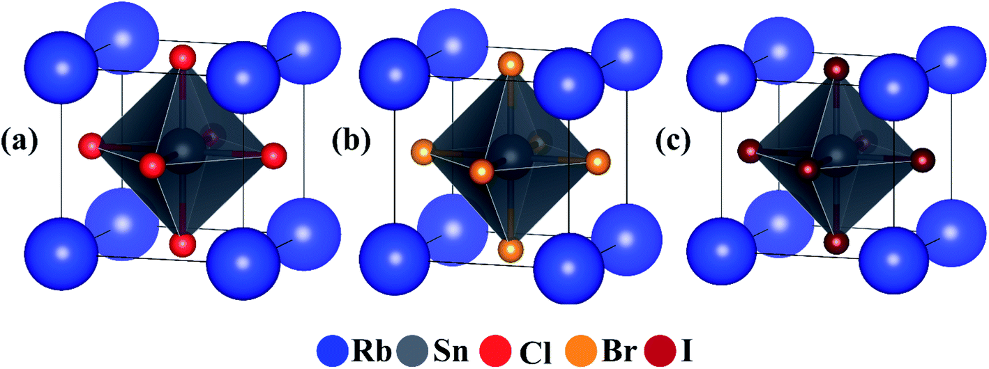 | ||
| Fig. 1 Crystal structure of cubic perovskites. Conventional unit cell of cubic Rb-based perovskites; (a) RbSnCl3, (b) RbSnBr3 and (c) RbSnI3. | ||
3.2. Mechanical properties
It is vital to calculate the intrinsic mechanical characteristics such as shear modulus (G), bulk modulus (B), Young's modulus (Y), Poisson ratio (ν), softness and failure mode (ductile or brittle) of a material considered for practical industrial implementations.4,8 The mechanical characteristics of RbSnX3 (X = Cl, Br, I), however, are still unexplored. Herein, the elastic constants of the selected halide perovskites are calculated by using the finite strain theory,35 which is incorporated in the CASTEP code and is widely used to compute the elastic characteristics of a wide range of materials, including semiconductors.8 According to this theory, a system is subjected to a series of homogenous deformations, and the resulting stress is quantified.8,14 The elastic constants are then determined using the formula σi = Cijεj, which relates the applied strain to the generated stress.8,14 The proportionality constants, Cij, are the elastic constants in this case.8,14 Afterward, the Voigt, Reuss, and Hill techniques36 have been used to obtain the elastic moduli such as bulk modulus (B) and shear modulus (G) of the polycrystalline sample from the single crystal elastic constants. For a cubic crystal, the bulk modulus can be obtained directly from the elastic constants by the formula:37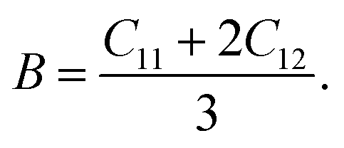
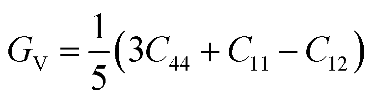
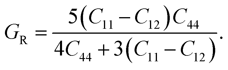
On the other hand, the equations for shear modulus according to Voigt (GV) and Reuss (GR) approximations can be written for the cubic crystal as:37
Finally, the shear modulus (G) can be estimated by using the Hill approximation36 as:
Also, using the formulas,  Young's modulus (Y) and Poisson ratio (ν) have been determined, respectively.4,14
Table 2 represents the estimated elastic constants and modulus from the DFT calculations. The mechanical stability of a crystal can be predicted by examining the elastic constants. It is worth mentioning that the cubic crystal has three independent elastic constants which are C11, C12, and C44, also the well-known Born stability requirements for this crystal are C11 − C12 > 0, C11 + 2C12 > 0, and C44 > 0.38 Based on these criteria, the studied RbSnX3 (X = Cl, Br, I) has been confirmed to be mechanically stable. Note that B is a measure of the volumetric stiffness of a particular compound, and is specified as its resistance to volume deformation.8,14 The predicted B of the RbSnX3 (X = Cl, Br, I) varies from 23.02 GPa (RbSnCl3) to 17.07 GPa (RbSnI3). Furthermore, G is a measure of plastic deformation of a material, in other words, shape change; a lower value of G implies that the compound is less stiff and has poor resistance to shape change.8 The G of the Pb free halide perovskites in this study varies from 6.70 GPa (RbSnI3) to 9.36 GPa (RbSnCl3). Importantly, the low B and G of RbSnX3 (X = Cl, Br, I) imply that they are flexible.14 As a result, these Pb-free inorganic metal halide perovskites may be easily transformed into thin films, rendering them suitable for optoelectronic applications such as photodetectors and solar devices.4,8 It is worth mentioning that the replacement of Cl and Br by I reduces the mechanical resistance in RbSnX3 (X = Cl, Br, I); which can be ascribed to the low bonding strength in the RbSnI3 crystal owing to the high atomic size, and ionic radius of I (140 pm and 206 pm) compared to that of Br (115 pm and 182 pm) and Cl (110 pm and 181 pm).39 In fact, the huge atomic size and ionic radius of the I imposes a notable amount of pressure within the crystal, resulting in a decreased bonding strength.39
| Compounds | C11 | C12 | C44 | B | G | Y | B/G | ν |
|---|---|---|---|---|---|---|---|---|
| a Ref. 4. | ||||||||
| RbSnCl3 | 52.23 | 8.42 | 4.85 | 23.02 | 9.36 | 24.74 | 2.45 | 0.32 |
| RbSnBr3 | 45.68 | 6.67 | 4.29 | 19.67 | 8.31 | 21.86 | 2.36 | 0.31 |
| RbSnI3 | 36.27 | 7.47 | 3.79 | 17.07 | 6.70 | 17.78 | 2.54 | 0.32 |
| CsPbI3a | 34.23 | 4.46 | 3.24 | 14.38 | 6.30 | 14.49 | 2.28 | 0.32 |
| CsPbBr3a | 42.32 | 6.51 | 4.24 | 18.45 | 7.90 | 20.74 | 2.33 | 0.31 |
| CsPbCl3a | 48.97 | 7.83 | 5.08 | 21.54 | 9.27 | 24.32 | 2.32 | 0.31 |
| CsSnI3a | 21.34 | 1.22 | 5.74 | 6.30 | 7.55 | 16.18 | 0.83 | 0.07 |
| CsSnBr3a | 43.89 | 6.69 | 5.21 | 19.09 | 8.94 | 23.19 | 2.13 | 0.30 |
| CsSnCl3a | 50.66 | 8.71 | 6.01 | 22.70 | 10.20 | 26.61 | 2.22 | 0.30 |
| CsGeI3a | 40.32 | 8.18 | 8.87 | 18.89 | 11.28 | 28.32 | 1.67 | 0.25 |
| CsGeBr3a | 48.08 | 10.82 | 10.07 | 23.24 | 12.92 | 32.70 | 1.8 | 0.27 |
| CsGeCl3a | 54.93 | 13.08 | 12 | 27.03 | 15.02 | 38.02 | 1.80 | 0.27 |
The B/G ratio, also recognized as Pugh's ratio, is used to identify the failure mechanism of a particular material, i.e., ductility or brittleness.40 The Pugh's ratio has a critical value of 1.75 to differentiate brittle from ductile materials, whereas the ν does have a critical value of 0.26 to separate brittle from ductile materials.40 If the Pugh's ratio is larger than 1.75 and the ν is greater than 0.26, the material is regarded as ductile; otherwise, it is referred to as brittle.40 Additionally, the greater Pugh's and ν values indicate excellent ductility, rendering the material more attractive for optoelectronic devices.4,8 All the Pb free halide RbSnX3 (X = Cl, Br, I) perovskites in this assessment are found to be highly ductile in nature, according to the criteria. The more ductile materials are more appropriate for optoelectronic devices.4,41 It is reported that Pb-based perovskites are highly ductile.4 However, our results suggest that all the considered RbSnX3 (X = Cl, Br, I) compounds are also highly ductile, even higher than the previously reported Pb-based perovskites4 as summarized in Table 2. Therefore, it can be mentioned that our studied samples show excellent ductility compared to other halide perovskites of the same classes such as CsBX3 (B = Ge, Sn, Pb; X = Cl, Br, I) as manifested in Table 2 and Fig. 2. These findings suggest that the Pb-free halide perovskite; RbSnX3 (X = Cl, Br, I) are the worthy candidates to be used in optoelectronic devices. Noteworthy, RbSnI3 exhibits prominent ductility compared to other halide perovskites of similar classes, even higher than Pb-based perovskite as presented in Table 2 and Fig. 2.
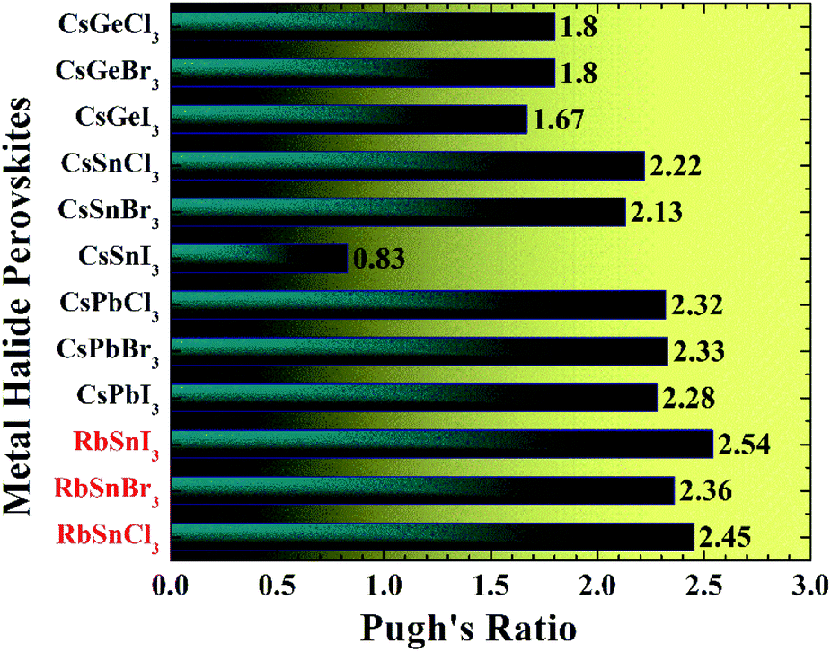 | ||
| Fig. 2 Pugh's ratio of RbSnX3 (X = Cl, Br, I) in comparison with CsBX3 (B = Ge, Sn, Pb; X = Cl, Br, I) perovskites.4 | ||
3.3. Electronic properties
The electronic characteristics of a material are one of the most significant aspects considered for optoelectronic applications. To assess the functionality of a material for a particular application, it is necessary to systematically investigate the bandgap, bandgap type (direct or indirect), the total density of states (DOS), as well as partial density of states (PDOS). Furthermore, by examining these characteristics for a set of materials, the required characteristics for optoelectronic applications can be tuned.4,15 We estimate the electronic bandgap by using the GGA-PBE approach and the results are presented in Table 3, along with the available results obtained using the GGA–PBE and other functionals.20–24 The GGA–PBE functional may underestimate the bandgap and it is expected that a hybrid functional could give a better estimate.40 However, it has been reported that a hybrid functional only cause the shift of the conduction band towards the higher energy and consequently increases the bandgap whereas the other characteristics of the band structure remain unchanged.40 The bandgap of our considered compounds for hybrid functional has been reported in the literature20–22 and the reported values can be used for other explanations. Therefore, we have not considered the hybrid functional in bandgap calculation to avoid repeating the calculations and focused on revealing new properties. Our calculated results of the bandgap of RbSnX3 (X = Cl, Br, I) are in good agreement with the available reported results for GGA-PBE as compared in Table 3.It can be noted that the bandgap value reduces monotonically due to the replacement of halogen atoms from Cl to I. In this case, I-containing compounds have a lower bandgap value, whereas Cl-containing perovskite has a higher bandgap value. Therefore, by substituting halogen atoms, the bandgap of the considered semiconductors may be controlled in practical applications, which is a significant attribute of the materials to be used in optoelectronic devices. The computed electronic band structure, DOS, and PDOS for the considered Pb-free halide perovskites are presented in Fig. 3 and 4. Furthermore, the electronic band structure indicates that the halide perovskites under consideration are direct bandgap semiconductors since the conduction band minimum and the valence band maximum occurs at the same k-vector of the Brillouin zone; these findings suggest that these compounds might have excellent optoelectronic applications.4,15 Moreover, there seem to be no active states in the DOS at the Fermi level, implying that these materials are semiconductors, which validates the estimated electronic band structures as presented in Fig. 3a–c. The total density of states below the Fermi level or top of the valence band is determined by the p orbital of the halogen atoms, whereas the p orbital of Rb and Sn atoms dominate the lower section of the conduction band as shown in Fig. 4.
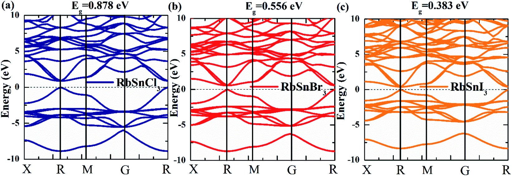 | ||
| Fig. 3 Estimated (a–c) electronic band structure of Pb free RbSnX3 (X = Cl, Br, I) metal halide perovskites. | ||
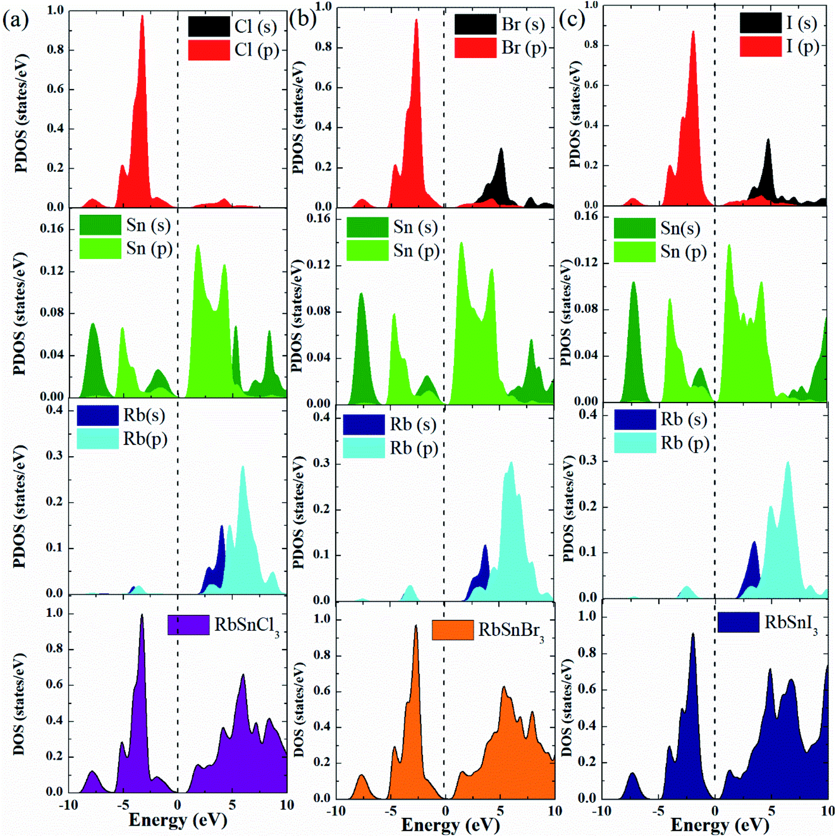 | ||
| Fig. 4 Estimated (a–c) DOS and PDOS of Pb free RbSnX3 (X = Cl, Br, I) metal halide perovskites. | ||
3.4. Optical characteristics
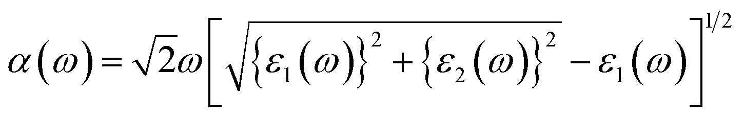
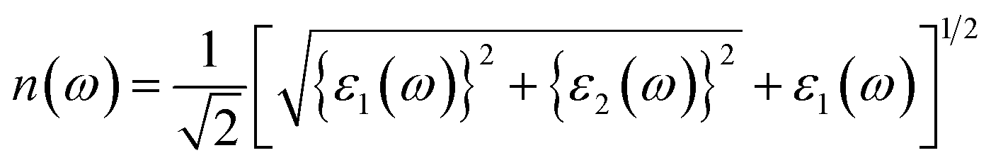
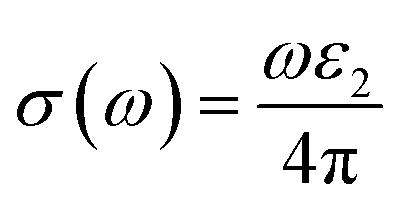
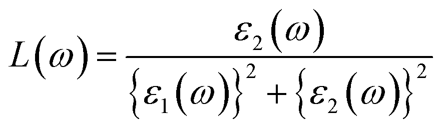
In this section, the detailed optical functions of RbSnX3 (X = Cl, Br, I), including the real and imaginary parts of dielectric functions, reflectivity, light absorption spectra, refractive index, optical conductivity, and loss function have been investigated up to 40 eV photon energy to reveal the response of RbSnX3 (X = Cl, Br, I) to solar and highly energetic radiation. It is noteworthy that the optical constants are calculated by using some well-known equations as described in the literature40,42 and implemented in the considered CASTEP code. Generally, the linear response of a test sample to electromagnetic (EM) waves is explained by the dielectric function ε(ω), which relates to the interaction of photons with electrons. Importantly, it is recognized that the imaginary portion of the dielectric function, ε2(ω), might be determined using the momentum matrix elements between the occupied and unoccupied wave functions. On the other side, the Kramer–Kronig relations are used to obtain the real portion of the dielectric function ε1(ω). Thankfully, the complex dielectric function can be used to obtain the other optical constants such as reflectivity R(ω), absorption α(ω), refractive index n(ω), optical conductivity σ(ω), loss function L(ω), and the corresponding equations are listed below .42
It is well known that the dielectric function describes a material's response to incoming EM waves and is thus essential for the successful implementation of material in optoelectronic devices. The real and imaginary parts of the dielectric constant as a function of the energy of the incident photon are displayed in Fig. 5a. A substantial shift in dielectric function is noticed as a result of the substitution of the halogen atoms. Subsequently, the I-containing compounds display the maximum peak in the infrared and visible area of the EM spectra which render it suitable for optoelectronic devices. In addition, replacing I with Br and Cl cause a move of the peaks to the high-energy range of the spectra. We emphasize that a semiconductor for photovoltaic cells must exhibit a remarkable dielectric constant, because a low dielectric constant increases the amount of electron–hole recombination, lowering the overall performance of the device.43 The y-intercept of the real part of the dielectric function (Fig. 5a) is regarded as the static dielectric function, or simply the dielectric constant. It can be noted that replacing I with Br or Cl leads to a reduction in the dielectric constant and therefore the dielectric constant of I-containing perovskite is higher compared to Br and Cl-containing perovskites.
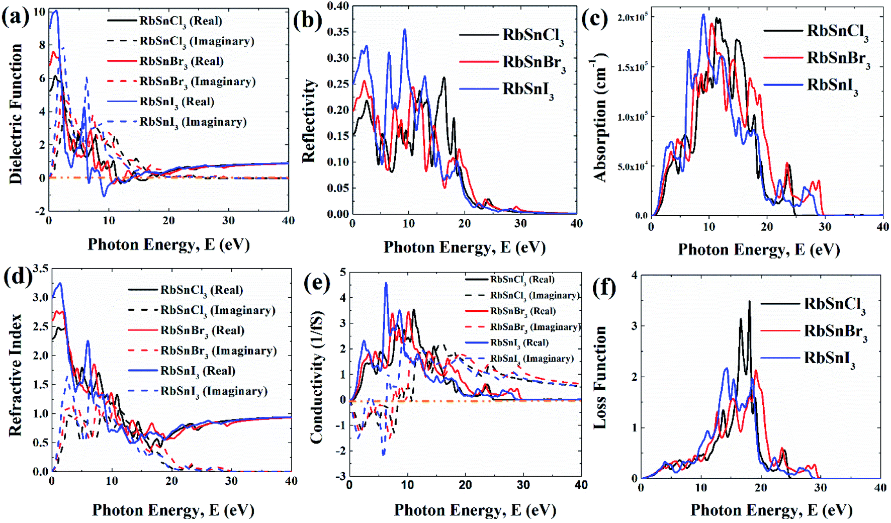 | ||
| Fig. 5 Different optical functions of RbSnX3 (X = Cl, Br, I) perovskites; (a) dielectric function, (b) reflectivity, (c) absorption, (d) refractive index, (e) conductivity, and (f) loss function. | ||
Reflectivity is another important optical parameter for photovoltaic modules and other perovskite systems.44 In the infrared-visible-ultraviolet region of the EM spectrum, all of the examined halide perovskites have a low reflectivity (<35%) as shown in Fig. 5b. Generally, a material's optical absorption quantifies the amount of light of particular energy (wavelength) that may pass through it before being absorbed.44 Also, it offers valuable insights into the solar energy conversion efficiency, which is significant to be used in solar cells.4,8 In general, all compounds have four light absorption peaks as shown in Fig. 5c. The substitution of I with Br and Cl, cause the peaks to shift to the higher energy band. Moreover, the majority of the compounds have excellent absorption in the energy range of 8–16 eV. Importantly, I-containing halide perovskite demonstrates marginally higher absorption in the low energy area (<4 eV), followed by Br and Cl-containing perovskites which suggests that I-containing halide perovskite might have outstanding optoelectronic performance compared to other halogen-containing groups.
The optical conductivity, however, is an excellent reflection of photoconductivity.45 Fig. 5e shows the real and imaginary portions of the optical conductivity. I-based perovskite compounds, as can be seen, have a strong optical conductivity (real part) in the low energy range, followed by Br and Cl-containing perovskites. Afterward, we also estimate the refractive index and loss function for the materials which has been presented in Fig. 5d and f, respectively. The prominent refractive index and lower loss function of I-containing perovskite render it more suitable for solar cell applications compared to the Cl and Br-containing groups.
Finally, the maximum absorption coefficient, as well as the optical conductivity of RbSnX3 (X = Cl, Br, I), have been compared to prior studies4 of Cs-containing perovskites as presented in Fig. 6. Note that the strongest peak in the ultraviolet zone (>3.1 eV) of the absorption and conductivity plots has been designated as the highest absorption, and conductivity, respectively. Impressively, it has been found that our studied perovskites might have excellent optoelectronic aspects as evidenced by the highest absorption coefficient and optical conductivity. Moreover, RbSnI3 exhibits remarkable light absorption capabilities as well as optical conductivity in the ultraviolet zone, which makes it suitable for ultraviolet photodetection applications.
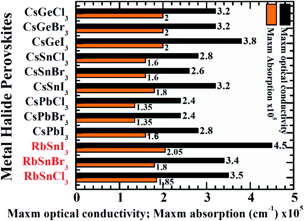 | ||
| Fig. 6 The utmost optical conductivity and maximum absorption of RbSnX3 (X = Cl, Br, I) in comparison with CsBX3 (B = Ge, Sn, Pb and X = Cl, Br, I) perovskites. | ||
4. Conclusions
In summary, the comprehensive structural, mechanical, and optoelectronic characteristics of the Pb-free metal halide perovskites RbSnX3 (X = Cl, Br, I) have been predicted by using first-principles atomistic calculations, and the outcomes have been compared to CsBX3 (B = Ge, Sn, Pb; X = Cl, Br, I) counterparts. The obtained results demonstrate that the structural parameters of RbSnX3 (X = Cl, Br, I) can be tuned systematically by substituting halogen atoms which imply that the corresponding electronic, and optical functions can also be adjusted by choosing the appropriate halogen atom. Importantly, these perovskites are expected to be mechanically stable and also have a low shear modulus (G), bulk modulus (B) with a high B/G ratio, rendering them easier to form into thin films. Besides, the electronic band structure and DOS data confirm that these compounds exhibit semiconducting behavior and feature a direct bandgap. Another merit of these Pb-free materials is the excellent light absorption and optical conductivity, indicating that they could be used in solar panels, ultraviolet photodetectors, and other optoelectronic applications. Finally, our calculated results have been compared with prior studies of CsBX3 (B = Ge, Sn, Pb; X = Cl, Br, I) compounds which reveal that RbSnI3 exhibits outstanding ductility, absorption, and optical conductivity in this family of perovskites. Remarkable light absorption capabilities, as well as excellent optical conductivity in the ultraviolet range, implying that the RbSnI3 perovskite is an excellent candidate for ultraviolet photodetection applications.Data availability
The raw/processed data required to reproduce these findings cannot be shared at this time due to technical or time limitations.Conflicts of interest
There are no potential conflicts of interest to be disclosed.References
- M. Sessolo and H. J. Bolink, Perovskite solar cells join the major league, Science, 2015, 350(6263), 917 CrossRef CAS PubMed.
- J. Chen, S. Zhou, S. Jin, H. Li and T. Zhai, Crystal organometal halide perovskites with promising optoelectronic applications, J. Mater. Chem. C, 2016, 4(1), 11–27 RSC.
- W. Zhang, G. E. Eperon and H. J. Snaith, Metal halide perovskites for energy applications, Nat. Energy, 2016, 1(6), 16048 CrossRef CAS.
- M. Roknuzzaman, K. Ostrikov, H. Wang, A. Du and T. Tesfamichael, Towards lead-free perovskite photovoltaics and optoelectronics by ab-initio simulations, Sci. Rep., 2017, 7(1), 14025 CrossRef PubMed.
- R. X. Yang, J. M. Skelton, E. Ld Silva, J. M. Frost and A. Walsh, Assessment of dynamic structural instabilities across 24 cubic inorganic halide perovskites, J. Chem. Phys., 2020, 152(2), 024703 CrossRef CAS PubMed.
- X. Li, Y. Dan, R. Dong, Z. Cao, C. Niu and Y. Song, et al., Computational Screening of New Perovskite Materials Using Transfer Learning and Deep Learning, Appl. Sci., 2019, 9(24), 5510 CrossRef CAS.
- M. Kar and T. Körzdörfer, Computational high throughput screening of inorganic cation based halide perovskites for perovskite only tandem solar cells, Mater. Res. Express, 2020, 7(5), 055502 CrossRef CAS.
- M. Roknuzzaman, K. Ostrikov, K. Chandula Wasalathilake, C. Yan, H. Wang and T. Tesfamichael, Insight into lead-free organic-inorganic hybrid perovskites for photovoltaics and optoelectronics: A first-principles study, Org. Electron., 2018, 59, 99–106 CrossRef CAS.
- A. Kojima, K. Teshima, Y. Shirai and T. Miyasaka, Organometal Halide Perovskites as Visible-Light Sensitizers for Photovoltaic Cells, J. Am. Chem. Soc., 2009, 131(17), 6050–6051 CrossRef CAS PubMed.
- N.-G. Park, Research Direction toward Scalable, Stable, and High Efficiency Perovskite Solar Cells, Adv. Energy Mater., 2020, 10(13), 1903106 CrossRef CAS.
- F. Deschler, M. Price, S. Pathak, L. E. Klintberg, D.-D. Jarausch and R. Higler, et al., High Photoluminescence Efficiency and Optically Pumped Lasing in Solution-Processed Mixed Halide Perovskite Semiconductors, J. Phys. Chem. Lett., 2014, 5(8), 1421–1426 CrossRef CAS PubMed.
- S. D. Stranks and H. J. Snaith, Metal-halide perovskites for photovoltaic and light-emitting devices, Nat. Nanotechnol., 2015, 10(5), 391–402 CrossRef CAS PubMed.
- J. H. Noh, S. H. Im, J. H. Heo, T. N. Mandal and S. I. Seok, Chemical Management for Colorful, Efficient, and Stable Inorganic–Organic Hybrid Nanostructured Solar Cells, Nano Lett., 2013, 13(4), 1764–1769 CrossRef CAS PubMed.
- M. Roknuzzaman, J. A. Alarco, H. Wang, A. Du, T. Tesfamichael and K. Ostrikov, Ab initio atomistic insights into lead-free formamidinium based hybrid perovskites for photovoltaics and optoelectronics, Comput. Mater. Sci., 2019, 169, 109118 CrossRef CAS.
- M. Roknuzzaman, C. Zhang, K. Ostrikov, A. Du, H. Wang and L. Wang, et al., Electronic and optical properties of lead-free hybrid double perovskites for photovoltaic and optoelectronic applications, Sci. Rep., 2019, 9(1), 718 CrossRef PubMed.
- P. Zhang, J. Yang and S.-H. Wei, Manipulation of cation combinations and configurations of halide double perovskites for solar cell absorbers, J. Mater. Chem. A, 2018, 6(4), 1809–1815 RSC.
- J. Jiang, C. K. Onwudinanti, R. A. Hatton, P. A. Bobbert and S. Tao, Stabilizing Lead-Free All-Inorganic Tin Halide Perovskites by Ion Exchange, J. Phys. Chem. C, 2018, 122(31), 17660–17667 CrossRef CAS PubMed.
- G. Thiele and B. Serr, Crystal structure of rubidium triiodostannate (II), RbSnI3, Z. Kristallogr. Cryst. Mater., 1995, 210(1), 64 CrossRef CAS.
- Q. Tao, P. Xu, M. Li and W. Lu, Machine learning for perovskite materials design and discovery, npj Comput. Mater., 2021, 7(1), 23 CrossRef.
- S. Körbel, M. A. L. Marques and S. Botti, Stability and electronic properties of new inorganic perovskites from high-throughput ab initio calculations, J. Mater. Chem. C, 2016, 4(15), 3157–3167 RSC.
- X. Mao, L. Sun, T. Wu, T. Chu, W. Deng and K. Han, First-Principles Screening of All-Inorganic Lead-Free ABX3 Perovskites, J. Phys. Chem. C, 2018, 122(14), 7670–7675 CrossRef CAS.
- Z. Yi, N. H. Ladi, X. Shai, H. Li, Y. Shen and M. Wang, Will organic–inorganic hybrid halide lead perovskites be eliminated from optoelectronic applications?, Nanoscale Adv., 2019, 1(4), 1276–1289 RSC.
- D. Jain, S. Chaube, P. Khullar, S. Goverapet Srinivasan and B. Rai, Bulk and surface DFT investigations of inorganic halide perovskites screened using machine learning and materials property databases, Phys. Chem. Chem. Phys., 2019, 21(35), 19423–19436 RSC.
- K. Khan, J. Sahariya and A. Soni, Structural, electronic and optical modeling of perovskite solar materials ASnX3 (A = Rb, K; X = Cl, Br): First principle investigations, Mater. Chem. Phys., 2021, 262, 124284 CrossRef CAS.
- P. Hohenberg and W. Kohn, Inhomogeneous Electron Gas, Phys. Rev., 1964, 136(3B), B864–B871 CrossRef.
- W. Kohn and L. J. Sham, Self-Consistent Equations Including Exchange and Correlation Effects, Phys. Rev., 1965, 140(4A), A1133–A1138 CrossRef.
- M. D. Segall, P. J. D. Lindan, M. J. Probert, C. J. Pickard, P. J. Hasnip and S. J. Clark, et al., First-principles simulation: ideas, illustrations and the CASTEP code, J. Phys.: Condens. Matter, 2002, 14(11), 2717–2744 CrossRef CAS.
- F. Chiter, V. B. Nguyen, N. Tarrat, M. Benoit, H. Tang and C. Lacaze-Dufaure, Effect of van der Waals corrections on DFT-computed metallic surface properties, Mater. Res. Express, 2016, 3(4), 046501 CrossRef.
- B. Liu, L. Cheng, L. Curtiss and J. Greeley, Effects of van der Waals density functional corrections on trends in furfural adsorption and hydrogenation on close-packed transition metal surfaces, Surf. Sci., 2014, 622, 51–59 CrossRef CAS.
- B. Vlaisavljevich, J. Huck, Z. Hulvey, K. Lee, J. A. Mason and J. B. Neaton, et al., Performance of van der Waals Corrected Functionals for Guest Adsorption in the M2(dobdc) Metal–Organic Frameworks, J. Phys. Chem. A, 2017, 121(21), 4139–4151 CrossRef CAS PubMed.
- J. P. Perdew, K. Burke and M. Ernzerhof, Generalized Gradient Approximation Made Simple, Phys. Rev. Lett., 1996, 77(18), 3865–3868 CrossRef CAS PubMed.
- H. J. Monkhorst and J. D. Pack, Special points for Brillouin-zone integrations, Phys. Rev. B, 1976, 13(12), 5188–5192 CrossRef.
- D. Vanderbilt, Soft self-consistent pseudopotentials in a generalized eigenvalue formalism, Phys. Rev. B, 1990, 41(11), 7892–7895 CrossRef PubMed.
- T. H. Fischer and J. Almlof, General methods for geometry and wave function optimization, J. Phys. Chem., 1992, 96(24), 9768–9774 CrossRef CAS.
- J. Kratochvil, Finite-Strain Theory of Crystalline Elastic-Inelastic Materials, J. Appl. Phys., 1971, 42(3), 1104–1108 CrossRef CAS.
- J. F. Nye. Physical properties of crystals: their representation by tensors and matrices: Oxford university press; 1985 Search PubMed.
- M. Jamal, S. Jalali Asadabadi, I. Ahmad and H. A. Rahnamaye Aliabad, Elastic constants of cubic crystals, Comput. Mater. Sci., 2014, 95, 592–599 CrossRef CAS.
- On the stability of crystal lattices. I. Mathematical Proceedings of the Cambridge Philosophical Society, ed. M. Born, Cambridge University Press, 1940 Search PubMed.
- D. Halliday, R. Resnick and J. Walker. Fundamentals of physics, John Wiley & Sons, 2013 Search PubMed.
- M. N. H. Liton, M. Roknuzzaman, M. A. Helal, M. Kamruzzaman, A. K. M. F. U. Islam and K. Ostrikov, et al., Electronic, mechanical, optical and photocatalytic properties of perovskite RbSr2Nb3O10 compound, J. Alloys Compd., 2021, 867, 159077 CrossRef CAS.
- M. Z. Rahaman and A. K. M. Akther Hossain, Effect of metal doping on the visible light absorption, electronic structure and mechanical properties of non-toxic metal halide CsGeCl3, RSC Adv., 2018, 8(58), 33010–33018 RSC.
- M. Hadi, R. Vovk and A. Chroneos, Physical properties of the recently discovered Zr2(Al1−xBix)C MAX phases, J. Mater. Sci.: Mater. Electron., 2016, 27, 11925–11933 CrossRef CAS.
- X. Liu, B. Xie, C. Duan, Z. Wang, B. Fan and K. Zhang, et al., A high dielectric constant non-fullerene acceptor for efficient bulk-heterojunction organic solar cells, J. Mater. Chem. A, 2018, 6(2), 395–403 RSC.
- M. Z. Rahaman and M. A. Islam, A Theoretical Investigation on the Physical Properties of SrPd2Sb2 Superconductor, J. Supercond. Novel Magn., 2021, 34(4), 1133–1139 CrossRef CAS.
- G. Yu, C. H. Lee, A. J. Heeger and S. W. Cheong, Photoconductivity and optical conductivity in lightly doped Nd2CuO4−δ, Phys. C, 1992, 203(3), 419–425 CrossRef CAS.
| This journal is © The Royal Society of Chemistry 2022 |