
 Open Access Article
 This Open Access Article is licensed under a Creative Commons Attribution-Non Commercial 3.0 Unported Licence
Role of processing parameters in CVD grown crystalline monolayer MoSe2†
Girija Shankar Papanaiab,
Krishna Rani Sahooc,
Betsy Reshma Gbd,
Sarika Guptae and
Bipin Kumar Gupta *ab
*ab
aPhotonic Materials Metrology Sub Division, Advanced Materials and Device Metrology Division, CSIR-National Physical Laboratory, Dr K. S. Krishnan Marg, New Delhi 110012, India. E-mail: bipinbhu@yahoo.com
bAcademy of Scientific and Innovative Research (AcSIR), Ghaziabad 201002, India
cTata Institute of Fundamental Research – Hyderabad, Sy. No. 36/P Serilingampally, Mandal, Gopanpally Village, Hyderabad 500046, India
dCSIR-Institute of Genomics and Integrative Biology, Mathura Road, New Delhi 110025, India
eMolecular Sciences Lab, National Institute of Immunology, Aruna Asaf Ali Marg, New Delhi 110067, India
First published on 4th May 2022
Abstract
The quality of as-synthesized monolayers plays a significant role in atomically thin semiconducting transition metal dichalcogenides (TMDCs) to determine the electronic and optical properties. For designing optoelectronic devices, exploring the effect of processing parameters on optical properties is a prerequisite. In this view, we present the influence of processing parameters on the lattice and quasiparticle dynamics of monolayer MoSe2. The lab-built chemical vapour deposition (CVD) setup is used to synthesize monolayer MoSe2 flakes with varying shapes, including sharp triangle (ST), truncated triangle (TT), hexagon, and rough edge circle (REC). In particular, the features of as-synthesized monolayer MoSe2 flakes are examined using Raman and photoluminescence (PL) spectroscopy. Raman spectra reveal that the frequency difference between the A1g and E12g peaks is >45 cm−1 in all the monolayer samples. PL spectroscopy also shows that the synthesized MoSe2 flakes are monolayer in nature with a direct band gap in the range of 1.50–1.58 eV. Furthermore, the variation in the direct band gap is analyzed using the spectral weight of quasiparticles in PL emission, where the intensity ratio {I(A0)/I(A−)} and trion binding energy are found to be ∼1.1–5.0 and ∼23.1–47.5 meV in different monolayer MoSe2 samples. Hence, these observations manifest that the processing parameters make a substantial contribution in tuning the vibrational and excitonic properties.
Introduction
Ultrathin two-dimensional transition metal dichalcogenides (2D-TMDCs) have attracted considerable attention over the past few years owing to their fascinating physical and chemical properties.1 The broader electron orbitals of selenide (Se2−) in comparison to sulfide (S2−) open up new avenues for numerous applications in the field of optoelectronics,2,3 logic circuits,4 and tunnel FET technology.5 Bulk MoSe2 has an indirect band gap of ∼1.1 eV and crossovers into a direct band gap of ∼1.55 eV in its monolayer form.6There are various methods to synthesize monolayer and few-layer MoSe2, including mechanical exfoliation, liquid-phase exfoliation, ion insertion, molecular beam epitaxy, hydrothermal methods, and chemical vapor deposition.7,8 Among these, chemical vapor deposition is one of the preferred methods which provides high quality, large area, uniform thickness, and desired morphology of MoSe2 flakes.9–11 However the optimization of monolayer MoSe2 becomes challenging due to poor chemical reactivity of selenium (Se) in comparison to sulfur (S). Generally, solid precursors are converted into the vapor phase during CVD growth of 2D-TMDCs, and deposited over the substrate in the solid form via molecular transport and surface diffusion processes. Recently, Kim et al. synthesized monolayer MoSe2 using a promoter assisted liquid phase CVD process in which ammonium orthomolybdate [(NH4)2MoO4] was used as a transition metal-containing precursor and potassium iodide (KI) as a promoter.12 In another study, metal chlorides, i.e., CaCl2 and SrCl2, were used as promoters to grow monolayer MoSe2.13 In addition to this, mm-size monolayer MoSe2 has been synthesized on a soda-lime glass substrate using a beam bridge transition metal precursor supply by another research group.14 Nevertheless, there are some drawbacks to using promoters for large-area synthesis, which include doping, and the formation of a metal oxide layer underneath the monolayer TMDCs.15,16
To resolve such complications, promoter-free growth has been taken into consideration in the present work. Next, in photoluminescence study of CVD-grown monolayer MoSe2, the peak position of A exciton varies from ∼1.48–1.57 eV in earlier reports.9,10,17,18 The variation in PL peak position directly affects nature of quasiparticles. In monolayer TMDCs, the quasiparticle dynamics play a significant role due to reduced dielectric screening, strong quantum confinement, and the larger effective masses of charge carriers. In a semiconductor, the fundamental optical excitation is electron–hole (e–h) pair which is bounded via Coulomb attraction called an exciton. The binding energy of exciton and trion is larger in monolayer TMDCs as compared to quasi 2D semiconductors, namely GaAs quantum well, which makes these carriers stable at ambient temperature. There are several reports on the quasiparticles dynamics and exciton–trion interaction in monolayer MoSe2.19–22 But influence of experimental parameters on the behavior of quasiparticles is still missing. To explain this, quasiparticles behavior has been examined at different growth conditions using PL emission spectroscopy.
In this work, we report the synthesis of high-quality monolayer MoSe2 flakes using a lab-built CVD setup at atmospheric pressure. The lattice dynamics and charge carrier features have been studied in detail under the influence of processing parameters in as-synthesized samples and as-obtained shapes. To the best of our knowledge, influence of experimental parameters on Raman scattering and PL in CVD-grown monolayer MoSe2 flakes is not reported yet.
Experimental section
Synthesis of MoSe2 flakes
The monolayer MoSe2 flakes have been synthesized using lab-built CVD setup in a single zone furnace. This lab-built CVD setup has also been used to synthesize the monolayer MoS2 flakes in our previous work.23 Prior to synthesis, SiO2/Si (300 nm) substrates are sonicated in acetone and isopropyl alcohol (IPA) for 10 min each to remove the surface adsorbates. Further, the substrates have been rinsed with deionized water followed by HF dip (2%) and blow-dried using N2 gas. For the reaction, solid precursors molybdenum(VI) oxide (MoO3) powder (>99%, Fisher Scientific) and selenium (Se) pellets (99.999%, CERAC) have been loaded along with SiO2/Si substrate inside the quartz tube (ID 60 mm × OD 65 mm × L 1200 mm). The MoO3 powder (15–30 mg) has been placed in alumina boat (length ∼ 9 cm) at the center of split tube furnace. Se pellets (153–305 mg) have been kept in second alumina boat at a separation of ∼20 cm from MoO3 powder on upstream side of furnace. The Si/SiO2 substrates have been kept upside down above MoO3 powder's loaded alumina boat towards the downstream side. The reaction chamber has been pumped down up to a base pressure of ∼2.8 × 10⁻² mbar and purged with high purity Ar gas for half an hour. After purging, H2 (10–25 sccm) and Ar (60–200 sccm) gases have been introduced in the reaction chamber at atmospheric pressure and constantly maintained till the cooling process. The temperature of furnace has been heated gradually up to 770–810 °C within 70 min and hold for 15–32 min. After the growth, furnace has been opened at 600 °C and allowed to cool naturally in the presence of Ar and H2 gas up to 100 °C. After cooling, samples have been taken out and used for further characterizations.Transfer of MoSe2 flakes on TEM grid
The MoSe2 flakes are transferred on holey carbon Cu TEM grid using HF. The shiny/dark side of TEM grid is put over Si/SiO2 substrate in the region where flakes need to be transferred. The 5% HF solution is drop casted on the region of TEM grid using a micropipette and wait for 30 s. After this step, the TEM grid with MoSe2 flakes has soaked in DI water for several times and dried at ambient condition.Characterization
The XRD system Rigaku (MiniFlex II) is used to record the diffraction pattern of MoO3 and Se precursors with Cu Kα1 (λ = 1.5418 Å) as a radiation source. Optical microscopy has been used to visualize the synthesized MoSe2 monolayer over Si substrate having a SiO2 thickness of 300 nm (GMS-India). The LEXT 3D measuring laser microscope OLS5100 has been used in the bright field mode with objective lenses MPLAPON50XLEXT, MPLAPON100XLEXT having NA, and the working distance of 0.95 and 0.35 mm, respectively. Additionally, Leica DM 2700M equipped with Raman microscope has also been used to capture optical images in bright field mode with 50× and 100× magnification. Further, the surface morphologies of synthesized MoSe2 flakes have been probed using scanning electron microscopy (FESEM Model: JEOL, JSM-7200F) under an acceleration voltage of 5–25 kV. For measuring the thickness of MoSe2 flakes, atomic force microscope (AFM Model: Keysight 5500) has been used in contact mode. The TEM images and diffraction patterns have been captured with FEI Tecnai TF20 (accelerating voltage: 200 kV) equipped with a field-emission gun (FEG) source and a 4k × 4k Eagle CCD Camera. The chemical states are examined at room temperature using ESCA+ (Omicron Nanotechnology, Oxford Instrument Germany) equipped with monochromatic Al Kα source (hν = 1486.7 eV). The binding energy of C 1s core (284.6 eV) is taken as a reference, and a charge neutralizer of 2 keV is applied to overcome the charging problem. UV-visible absorption spectrum of the MoSe2 flakes has been recorded using a UV-vis spectrometer (AvaLight-DH-S-BAL) to study the optical transitions. Raman and PL measurements have been employed using the Renishaw inVia™ confocal Raman microscope with 50× magnification at ambient condition. The Raman spectra have been recorded using an excitation laser wavelength of 532 nm, having the power of 2.5 mW under exposure time of 10 s with 2400 l mm−1 grating, respectively. The PL spectra have been captured using an excitation wavelength of 633 nm having laser power of 5 mW under exposure time of 10 s with 1800 l mm−1 grating, respectively.Results and discussion
The monolayer MoSe2 flakes have been synthesized using the lab-built CVD setup in a single zone furnace. The schematic diagram of synthesis of MoSe2 flakes using solid MoO3 and Se precursors by the CVD method has been shown in Fig. S1 in the ESI,† where the notations are in their usual meaning. Prior to synthesis, MoO3 and Se precursors are also examined using XRD, as displayed in Fig. S2 (in the ESI).† Past study interpreted that the synthesis of monolayer MoSe2 takes place only when H2 gas is introduced in the reaction chamber.24 Here, H2 gas plays a key role in creating a reducing environment for MoO3 in addition to Se and facilitates the growth of MoSe2 monolayer. The formation of monolayer MoSe2 occurs on the substrate via reaction of MoO3 and Se in the presence of Ar and H2 gas. With a similar analogy of MoS2 formation, the plausible stepwise reaction can be expressed by the following equations:25
 | (1) |
 | (2) |
| Sample name | Growth temperature (°C) | MoO3 powder (mg) | Se pellets (mg) | H2 flow (sccm) | Ar flow (sccm) | Deposition time (min) |
|---|---|---|---|---|---|---|
| MS-1 | 770 | 30 | 305 | 20 | 60 | 30 |
| MS-2 | 770 | 20 | 252 | 15 | 60 | 20 |
| MS-3 | 780 | 20 | 185 | 20 | 200 | 32 |
| MS-4 | 780 | 15 | 155 | 20 | 60 | 20 |
| MS-5 | 780 | 15 | 172 | 20 | 60 | 20 |
| MS-6 | 790 | 15 | 153 | 15 | 60 | 20 |
| MS-7 | 800 | 25 | 248 | 25 | 100 | 30 |
| MS-8 | 810 | 30 | 302 | 10 | 60 | 15 |
 | ||
| Fig. 1 The optical images of eight different CVD-grown monolayer MoSe2 samples are named MS-1 to MS-8, deposited on Si substrate having SiO2 thickness of 300 nm. (a and b) Sample MS-1. (c and d) Sample MS-2. (e and f) Sample MS-3. (g and h) Sample MS-4. (i and j) Sample MS-5. (k and l) Sample MS-6. (m and n) Sample MS-7. (o and p) Sample MS-8. | ||
 | ||
| Fig. 2 SEM images of CVD grown monolayer MoSe2 samples over Si/SiO2 substrate: (a and b) sample MS-3. (c and d) Sample MS-4. (e–i) Sample MS-5. (j–l) Sample MS-6. | ||
Next, the surface morphology of sample MS-4 shows identical REC shapes with high uniformity. It is generally known, the compactness of any shape is defined by the area to perimeter ratio, and the REC has the large compactness.
The formation of REC shape resulted from the high growth rate of both Mo and Se edges, suggesting that both edges have insufficient time to diffuse on the preferable location of the lattice. Under the Se rich atmosphere, Mo atoms have more probability of attaching with Se atom instead of another incoming Mo atom at the flake edge; enhance the lateral growth. One can notice from the surface morphologies that the nucleation takes place on substrate in a random manner. However, color contrast in each sample indicates that the monolayer flakes are formed with high uniformity (see Fig. 1). After the nucleation process, monolayer growth takes place via attachment and diffusion of adsorbed atoms on substrate. Quantitatively, distribution of adsorbed atoms and the growth rate can be represented by the following diffusion equation:26
 | (3) |
 and adsorbed atom supply rate (F), the growth in lateral direction can be controlled. As the flow rate of H2 and Ar gases increases, the number of adsorbed atoms enhances. Consequently, probability of nucleation becomes higher on the substrate. At the moment of high flow rate of H2 gas, the formation of MoO3−x speeds up along with the excess Se vapor in reacting region, which makes more coverage of MoSe2 flakes over the substrate. In case of low flow rate of H2 gas, the amount of Se vapors can not transport sufficiently, and probability of MoSe2 coverage over the substrate becomes lower. However, the shapes are not transformed into perfect ST, TT, REC, and hexagon at a low H2 flow rate (MS-8). On the other hand, most regions are covered by the hexagons (MS-7) at a high flow rate of H2 gas. The effect of H2 flow on MoSe2 flakes has been previously reported in detail by another research group.27 Next, variation in temperature from 770 °C to 810 °C increases the evaporation rate of precursors which directly influence growing rate of Mo and Se edge. Consequently, difference in Mo and Se edge termination creates varying shapes on the substrate. Further, in the course of a high flow rate of Ar gas, smoothening on the flake side is minimized (MS-3). Moreover, as growth time increases, MoSe2 flakes start to merge together and form the large area monolayer (MS-1 and MS-3). In addition to this, merging of flakes is also appeared in other samples owing to the high precursor's weight ratio (MoO3
![[thin space (1/6-em)]](https://www.rsc.org/images/entities/char_2009.gif) :Se). One would conclude from these observations, the shape of MoSe2 flakes can be tailored by varying processing parameters.
:Se). One would conclude from these observations, the shape of MoSe2 flakes can be tailored by varying processing parameters.
Now, we turn our attention towards the crystal structure of monolayer MoSe2 and different atomic arrangements in obtained shapes. The crystal structure of monolayer MoSe2 consists of a 2D hexagonal lattice, where Mo and Se atoms are arranged in trigonal prismatic coordination (Fig. 3a). Further, the possible atomic arrangements in different as-synthesized shapes (ST, TT, hexagon, and REC) are represented in Fig. 3b–f. Fig. 3b and c show the atomic arrangements with Mo-zz termination and Se-zz termination in ST shape. One can observe the difference in the arrangement of Mo and Se atoms in TT, hexagon, and REC (see Fig. 3d–f). Based on the slowest and fastest-growing faces (Mo-zz and Se-zz), one can determine the shape of MoSe2 flakes. The transformation from ST to REC shapes is a direct consequence of the surface energies of both Mo and Se edges. Apart from this, the variation in shape of MoSe2 flakes is ascribed to the change in Mo:Se ratio of precursors.
 | ||
| Fig. 3 (a) Top view of crystal structure of monolayer MoSe2. The pictorial diagram of Mo and Se atomic arrangements in different shapes of as-synthesized monolayer MoSe2 flakes: ST with (b) Mo-zz and (c) Se-zz termination; (d) TT, (e) hexagon, and (f) REC. | ||
In order to examine the quality and number of layers of as-synthesized MoSe2 flakes, Raman spectroscopy has been carried out. Fig. 4a shows Raman spectra of as-synthesized MoSe2 flakes over Si/SiO2 and quartz substrate. The Raman spectra are captured at the center of the MoSe2 flakes. The most pronounced single component peak (A1g) has been found at 239.75 and 239.89 cm−1 in Si/SiO2 and quartz substrate, respectively. One can observe the A1g mode intensity is higher in Si/SiO2 substrate than quartz substrate. The other major Raman modes are observed at 170.53 cm−1 (E1g), 250.28 cm−1 (second-order Raman mode) and 286.93 cm−1 (E12g) over Si/SiO2 substrate. The MoSe2 monolayer belongs to the space group D13h and in case of the monolayer, the irreducible representation of the Γ phonons is described by  . At Γ point, MoSe2 monolayer has the nine-phonon modes having six-optical and three-acoustic branches.28 The Raman active modes A1g
  relates to the out of plane vibrations of Se atoms and E12g (E′) is attributed to in plane vibrations of Mo and Se atoms. The E′′ and
  modes are not Raman active in monolayer. The peak appeared close to 250 cm−1 is second order Raman mode owing to double resonance process. The frequency difference between A1g and peak close to 250 cm−1, A1g and E12g peaks are found to be ∼10.53 cm−1 and ∼47.18 cm−1; the peak intensity close to ∼170 and ∼360 cm−1 is found to be negligible as compared to A1g peak (see Fig. 4a).These above mentioned features confirms that the synthesized MoSe2 flakes are monolayer in nature and agrees well with the previous reports.29,30 Fig. 4b and c displays Raman spectra of different samples (MS-1 to MS-8) and different as-obtained shapes, i.e., ST, TT, hexagon, and REC of monolayer MoSe2 at the center location. The frequency difference between A1g and peak close to 250 cm−1 is found to be >10 cm−1 suggesting that the as-synthesized samples and as-obtained shapes are monolayers in nature. The peak frequencies of A1g and E12g Raman modes, along with their frequency differences in different as-synthesized samples and as-obtained shapes of monolayer MoSe2 have been shown in Fig. 4d and e. The frequency difference between these two modes has been found to be >45 cm−1 which further confirms that the as-synthesized samples and as-obtained shapes are monolayers in nature.30 The peak frequency of A1g and E12g Raman modes vary from 239.52 to 240.91 cm−1 in as-synthesized samples and 284.83 to 287.38 cm−1 in as-obtained shapes, respectively. One can notice that the variation in experimental parameters does not affect the frequency of A1g mode significantly. Moreover, to more thoroughly examine the uniformity of A1g vibrational mode, Raman mapping has been employed. Fig. 4f–h illustrates Raman mapping in sample MS-3, and the intensity map shows the uniform color contrast at centre as well as edge, as depicted in Fig. 4f. The peak position map displays different color contrast at edge and middle region, as can be seen from Fig. 4g. The peak width map reveals the nearly uniform contrast except some regions nearby centre, as shown in Fig. 4h. Fig. 4i–k shows the Raman mapping in sample MS-5 and color contrast shows the small variation in few locations in peak intensity, peak position and peak width mapping. It can be noticed that Raman mapping of A1g mode shows higher uniformity in MS-3 as compared to MS-5. These observations clearly confirm that the as-synthesized samples are high in quality. Further, AFM has been employed to examine the uniformity and thickness of monolayer MoSe2 flakes over Si/SiO2 substrate, which is shown in Fig. S3 (in the ESI).† Next, TEM has been carried out to examine the crystalline structure of CVD-grown MoSe2 flakes. Fig. 5a shows the bright field plan-view TEM image of MoSe2 flake having REC shape at low magnification. The high-resolution TEM (HRTEM) image is shown in Fig. 5b, and inset shows the enhanced view of lattice fringe which is marked by rectangular region. The lattice spacing is measured from the HRTEM image and found to be ∼0.28 nm, which corresponds to {10
![[1 with combining macron]](https://www.rsc.org/images/entities/char_0031_0304.gif) 0} planes. Fig. 5c displays the selected area electron diffraction (SAED) pattern within the REC shape, having one set of diffraction spots with six-fold symmetry. These features confirm that the synthesized monolayer MoSe2 flakes are single crystalline in nature. From the SAED pattern, one can also compute the lattice spacing corresponds to {100} and {11
0} planes. Fig. 5c displays the selected area electron diffraction (SAED) pattern within the REC shape, having one set of diffraction spots with six-fold symmetry. These features confirm that the synthesized monolayer MoSe2 flakes are single crystalline in nature. From the SAED pattern, one can also compute the lattice spacing corresponds to {100} and {11![[2 with combining macron]](https://www.rsc.org/images/entities/char_0032_0304.gif) 0} planes, which are determined to be ∼0.28 nm and ∼0.16 nm and agree well with previous reports.2,10,24 Furthermore, to examine the oxidation states and atomic ratio in an as-synthesized monolayer MoSe2, X-ray photoelectron spectroscopy (XPS) has been carried out. The survey scan of as-synthesized MoSe2 flakes deposited over Si/SiO2 substrate is displayed in Fig. 6. The core-level spectra of Mo 3d and Se 3d are displayed in Fig. 7a and b. The spectra are fitted with the Gaussian–Lorentzian function, and the estimated background is Shirley type. The Mo 3d spin–orbit doublet comprises two peaks Mo 3d5/2 ∼ 228.5 eV and Mo 3d3/2 ∼ 231.8 eV, which corresponds to Mo4+ 3d states.
0} planes, which are determined to be ∼0.28 nm and ∼0.16 nm and agree well with previous reports.2,10,24 Furthermore, to examine the oxidation states and atomic ratio in an as-synthesized monolayer MoSe2, X-ray photoelectron spectroscopy (XPS) has been carried out. The survey scan of as-synthesized MoSe2 flakes deposited over Si/SiO2 substrate is displayed in Fig. 6. The core-level spectra of Mo 3d and Se 3d are displayed in Fig. 7a and b. The spectra are fitted with the Gaussian–Lorentzian function, and the estimated background is Shirley type. The Mo 3d spin–orbit doublet comprises two peaks Mo 3d5/2 ∼ 228.5 eV and Mo 3d3/2 ∼ 231.8 eV, which corresponds to Mo4+ 3d states.
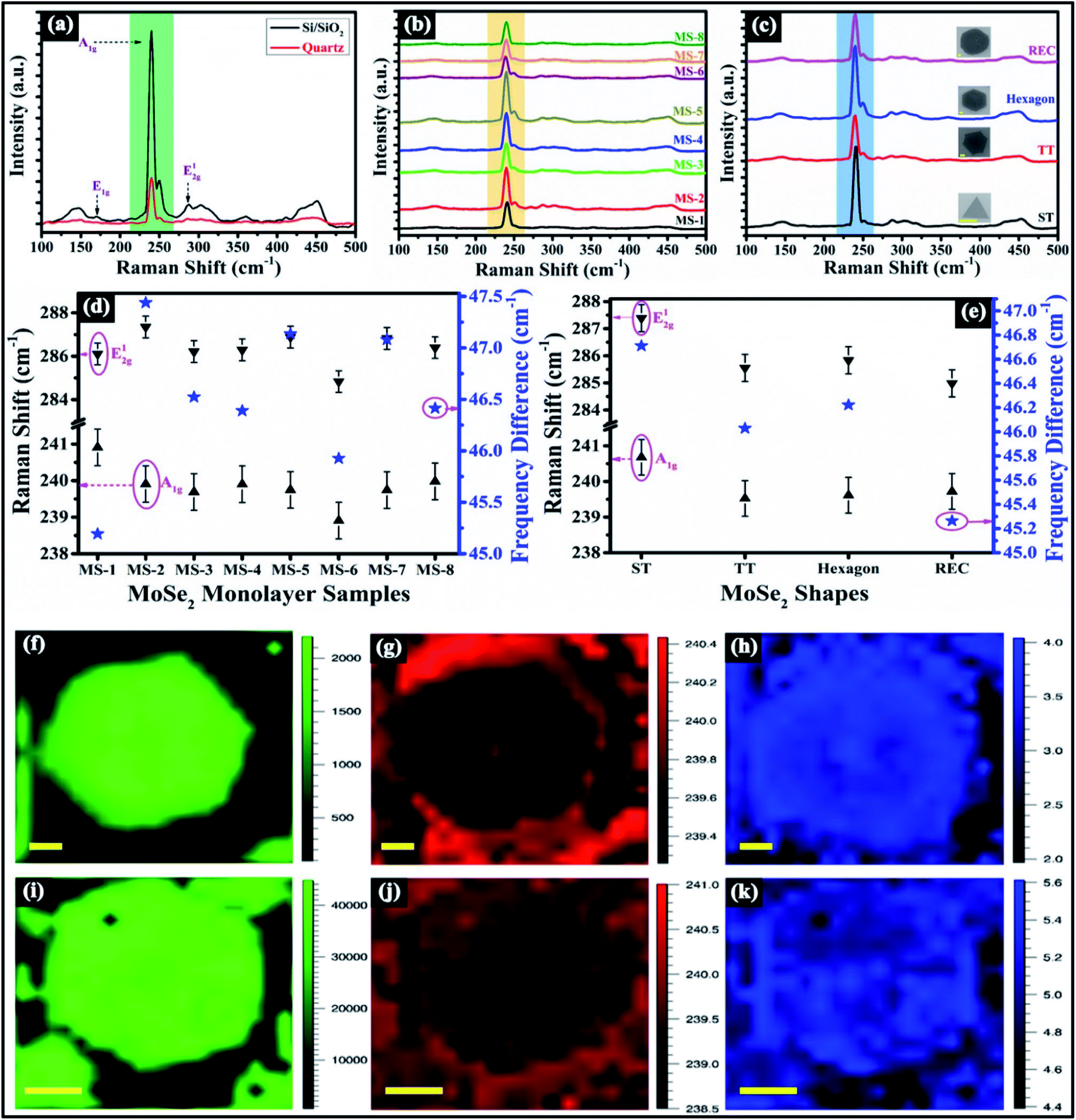 | ||
| Fig. 4 (a) Raman spectrum of monolayer MoSe2 flakes on the Si/SiO2 and quartz substrate. (b) Raman spectra of different monolayer MoSe2 samples (MS-1 to MS-8) over Si/SiO2 substrate and vertically stacked for clarity. (c) Raman spectra of as-obtained shapes such as ST, TT, hexagon, and REC of monolayer MoSe2 over Si/SiO2 substrate. The Raman spectra are stacked vertically for clarity, and the scale bar in each shape is 2 μm. Peak position variation of A1g and E12g Raman modes (left vertical axis) and their frequency difference (right vertical axis): (d) in as-synthesized samples and (e) in as-obtained shapes. Raman mapping in sample MS-3: (f) peak intensity, (g) peak position, and (h) peak width. Raman mapping in sample MS-5: (i) peak intensity, (j) peak position, and (k) peak width. The scale bar is 5 μm in each mapped image. | ||
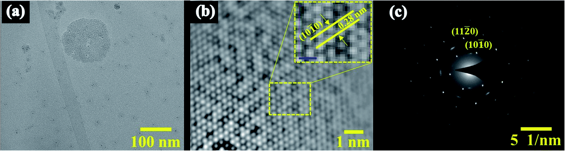 | ||
| Fig. 5 (a) The bright-field TEM image of transferred monolayer MoSe2 flake having REC shape. (b) HRTEM image of the REC shape and inset shows the enhanced view of the atomic arrangement of Mo and Se atoms with a scale bar of 0.5 nm. (c) SAED pattern confirms the hexagonal symmetry of the MoSe2 structure. | ||
 | ||
| Fig. 6 Survey scan is captured on the as-synthesized monolayer MoSe2 flakes deposited on the Si/SiO2 substrate. The identified elements are marked. | ||
 | ||
| Fig. 7 High-resolution XPS spectra of (a) Mo 3d and (b) Se 3d recorded at room temperature. | ||
Additionally, a relatively more minor amount of MoO3 is expectedly present in MoSe2 flakes, confirmed by the appearance of the binding energy peaks at 232.7 eV (3d5/2) and 235.7 eV (3d3/2) of Mo6+ charge states and agrees well with Mo6+ oxidation state from α-MoO3.31 The Se 3d spectra at the binding energy of ∼54.7 eV and 55.7 eV relate with the doublets core level 3d5/2 and 3d3/2, which belongs to the Se2− oxidation state of selenium.
One can observe that the Mo6+ 3d state and Se2− 3s state overlap with the Mo4+ 3d states.32 The above-mentioned features closely match with the earlier published literature of CVD-grown monolayer MoSe2.10,33,34 In order to estimate the atomic ratio, the integrated peak areas of Mo4+ 3d and Se2− 3d peaks have been taken into consideration, and peak areas are normalized with respect to the atomic sensitivity factor. The estimated Se/Mo ratio is found to be ∼1.8, indicating a large amount of Se vacancies are present in as-synthesized MoSe2 flakes.
Further, in order to determine the optical transitions, the absorption spectrum is collected on monolayer MoSe2 flakes over the quartz substrate, as shown in Fig. S4 (in the ESI).†
Moreover, photoluminescence is another robust technique to characterize the quality of the as-synthesized MoSe2 flakes. Fig. 8a shows the PL spectra of monolayer MoSe2 over Si/SiO2 and quartz substrate at room temperature. The prominent emission peak is found to be at ∼799.35 nm (1.55 eV) on Si/SiO2 and ∼792.58 nm (1.56 eV) on a quartz substrate. The strong emission peak is attributed to the direct transition at the K point of the Brillouin zone, and the direct band gap emission is corroborated with the previous reports of the monolayer MoSe2.24,27 A red shift has been observed in PL peak position on Si/SiO2 substrate, and PL intensity is reduced approximately seven times compared to the quartz substrate. The strong PL intensity on quartz substrate is owing to the availability of rich electron density, which induces more excitons formation. It is worth noting that a broader tail at high wavelength side and a steep edge at the lower wavelength side in PL emission. Furthermore, Fig. 8b and c illustrate the PL spectra of different as-synthesized samples and as-obtained shapes. In each sample, the PL spectrum is recorded at the center of flake. In both the figures, displayed spectra are collected at one location of monolayer MoSe2. It is interesting to note that the PL intensity of MS-7 is more pronounced as compared to other samples (see Fig. 8b). On the other side, REC shape exhibits most prominent PL feature among all the obtained shapes. The peak position of A exciton along with the normalized PL in as-synthesized samples and as-obtained shapes is displayed in Fig. S5a and b (in the ESI).† The significant shift has been observed in A exciton peak energy which is in range of ∼1.52–1.57 eV, as described in Fig. S5a (in the ESI).† It can be noticed that A exciton peak is observed in the range of ∼1.506–1.514 eV in as-obtained shapes. The as-obtained shapes which are displayed in Fig. S5b (in the ESI),† belong to sample MS-6. In addition to this, the distinct shapes have been analyzed in each sample and found that the A exciton peak lies within the range of ∼1.50–1.58 eV, 1.50–1.52 eV, 1.50–1.56 eV, and 1.51–1.57 eV for ST, TT, hexagon, and REC shapes respectively. The excitonic quasi-particles (excitons and trions) exist together at room temperature by virtue of strong Coulomb interactions in 2D materials.
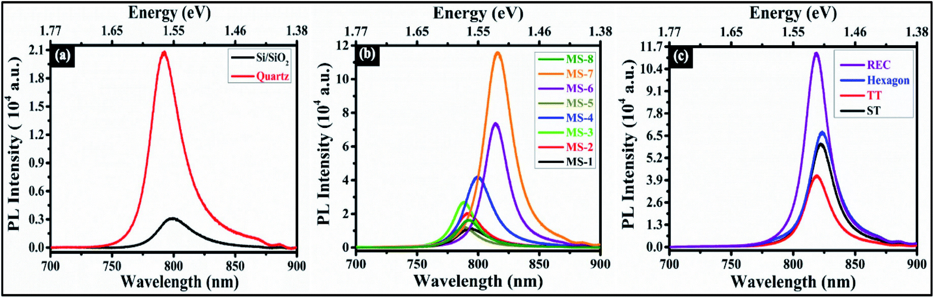 | ||
| Fig. 8 (a) PL spectrum of monolayer MoSe2 flakes over Si/SiO2 and quartz substrate. (b) PL spectra of different monolayer MoSe2 samples (MS-1 to MS-8) over Si/SiO2 substrate. (c) PL spectra of as-obtained shapes of monolayer MoSe2 flakes. | ||
The appearance of prominent excitonic features in the monolayer is attributed to the large binding energies. The large exciton binding energy occurs because of the geometrical confinement of excitonic quasiparticles in low dimensional systems, which enhance the e–h overlapping.35,36 Additionally, the interaction between charges becomes stronger as the thickness goes down; as a consequence screening effects become lower and induces the strong electron–electron correlation.37 Moreover, to examine the contribution of neutral exciton (A0) and trions (A−) in strong PL emission, the PL spectra are fitted with two Voigt functions, as shown in Fig. 9a–l. The PL emission of trion is red shifted in each case, ascribed to electron–phonon interaction. The trion emission is lower than neutral exciton emission in all the synthesized samples and different obtained shapes, depicted in Fig. 9a–l. The quasiparticle's intensity ratio {area ratio, I(A0)/I(A−)} has been found ≥2 in all the synthesized samples and obtained shapes except sample MS-8. In sample MS-8, I(A0)/I(A−) is found to be ∼1.1, suggesting that the emission of trion is almost comparable to neutral exciton emission. These observations indicate that the stronger radiative recombination takes place in samples MS-1 to MS-7 and as-obtained shapes in comparison to MS-8. The obvious difference in I(A0)/I(A−) as a consequence of the varying experimental conditions. Generally, variation in growth temperature generates a significant strain on the substrate due to which the deposited monolayer flakes are affected. In addition, the different concentration of precursors in vaporized form induce varying defect structures in as-synthesized shapes. Previously, it has been observed that the extra charges originate from doping, defects, substrate, and gate biasing.38,39 To gain more physical insight into trion binding energy, the calculation of energy difference (Δ) between A0 and A− is required. The PL peak energy position of neutral exciton and trion has been illustrated in Fig. S5c (in the ESI)† for the as-synthesized samples. The energy difference (Δ) between A0 exciton and A− trion is found to be 23.3–47.5 meV. Similarly, the excitonic peak positions in as-obtained shapes have been shown in Fig. S5d (in the ESI),† and energy difference is observed in the range of 23.1–33.5 meV, respectively. Previously, it has been seen that trion binding energy is approximately 0.1 times the exciton binding energy in monolayer TMDCs.40 In the present study, obtained trion binding energy in as-synthesized samples and as-obtained shapes are closely matched with the earlier report39 and the small shift in trion binding energy as a result of varying electron–phonon coupling strengths. These results point out that the behavior of neutral and charged exciton in PL spectra is significantly affected by experimental conditions. Moreover, Fig. 9m and n display schematic energy band diagram of neutral exciton (A0) and trion (A−). In case of A0, the electronic band gap (Eg) is sum of PL peak energy (PLA0) and neutral exciton binding energy (EA0), which is expressed as Eg = PLA0 + EA0. Now, in case of charged exciton (trion), electronic band gap is described as Eg = PLA− + EA0 + EA−, where EA− is the binding energy of A− trion. Here, excitation energy of 1.96 eV is used to capture PL spectra and which is larger than the band gap. When the bound e− is promoted in the conduction band via interaction of light, the high energy e− loses energy in form of thermal energy and settles down in the minimum energy state in the conduction band (conduction band minimum), as shown in Fig. 9m and n. As similar, the thermalization loss occurs in valence band also, holes move towards their minimum energy state, which is the top of valence band (valence band maximum).
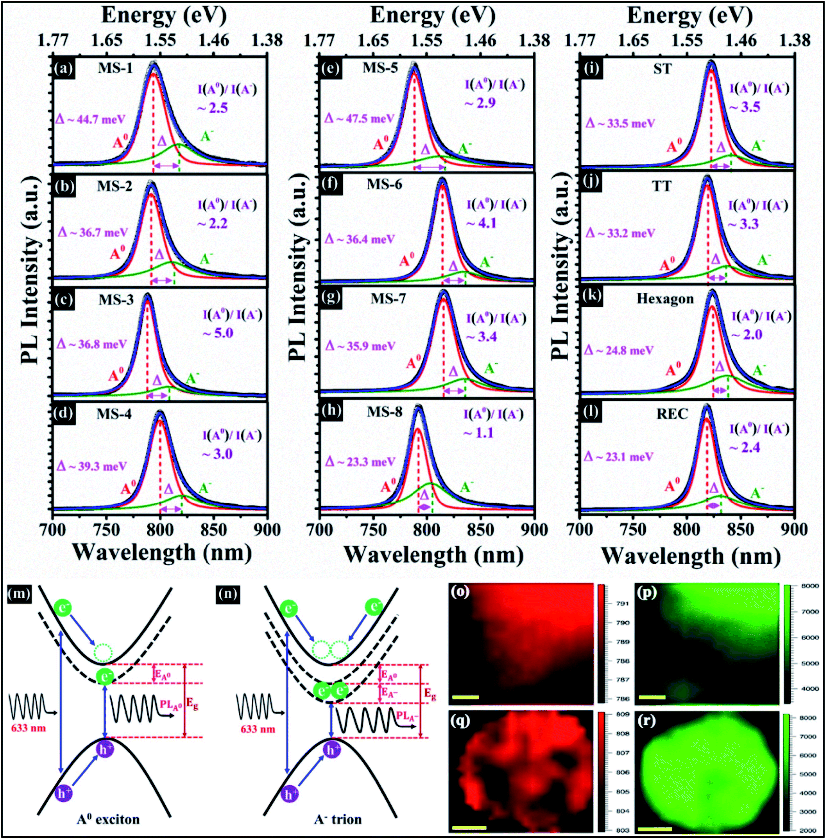 | ||
| Fig. 9 PL spectra are deconvoluted for obtaining the neutral exciton and charge exciton contribution: (a–h) as-synthesized samples (MS-1 to MS-8) and (i–l) as-obtained shapes. Experimental data, fitted data, A0 exciton PL peak, and A− trion PL peak are represented by circular dots (black), blue lines, red lines, and green lines, respectively, where Δ is the energy difference between A0 exciton and A− trion. Schematic diagram of the excitonic transitions: (m) A0 exciton formation and (n) A− trion formation. Here EA0, EA−, Eg, PLA0, and PLA−, denote the A0 exciton binding energy, A− trion binding energy, electronic band gap, PL peak energy of A0 exciton, and A− trion. In the case of A0, the electronic band gap (Eg) is the sum of PL peak energy (PLA0) and the neutral exciton binding energy (EA0), which is expressed as Eg = PLA0 + EA0. For charged exciton (trion), the electronic band gap is described as Eg = PLA− + EA0 + EA−. PL mapping in the edge of large-area monolayer MoSe2: (o) peak position and (p) peak intensity. PL mapping in the REC shape: (q) peak position and (r) peak intensity. | ||
However, in semiconductors, there are two mechanisms of exciton formation which are mainly taken into consideration: (a) high kinetic energy exciton generates the photon along with phonon emission concurrently, the e–h recapitulate during this process;41 (b) formation of bi-molecular exciton.42 But in case of monolayer TMDCs, the recapitulation of e–h only takes place when excitation energy is lower than the free particle band gap. When carrier densities becomes high, probability of the scattering (elastic or inelastic) with free carriers is enhanced. A new state comes in to the existence as inelastic scattering occurs between free charge carriers and exciton. Throughout this process, excitons gained extra charge and created the trion states. Furthermore, PL mapping has been carried out over MoSe2 flakes to probe the crystal quality. Fig. 9o–r shows the PL maps with respect to peak position and peak intensity of A exciton in edge of large area MoSe2. The color contrast of peak position map exhibits boundary of a large area, which has a slight difference as compared to centre of a large area, as shown in Fig. 9o. In the peak intensity map, PL intensity becomes lowers towards boundary of a large area and enhances at the central part, illustrated in Fig. 9p. The PL peak position and peak intensity images of A excitonic peak in REC shape have been illustrated in Fig. 9q and r. The color contrast of REC shape displays the uniform region except few darker regions where the PL peak positions are blue shifted (see Fig. 9q). The PL intensity map reveals that intensity is uniform in almost all the regions aside from some of the small patches, as can be seen from Fig. 9r. In addition, PL peak position and peak intensity maps on the distorted hexagonal shape have been shown in Fig. S6 (in the ESI).† The PL position and intensity maps imply that the as-synthesized samples are high in quality and monolayer in nature.
Hence, present work offers a platform for the optical tuning of excitonic emission in CVD-grown monolayer MoSe2 and exploring the applications in field of optoelectronics and valleytronics.
Conclusions
In summary, we have been synthesized high-quality monolayer MoSe2 flakes using a lab-built CVD setup, and a range of shapes, namely sharp triangle, truncated triangle, hexagon, rough edge circle, have been evolved in the course of growth at different optimized conditions. The obtained morphologies of monolayer MoSe2 confirmed that the processing parameters, including growth temperature, gas flow rate, substrate's location, and growth time, played a crucial role in controlling the quality of samples. An extensive study of Raman scattering in as-synthesized samples (MS-1 to MS-8) and as-obtained shapes have been presented and confirming that prepared samples are highly uniform and monolayer in nature. Further, prominent PL emission at room temperature confirms the monolayer nature of synthesized MoSe2 flakes, where peak energy of A exciton is found to be in the range of 1.50–1.58 eV. Moreover, binding energy of trion is evaluated in monolayer MoSe2 and found to be in the range of 23.1–47.5 meV. The spectral weight of exciton and trion in PL emission directly affects the process of radiative recombination. In addition, the emission of trion has been found very weak as compared to the neutral exciton emission in most synthesized samples. Thus, this study opens up new avenues to get insight into lattice and quasiparticles dynamics under the influence of processing parameters and may pave the way in controlling the optical properties.Author contributions
Girija Shankar Papanai – conceptualization, investigation, methodology, formal analysis, writing-original draft. Krishna Rani Sahoo – Raman and PL measurements, review and editing. Betsy Reshma G – AFM measurements. Sarika Gupta – AFM measurements, review and editing. Bipin Kumar Gupta – supervision, funding acquisition, conceptualization, validation, review and editing.Conflicts of interest
There are no conflicts to declare.Acknowledgements
Authors acknowledge the Director, Prof. Venugopal Achanta, CSIR-NPL, for providing the research facility for the mission mode project on “Metrology of 2D materials for quantum devices”. We are grateful to Mr Amit Boora (OLYMPUS, Gurugram, India) and Dr Sudhir Husale for their continuous support in the Optical Microscopy facility. We thank Dr Preetam Singh for UV-vis measurements and Mr Naval Kishore Upadhyay for XRD measurements. Authors also acknowledge Assoc. Prof. Tharangattu N. Narayanan (TIFR, Hyderabad, India) for providing SEM, Raman, and PL facilities. We also thank Mrs Shravani Anagandula (TIFR, Hyderabad, India) for SEM characterization and Mr Rahul Sharma (TIFR, Hyderabad, India) for support in Raman and PL spectroscopy. We also acknowledge MNIT-MRC Jaipur, India, for XPS measurement and CRF-IIT Delhi for TEM characterization. The author, G. S. P., acknowledges CSIR, India, for research fellowship. We also thank Dr Shantanu Aggarwal (Application Scientist), Renishaw India, for the support.Notes and references
- L. Yang, C. Xie, J. Jin, R. Ali, C. Feng, P. Liu and B. Xiang, Properties, Preparation and Applications of Low Dimensional Transition Metal Dichalcogenides, Nanomaterials, 2018, 8, 463 CrossRef PubMed.
- J. Xia, X. Huang, L.-Z. Liu, M. Wang, L. Wang, B. Huang, D.-D. Zhu, J.-J. Li, C.-Z. Gu and X.-M. Meng, CVD synthesis of large-area, highly crystalline MoSe2 atomic layers on diverse substrates and application to photodetectors, Nanoscale, 2014, 6, 8949 RSC.
- H. Chen, Y. Xie, H. Cui, W. Zhao, X. Zhu, Y. Wang, X. Lü and F. Huang, In situ growth of a MoSe2/Mo counter electrode for high efficiency dye-sensitized solar cells, Chem. Commun., 2014, 50, 4475–4477 RSC.
- Y. Liu, Y. Qu, Y. Liu, H. Yin, J. Liu, Y. Tan and F. Chen, Direct-Writing of 2D Diodes by Focused Ion Beams, Adv. Funct. Mater., 2021, 31, 2102708 CrossRef CAS.
- H. Ilatikhameneh, G. Klimeck, J. Appenzeller and R. Rahman, Design Rules for High Performance Tunnel Transistors From 2-D Materials, IEEE J. Electron Devices Soc., 2016, 4, 260–265 CAS.
- S. Tongay, J. Zhou, C. Ataca, K. Lo, T. S. Matthews, J. Li, J. C. Grossman and J. Wu, Thermally Driven Crossover from Indirect toward Direct Bandgap in 2D Semiconductors: MoSe2 versus MoS2, Nano Lett., 2012, 12, 5576–5580 CrossRef CAS PubMed.
- S. Manzeli, D. Ovchinnikov, D. Pasquier, O. V. Yazyev and A. Kis, 2D transition metal dichalcogenides, Nat. Rev. Mater., 2017, 2, 17033 CrossRef CAS.
- X. Wu, Y. Wang, P. Li and Z. Xiong, Research status of MoSe2 and its composites: a review, Superlattices Microstruct., 2020, 139, 106388 CrossRef CAS.
- X. Lu, M. I. B. Utama, J. Lin, X. Gong, J. Zhang, Y. Zhao, S. T. Pantelides, J. Wang, Z. Dong, Z. Liu, W. Zhou and Q. Xiong, Large-Area Synthesis of Monolayer and Few-Layer MoSe2 Films on SiO2 Substrates, Nano Lett., 2014, 14, 2419–2425 CrossRef CAS PubMed.
- X. Wang, Y. Gong, G. Shi, W. L. Chow, K. Keyshar, G. Ye, R. Vajtai, J. Lou, Z. Liu, E. Ringe, B. K. Tay and P. M. Ajayan, Chemical Vapor Deposition Growth of Crystalline Monolayer MoSe2, ACS Nano, 2014, 8, 5125–5131 CrossRef CAS PubMed.
- T. Chen, G. Hao, G. Wang, B. Li, L. Kou, H. Yang, X. Zheng and J. Zhong, Controlled growth of atomically thin MoSe2 films and nanoribbons by chemical vapor deposition, 2D Mater., 2019, 6, 025002 CrossRef CAS.
- M. Kim, J. Seo, J. Kim, J. S. Moon, J. Lee, J.-H. Kim, J. Kang and H. Park, High-Crystalline Monolayer Transition Metal Dichalcogenides Films for Wafer-Scale Electronics, ACS Nano, 2021, 15, 3038–3046 CrossRef CAS PubMed.
- S. Li, S. Wang, T. Xu, H. Zhang, Y. Tang, S. Liu, T. Jiang, S. Zhou and H. Cheng, Growth mechanism and atomic structure of group-IIA compound-promoted CVD-synthesized monolayer transition metal dichalcogenides, Nanoscale, 2021, 13, 13030–13041 RSC.
- Z. Zhang, L. Zhu, D. Wang, B. Tang, P. Yang, Y. Shi, F. Zhou, J. Fu, Y. Huan, F. Cui, N. Li, Q. Chen, X. Zou, F. Chen and Y. Zhang, Ultrafast Growth of Large-Area Uniform, Millimeter-Size MoSe2 Single Crystals on Low-Cost Soda-Lime Glass, Adv. Mater. Interfaces, 2021, 8, 2100415 CrossRef CAS.
- H. M. Oh, G. H. Han, H. Kim and M. S. Jeong, Influence of residual promoter to photoluminescence of CVD grown MoS2, Curr. Appl. Phys., 2016, 16, 1223–1228 CrossRef.
- H. Kim, G. H. Han, S. J. Yun, J. Zhao, D. H. Keum, H. Y. Jeong, T. H. Ly, Y. Jin, J.-H. Park, B. H. Moon, S.-W. Kim and Y. H. Lee, Role of alkali metal promoter in enhancing lateral growth of monolayer transition metal dichalcogenides, Nanotechnology, 2017, 28, 36LT01 CrossRef PubMed.
- Y. Zhao, H. Lee, W. Choi, W. Fei and C. J. Lee, Large-area synthesis of monolayer MoSe2 films on SiO2/Si substrates by atmospheric pressure chemical vapor deposition, RSC Adv., 2017, 7, 27969–27973 RSC.
- Y. Liu, Q. Zhou, Y. Yan, L. Li, J. Zhu, Y. Zheng, X. Huang, Y. Huang, F. Li and T. Cui, Wrinkle and near-resonance effects on the vibrational and electronic properties in compressed monolayer MoSe2, Phys. Chem. Chem. Phys., 2021, 23, 11709–11716 RSC.
- K. Hao, L. Xu, P. Nagler, A. Singh, K. Tran, C. K. Dass, C. Schüller, T. Korn, X. Li and G. Moody, Coherent and Incoherent Coupling Dynamics between Neutral and Charged Excitons in Monolayer MoSe2, Nano Lett., 2016, 16, 5109–5113 CrossRef CAS PubMed.
- A. Singh, G. Moody, S. Wu, Y. Wu, N. J. Ghimire, J. Yan, D. G. Mandrus, X. Xu and X. Li, Coherent Electronic Coupling in Atomically Thin MoSe2, Phys. Rev. Lett., 2014, 112, 216804 CrossRef.
- T. Godde, D. Schmidt, J. Schmutzler, M. Aßmann, J. Debus, F. Withers, E. M. Alexeev, O. Del Pozo-Zamudio, O. V. Skrypka, K. S. Novoselov, M. Bayer and A. I. Tartakovskii, Exciton and trion dynamics in atomically thin MoSe2 and WSe2: effect of localization, Phys. Rev. B, 2016, 94, 165301 CrossRef.
- N. Kumar, Q. Cui, F. Ceballos, D. He, Y. Wang and H. Zhao, Exciton-exciton annihilation in MoSe2 monolayers, Phys. Rev. B: Condens. Matter Mater. Phys., 2014, 89, 125427 CrossRef.
- G. S. Papanai, S. Pal, P. Pal, B. S. Yadav, P. Garg, S. Gupta, S. G. Ansari and B. K. Gupta, New insight into the growth of monolayer MoS2 flakes using an indigenously developed CVD setup: a study on shape evolution and spectroscopy, Mater. Chem. Front., 2021, 5, 5429–5441 RSC.
- J. C. Shaw, H. Zhou, Y. Chen, N. O. Weiss, Y. Liu, Y. Huang and X. Duan, Chemical vapor deposition growth of monolayer MoSe2 nanosheets, Nano Res., 2014, 7, 511–517 CrossRef CAS.
- X. L. Li and Y. D. Li, Formation of MoS2 Inorganic Fullerenes (IFs) by the Reaction of MoO3 Nanobelts and S, Chem.–Eur. J., 2003, 9, 2726–2731 CrossRef CAS PubMed.
- H. Ye, J. Zhou, D. Er, C. C. Price, Z. Yu, Y. Liu, J. Lowengrub, J. Lou, Z. Liu and V. B. Shenoy, Toward a Mechanistic Understanding of Vertical Growth of van der Waals Stacked 2D Materials: A Multiscale Model and Experiments, ACS Nano, 2017, 11, 12780–12788 CrossRef CAS.
- Y. Li, K. Zhang, F. Wang, Y. Feng, Y. Li, Y. Han, D. Tang and B. Zhang, Scalable Synthesis of Highly Crystalline MoSe2 and Its Ambipolar Behavior, ACS Appl. Mater. Interfaces, 2017, 9, 36009–36016 CrossRef CAS PubMed.
- X. Lu, X. Luo, J. Zhang, S. Y. Quek and Q. Xiong, Lattice vibrations and Raman scattering in two-dimensional layered materials beyond graphene, Nano Res., 2016, 9, 3559–3597 CrossRef CAS.
- P. Soubelet, A. E. Bruchhausen, A. Fainstein, K. Nogajewski and C. Faugeras, Resonance effects in the Raman scattering of monolayer and few-layer MoSe2, Phys. Rev. B, 2016, 93, 155407 CrossRef.
- K. Kim, J.-U. Lee, D. Nam and H. Cheong, Davydov Splitting and Excitonic Resonance Effects in Raman Spectra of Few-Layer MoSe2, ACS Nano, 2016, 10, 8113–8120 CrossRef CAS PubMed.
- J. Li and X. Liu, Fabrication and enhanced electrochemical properties of α-MoO3 nanobelts using dodecylbenzenesulfonic acid as both reactant and surfactant, CrystEngComm, 2014, 16, 184–190 RSC.
- A. Azcatl, S. Kc, X. Peng, N. Lu, S. McDonnell, X. Qin, F. de Dios, R. Addou, J. Kim, M. J. Kim, K. Cho and R. M. Wallace, HfO2 on UV–O3 exposed transition metal dichalcogenides: interfacial reactions study, 2D Mater., 2015, 2, 014004 CrossRef.
- S. Chowdhury, A. Roy, I. Bodemann and S. K. Banerjee, Two-Dimensional to Three-Dimensional Growth of Transition Metal Diselenides by Chemical Vapor Deposition: Interplay between Fractal, Dendritic, and Compact Morphologies, ACS Appl. Mater. Interfaces, 2020, 12, 15885–15892 CrossRef CAS PubMed.
- S. Wang, G. Wang, X. Yang, H. Yang, M. Zhu, S. Zhang, G. Peng and Z. Li, Synthesis of Monolayer MoSe2 with Controlled Nucleation via Reverse-Flow Chemical Vapor Deposition, Nanomaterials, 2019, 10, 75 CrossRef PubMed.
- P. Lefebvre, P. Christol and H. Mathieu, Unified formulation of excitonic absorption spectra of semiconductor quantum wells, superlattices, and quantum wires, Phys. Rev. B: Condens. Matter Mater. Phys., 1993, 48, 17308–17315 CrossRef CAS PubMed.
- X.-F. He, Excitons in anisotropic solids: the model of fractional-dimensional space, Phys. Rev. B: Condens. Matter Mater. Phys., 1991, 43, 2063–2069 CrossRef PubMed.
- C. Delerue, G. Allan and M. Lannoo, Dimensionality-Dependent Self-Energy Corrections and Exchange-Correlation Potential in Semiconductor Nanostructures, Phys. Rev. Lett., 2003, 90, 076803 CrossRef CAS PubMed.
- B. Radisavljevic, A. Radenovic, J. Brivio, V. Giacometti and A. Kis, Single-layer MoS2 transistors, Nat. Nanotechnol., 2011, 6, 147–150 CrossRef CAS PubMed.
- J. S. Ross, S. Wu, H. Yu, N. J. Ghimire, A. M. Jones, G. Aivazian, J. Yan, D. G. Mandrus, D. Xiao, W. Yao and X. Xu, Electrical control of neutral and charged excitons in a monolayer semiconductor, Nat. Commun., 2013, 4, 1474 CrossRef PubMed.
- M. Van der Donck, M. Zarenia and F. M. Peeters, Excitons and trions in monolayer transition metal dichalcogenides: a comparative study between the multiband model and the quadratic single-band model, Phys. Rev. B, 2017, 96, 035131 CrossRef.
- A. Bonnot, R. Planel and C. B. à la Guillaume, Optical orientation of excitons in CdS, Phys. Rev. B: Solid State, 1974, 9, 690–702 CrossRef CAS.
- C. Piermarocchi, F. Tassone, V. Savona, A. Quattropani and P. Schwendimann, Exciton formation rates in GaAs/AlxGa1−xAs quantum wells, Phys. Rev. B: Condens. Matter Mater. Phys., 1997, 55, 1333–1336 CrossRef CAS.
Footnote |
| † Electronic supplementary information (ESI) available. See https://doi.org/10.1039/d2ra00387b |
| This journal is © The Royal Society of Chemistry 2022 |