DOI:
10.1039/D1RA09074G
(Paper)
RSC Adv., 2022,
12, 5157-5163
Construction of one-dimensional MoO2/NC heteronanowires for microwave absorption†
Received
15th December 2021
, Accepted 19th January 2022
First published on 11th February 2022
Abstract
A combination of a special micro–nanostructure and multiple components has been proven as an effective strategy to strengthen the microwave attenuation capacity. In this work, one-dimensional MoO2/N-doped carbon (NC) nanowires with a heterostructure have been successfully prepared by utilizing mild in situ chemical oxidative polymerization and pyrolysis treatment. After compounding them with a thermoplastic polyurethane (TPU) matrix, the flexible composites exhibit tunable wave absorbing performance by modulating the filler loading of MoO2/NC heteronanowires. Experimental results demonstrate that the minimum reflection loss value of the MoO2/NC–TPU hybrid is up to −35.0 dB at 8.37 GHz under a thickness of only 2.3 mm with 40 wt% filler amounts. Moreover, the effective absorption bandwidth enables 3.26 GHz to be achieved (8.49–11.75 GHz) when the thickness changes to 2.0 mm, covering almost the whole X-band. Meanwhile, when the filler loading becomes 30 wt%, dual-absorption peaks appear. The relevant absorption mechanism is mainly attributed to the dielectric loss including strong dipolar/interfacial polarizations, Debye relaxation loss and multiple reflection and scattering.
Introduction
Nowadays, nonnegligible electromagnetic pollution and interference from the wide-spread application of electronic instruments and fast-growing communication technology have caused an urgent demand for high-performance electromagnetic wave (EMW) absorbents.1,2 An ideal EMW absorber is deemed to permeate incident wave into its interior as much as possible and dissipate EM energy into heat or other forms of energy to a full extent.3 Numerous studies have shown that morphology/nanostructure and components are two important factors affecting the microwave absorption performance. To achieve excellent wave absorbing capacity, extensive studies are devoted to special nanostructures (such as multi-shell hollow porous nanoparticles,4 pomegranate-like nanospheres,5 heterogeneous nanobelts,6 etc.) and multi-component composites with abundant interfaces and relaxation polarizations.7
In recent decades, one-dimensional (1D) materials including nanowires, nanofibers and nanorods have aroused enormous interest in the microwave-absorbing area owing to their large aspect ratio, peculiar shape anisotropy and other unique characteristics.8 Moreover, the 1D materials tend to form conductive network more easily for further dissipation of EM wave energy. For instance, Han et al.9 incorporated SiC nanowires into reduced graphene oxides (rGO) foams and revealed that both the thermostability and EMW absorbing performance of rGO/SiC NW foams were improved. The 1D SiC nanowires embedded in rGO foam could act as “micro-antennae” to receipt EMW. Wang et al.10 prepared Fe/C porous nanofibers (FeCPNFs) with 3D network structure and discovered that they exhibited superior microwave absorption properties. The minimum reflection loss (RL) value of FeCPNFs attained −56.6 dB at 4.96 GHz (4.29 mm). Additionally, Chen's group11 grew irregular PANI nanorods on the surface of α-MoO3 nanorods perpendicularly to design branched organic/inorganic heteronanostructures. The results showed that the minimal RL value was −33.7 dB at 16.88 GHz for PANI/α-MoO3/paraffin composites when the thickness was 2.0 mm. Other 1D materials like Ni chain,12 ZnO nanowires,13 carbon nanocoils,14 Fe-ferrite composite nanotubes,15 etc. were also successfully applied to fabricate high-efficiency EMW absorbers.
Up to now, metal and their oxides, carbonaceous materials, conducting polymers, ceramic materials, metal carbides and metal sulfides have captured a considerable amount of attention in the area of wave absorption. However, it is impossible for homogenous absorbing material to meet the impedance matching and attenuation characteristics simultaneously. Therefore, constructing composites with multi-components are another effective strategy to improve EMW absorption ability.16 It is worth noted that the heterogeneous interface come from multi-component absorbents is beneficial to cause related relaxation loss and interface polarization, which will accelerate the EMW absorption.17 Plenty of multi-component materials such as TiO2/Ti3C2Tx/RGO ternary composite aerogel,18 γ-Fe2O3@C@α-MnO2 nanospindle,19 Mo2C/Co/C composites,20 porous Co/MnO composites21 and some others are proved as promising absorbers. Besides, as a distinct metallic semiconductor, MoO2 has been widely applied in various domains including lithium-ion batteries, electrocatalytic performance, supercapacitors and microwave absorption on account of its good stability, favorable metallic-like conductivity, low cost, easy preparation and environmentally friendly traits.22–25 Nevertheless, sole MoO2 is not suitable to create remarkable EMW absorbing materials. To date, carbonaceous materials such as carbon nanotubes/nanofibers, graphene, carbon nanospheres, etc. turn into one of the most prominent candidates for EM wave absorbers due to their low density, convenient processing and tunable electrical conductivity.26–29 Thus, compounding MoO2 with carbonaceous materials is conducive to acquire strengthened EMW attenuation ability.
Herein, we utilized MoO3 nanowires as template, then combined in situ chemical oxidative polymerization and pyrolysis treatment to fabricate 1D MoO2/N-doped carbon (NC) heteronanowires. The N and C source was provided by polypyrrole (PPy). To endow practical function, our group selected thermoplastic polyurethane (TPU) as matrix owning to its excellent properties like flexibility, chemical stability, abrasion and weather resistance, available mechanical strength, etc.30 Integrating the advantages of 1D nanostructure and multi-components, the MoO2/NC–TPU nanocomposites possessed desirable EMW absorption capacity with a RLmin value of −35.0 dB at 8.37 GHz under a thickness of only 2.3 mm (40 wt% filler content). When the thickness become 2.0 mm, the effective absorption bandwidth (EAB, RL ≤ −10 dB) was as wide as 3.26 GHz. Meanwhile, dual-absorption peaks appeared within a filler loading of 30 wt%. Furthermore, the fundamental EMW absorption mechanism was analyzed detailedly. The results manifested that the rationally designed MoO2/NC–TPU composites with flexibility and improved EMW absorption performance might serve as potential ideal EMW absorbing materials.
Experimental
All chemicals applied in our experiments were commercially purchased and employed without further purification. Deionized (DI) water was produced in our own laboratory.
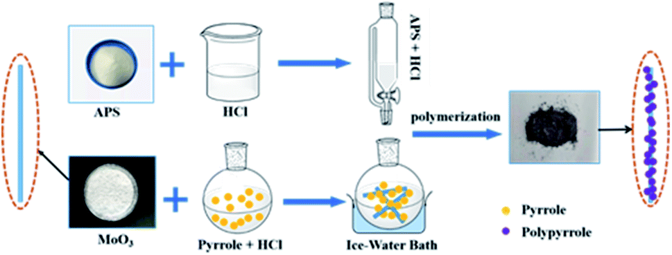
Synthesis of the MoO3@PPy nanowires
The 1D MoO3 nanowires were prepared as follows: 1.159 g of (NH4)6Mo7O24·4H2O was dissolved in 65 mL deionized water with subsequent stirring for 10 min. Next, 5 mL concentrated nitric acid was dropwise added. Keep stirring for another 20 min, the homogeneous solution was poured into Teflon-lined stainless-steel autoclave (100 mL) and reacted at 190 °C for 6 h. The resulting precipitate of MoO3 nanowires was washed for several times with DI water and absolute ethanol and finally dried at 60 °C overnight. To fabricate MoO3@PPy nanowires, 0.2 g of as-prepared MoO3 nanowires was fully dispersed into 30 mL 0.5 M HCl aqueous solution at first. Subsequently, 0.07 mL pyrrole was added into the above solution and stirred for 30 min in an ice bath. Then, 3.0 g of (NH4)2S2O8 (dissolved in 30 mL 0.5 M HCl aqueous solution) was slowly dropped into the above solution. The mixture was kept stirring at ice bath for 6 h. Finally, the obtained MoO3@PPy nanowires was washed with DI water and absolute ethanol, respectively, and then dried under vacuum at 60 °C for 12 h. The synthetic process was shown in Fig. 1. The PPy nanoparticles were synthesized through the above-mentioned process in the absence of MoO3 nanowires.
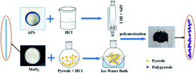 |
| | Fig. 1 Schematic illustration of the synthetic process of MoO3@PPy nanowires. | |
Synthesis of the MoO2/NC heteronanowires
To obtain 1D MoO2/NC heteronanowires, 0.9 g of the as-prepared MoO3@PPy nanowires were placed in a porcelain ware uniformly and then transferred into a tube furnace for sintering. The harvested powder was annealed at 600 °C for 3 h with a heating rate of 5 °C min−1 under N2 atmosphere. The final black products were collected for further use.
Characterization
The crystal structure was characterized by an X-ray diffractometer (Cu Kα radiation, λ = 1.5406 Å, 40 kV, 40 mA, X'Pert3 powder) in the range of 2θ = 10–80°. Fourier-transform infrared (FT-IR) absorption spectra of the samples were measured on a Nicolet iZ10 FT-IR spectrometer by the KBr method. The morphologies were observed by scanning electron microscope (SEM, FEI Quanta 250) and transmission electron microscope (TEM, JEM-2100F). The electrical conductivity of powder was measured by powder resistivity tester (ST2742B).
EMW absorption measurement
The MoO2/NC–TPU composites for EMW absorption measurement were prepared by mixing the powder with TPU matrix in a series of mass percentages. In a typical synthesis, TPU was dissolved in N,N-dimethylformamide (DMF) under ambient temperature. Keep stirring for 1 h until the solution became transparent. Subsequently, various contents of MoO2/NC heteronanowires were added to the above solution and sonicated the dispersion uniformly. Poured the mixed solution into glassy Petri dishes and then dried in an oven at 90 °C for 3 h. Finally, the dried membranes were hot compressed into rectangular-shaped samples (length: 22.86 mm, width: 10.16 mm). The complex permittivity and permeability values were determined through a vector network analyzer (VNA, E5071C, Agilent Technologies) according to waveguide method in X band.
Results and discussion
The typical XRD patterns of MoO3@PPy nanowires and MoO2/NC heteronanowires shown in Fig. 2a are readily indexed to the pure orthorhombic phase (JCPDS no. 35-0609) of MoO3 and monoclinic phase (JCPDS no. 32-0671) of MoO2, respectively. From the narrow and sharp peaks, it is confirmed that they are highly crystallized without any other impurities. Furthermore, the wide diffraction peaks existed in pristine PPy nanoparticles and MoO3@PPy nanowires indicate its amorphous structure of PPy, and proving that the MoO3 nanowires are well coated by PPy simultaneously. However, the XRD pattern of amorphous carbon is concealed by the strong diffraction intensity of MoO2. The FTIR spectra of PPy, MoO3, MoO3@PPy and MoO2/NC are depicted in Fig. 2b. Characteristic peaks at 1450 cm−1 and 1510 cm−1 correspond to the symmetric and asymmetric vibration of pyrrole ring, respectively. The peaks appear at around 934, 1050, 1372 and 1621 cm−1 are ascribed to C–N stretching vibration, N–H in-plane deformation vibration, ![[double bond, length as m-dash]](https://www.rsc.org/images/entities/char_e001.gif) C–H in plane vibration and CC stretch vibration of pyrrole ring, respectively. As to MoO3@PPy nanocomposites, distinct peaks present at 1061, 1396 and 1621 cm−1 are similar to the PPy. The slight shift of these peak is probably due to the interaction between MoO3 and PPy. Furthermore, the peaks at 996, 874 and 565 cm−1 shown in FTIR spectrum of MoO3@PPy nanowires agree well with that of MoO3 nanowires. These results are all accordance with that of the XRD. After high temperature calcination treatment, the absorption bands of NC at 1452 cm−1 and 1631 cm−1 in MoO2/NC nanocomposites are indexed to the stretching vibration of CN and CC bonds. Additionally, the peaks at 780 cm−1 and 922 cm−1 of Mo–O bond further prove the existence of MoO2.31–34
C–H in plane vibration and CC stretch vibration of pyrrole ring, respectively. As to MoO3@PPy nanocomposites, distinct peaks present at 1061, 1396 and 1621 cm−1 are similar to the PPy. The slight shift of these peak is probably due to the interaction between MoO3 and PPy. Furthermore, the peaks at 996, 874 and 565 cm−1 shown in FTIR spectrum of MoO3@PPy nanowires agree well with that of MoO3 nanowires. These results are all accordance with that of the XRD. After high temperature calcination treatment, the absorption bands of NC at 1452 cm−1 and 1631 cm−1 in MoO2/NC nanocomposites are indexed to the stretching vibration of CN and CC bonds. Additionally, the peaks at 780 cm−1 and 922 cm−1 of Mo–O bond further prove the existence of MoO2.31–34
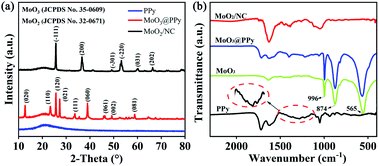 |
| | Fig. 2 (a) XRD patterns of PPy, MoO3@PPy and MoO2/NC; (b) FTIR spectra of PPy, MoO3, MoO3@PPy and MoO2/NC. | |
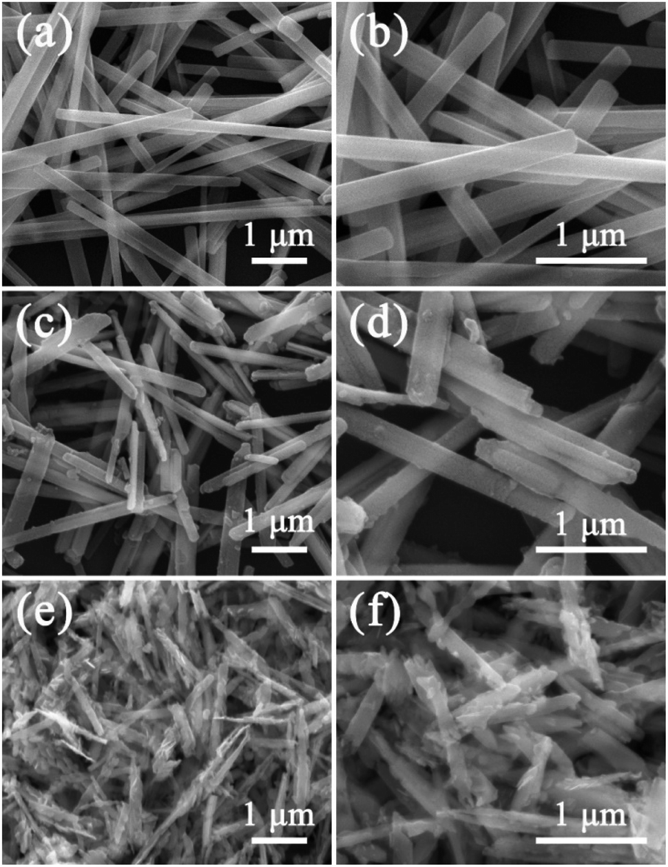
The morphology of MoO3, MoO3@PPy and MoO2/NC are investigated by SEM measurement. It is obviously observed that the prepared MoO3 presents 1D nanowires with widths of ∼300 nm and lengths of several micrometers. Moreover, their surfaces are very smooth (Fig. 3a and b). From the SEM images of MoO3@PPy displayed in Fig. 3c and d, the MoO3 nanowires are homogeneously wrapped by PPy to form core–shell structure with rough surfaces. As shown in Fig. 3e and f, all of the 1D nanostructure are fully maintained after the pyrolysis treatment, whereas the morphology has changed to a great extent. In addition, the SEM image of pristine PPy nanoparticles is exhibited in Fig. S1† for comparison. Furthermore, in order to determine how the 1D MoO2/NC heteronanowires disperse in TPU matrix, the SEM images of the fracture section of MoO2/NC–TPU membrane are displayed in Fig. S2.† It is noted that these MoO2/NC heteronanowires not only disperse well in TPU, but also maintain the 1D nanostructure.
 |
| | Fig. 3 SEM images of (a and b) MoO3 nanowires; (c and d) MoO3@PPy nanowires and (e and f) MoO2/NC heteronanowires. | |
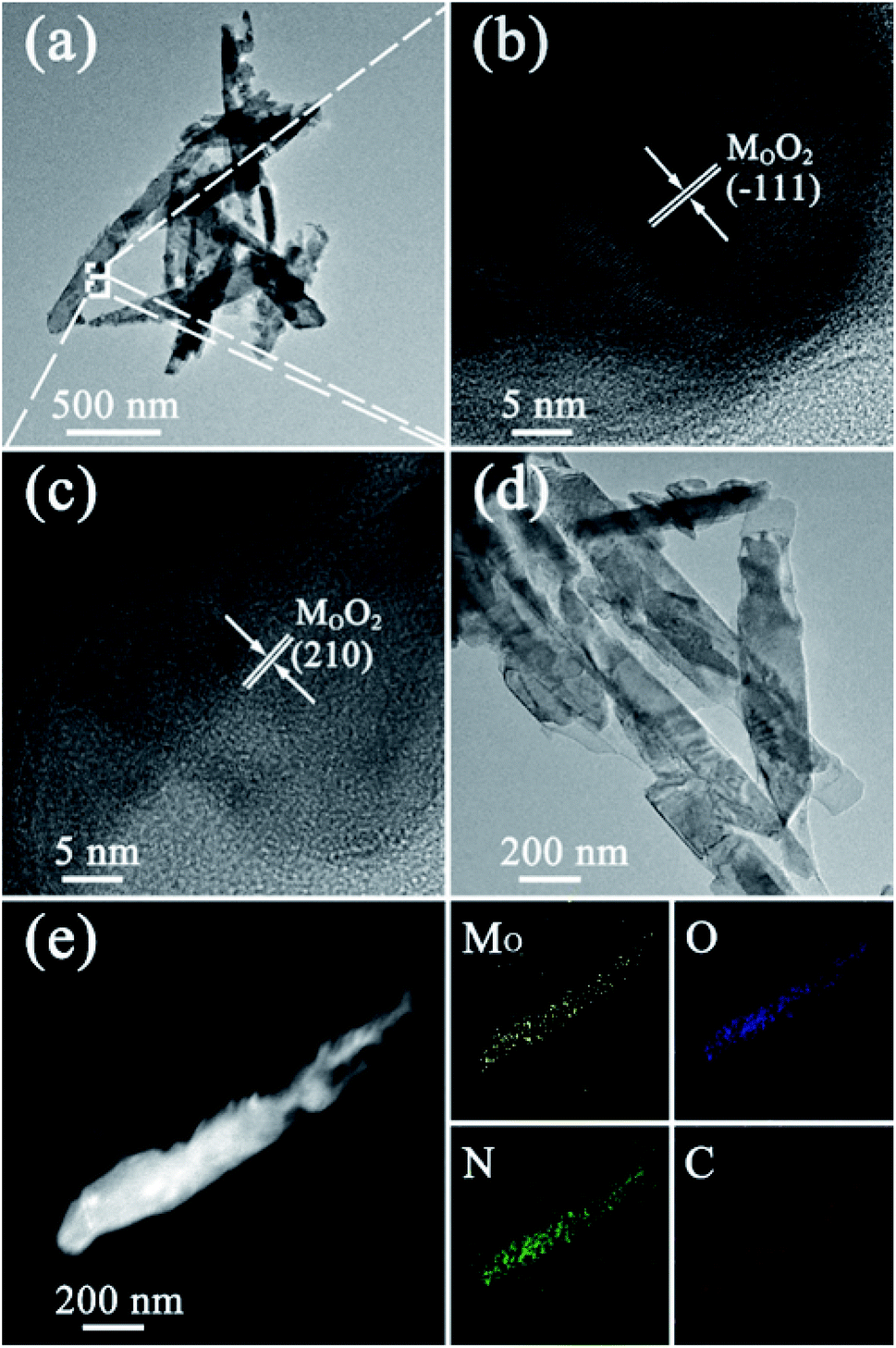
To further verify the morphology and crystal structure of 1D MoO2/NC heteronanowires, the TEM and high-resolution TEM images have been displayed in Fig. 4a–d. From the TEM images, it is obvious that the MoO2/NC nanocomposites present 1D nanowire-like heterostructure. As shown in Fig. 4b and c, the ordered lattice fringes are clearly appeared in the HRTEM images. The spacings between two neighboring lattice fringes are approximately 0.34 nm and 0.22 nm, belonging to the (−111) and (210) plane of MoO2. The amorphous structure of the outer layer refers to carbon shell. Moreover, the EDX elemental maps of MoO2/NC heteronanowire (Fig. 4e) clearly reveal a uniform distribution of Mo, O, N and C elements, which corresponds to the result of FI-TR spectrum.
 |
| | Fig. 4 (a and d) TEM images, (b and c) HRTEM images of MoO2/NC heteronanowires; (e) the elemental mappings of Mo, O, N and C. | |
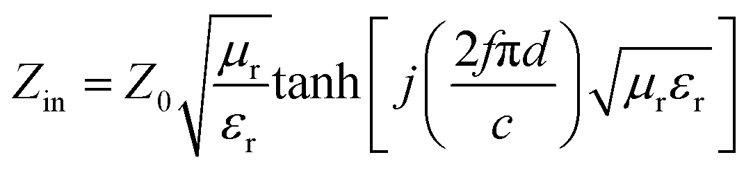
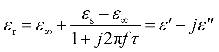
The EMW absorption properties of MoO3@PPy and MoO2/NC incorporated in TPU matrix are evaluated by RL values. On the basis of the transmission line theory, the RL values can be theoretically calculated by the following formula:35
| |
 | (1) |
| |
 | (2) |
where,
εr and
μr represent the complex permittivity and permeability of the absorber, respectively;
f is the test frequency;
d is the thickness;
c is the speed of light;
Zin is the intrinsic impedance and
Z0 is the impedance of free space.
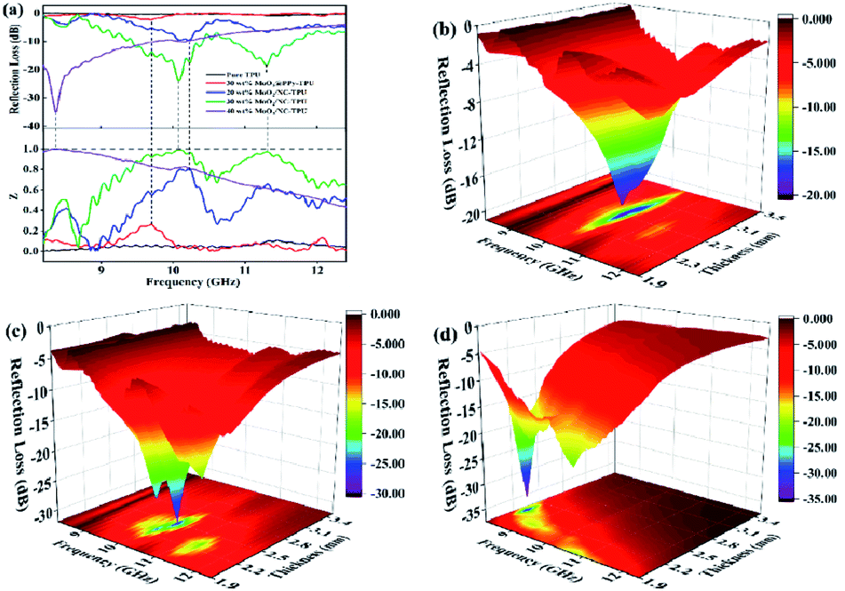
Fig. 5a displays the RL values of Pure TPU, 30 wt% MoO
3@PPy–TPU and MoO
2/NC–TPU with different filler loadings (20 wt%, 30 wt% and 40 wt%) at 2.3 mm in X-band. Generally, concentrating on the X-band is vital for an EMW absorbing material in military because the X-band is mainly applied in fire control and target-tracking radars.
36 The RL
min value of MoO
2/NC–TPU with 40 wt% loading is up to −35.0 dB at 8.37 GHz. Moreover, the EAB reaches 3.26 GHz (8.49–11.75 GHz) when the thickness is only 2.0 mm, covering almost the entire X-band (Fig. S3d
†). Interestingly, when the filler amount turns into 30 wt%, dual-absorption peaks appear with RL
min of −23.7 dB (10.09 GHz) and −18.4 dB (11.3 GHz). To explore the relationship between wave absorption property and impedance matching characteristic, the impedance matching coefficient (
Z) of these samples can be expressed as follows:
| |
 | (3) |
| |
 | (4) |
 |
| | Fig. 5 (a) Microwave RL curves of the samples with a thickness of 2.3 mm in X band. Three-dimensional representations of the RL of MoO2/NC–TPU composites with a loading of (b) 20 wt%, (c) 30 wt% and (d) 40 wt%. | |
When the value of Z approaches 1.0, it is indicated that the incident EMW enters the inner of material completely without any reflection. From the impedance matching curve in Fig. 5a, it can be seen that the optimized Z corresponds to optimal EMW attenuation capacity. Furthermore, the three-dimensional diagrams of calculated theoretical RLs of MoO2/NC–TPU with different loadings versus the frequency and thickness are displayed in Fig. 5b–d, which manifests the EMW absorbing performance among different frequencies enable to be effectively regulated by tuning the thickness and load levels of the fillers. The RL curves shown in Fig. S3† also verify this viewpoint.
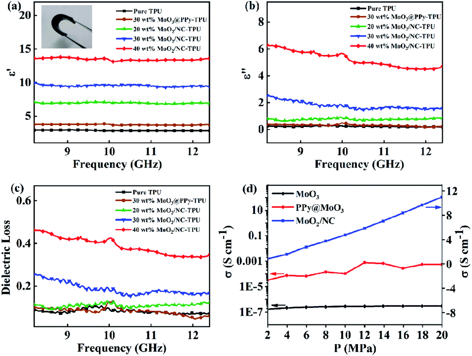
Normally, the EMW absorption behavior is desperately dependent on the relative permittivity and permeability. The related EMW absorption mechanism will be discussed by analyzing the complex permittivity (εr = ε′ − jε′′) and complex permeability (μr = μ′ − jμ′′). As is well known, the real parts ε′ and μ′ signify the storage ability under the action of an external electric and magnetic field, while the imaginary parts (ε′′ and μ′′) are relevant to the dissipation capability of electric and magnetic energy.37 Owing to the nonmagnetic MoO3@PPy and MoO2/NC nanocomposites, the complex permeability will be ignored. From Fig. 6a, it is obviously that the ε′ values of various samples almost remain constant within X band, indicating there is no occurrence of polarization lag. According to Dai' research,38 the ε′ results from the effect of conductivity and polarizations. In general, the dielectric behavior is mainly ascribed to multifarious polarizations which induced by electron, ion, interfacial, dipole and space-charge. However, the ion and electron polarization usually occur at high frequency such as PHz and THz.12 In this case, the enhancive ε′ for MoO2/NC–TPU hybrid is attributed to interfacial, dipole and space-charge polarizations. The interface generated among MoO2, N doped C and TPU will bring strong relaxation loss as a result of interfacial polarization. The N atoms in MoO2/NC heteronanowires destroy the balance of charge distribution on the original carbon lattice and act as polarized centers to generate dipolar polarization, leading to stronger dielectric loss. Additionally, the 1D structure and network are beneficial to create migration and hopping of electrons, thereby endowing space-charge polarization.39,40 In Fig. 6b, the ε′′ values of 20 wt% and 30 wt% MoO2/NC–TPU composites show a weakening trend with the increasing frequency. This can be explained by the free electron theory: ε′′ ≈ 1/2πε0ρf, where ρ is the resistivity and ε0 is the vacuum permittivity.41 This implies ε′′ is in inverse proportion to resistivity ρ. In other words, the ε′′ value is proportional to conductivity σ. Fig. 6d exhibits the σ values of MoO3, MoO3@PPy and MoO2/NC powder, which is correspond with the variation trend of ε′′ values. Obviously, the σ of MoO2/NC is much higher than that of MoO3 and MoO3@PPy due to the pyrolysis treatment. Thus, the ε′′ value of MoO2/NC–TPU composites is the highest, and it increases with the augment of filler amounts. The dielectric loss tangent (tan![[thin space (1/6-em)]](https://www.rsc.org/images/entities/char_2009.gif) δ = ε′′/ε′) delegates the wave dissipation ability of an absorber. The higher tanδ contribute to losing more EMW energy. The tanδ values of MoO2/NC–TPU composites with filler content of 30 wt% and 40wt% shown in Fig. 6c are significantly higher than that of the others, which corresponds to the above RL curves (Fig. 5a). As aforementioned, our group selects TPU as matrix to satisfy the commercial application. The photograph inserted in Fig. 6a demonstrates that the addition of MoO2/NC powder does not affect the integral flexibility of TPU-based tablet.
δ = ε′′/ε′) delegates the wave dissipation ability of an absorber. The higher tanδ contribute to losing more EMW energy. The tanδ values of MoO2/NC–TPU composites with filler content of 30 wt% and 40wt% shown in Fig. 6c are significantly higher than that of the others, which corresponds to the above RL curves (Fig. 5a). As aforementioned, our group selects TPU as matrix to satisfy the commercial application. The photograph inserted in Fig. 6a demonstrates that the addition of MoO2/NC powder does not affect the integral flexibility of TPU-based tablet.
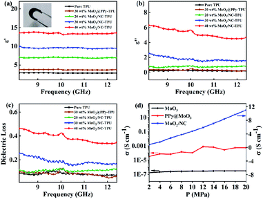 |
| | Fig. 6 Frequency dependence on (a) real, (b) imaginary part of the complex permittivity and (c) dielectric loss in X band, (d) the powder electric conductivity of different samples within 2–20 MPa. | |
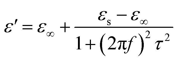
Among the polarization process, most of the EM energy is irreversibly transformed into Joule thermal energy, which is regard as the Debye relaxation theory. Based on this theory, the relative complex permittivity can be written as:42,43
| |
 | (5) |
where
f,
εs,
ε∞, and
τ represent frequency, static permittivity, relative permittivity of the frequency infinity, and polarization relaxation time, respectively. Thus,
ε′ and
ε′′ can be expressed as:
| |
 | (6) |
| |
 | (7) |
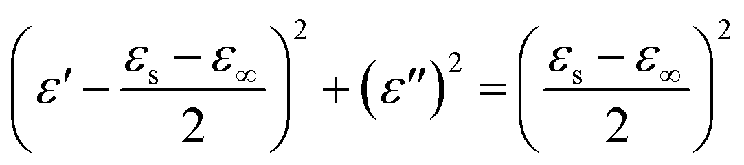
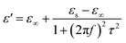
According to eqn (6) and (7), the relationship between ε′ and ε′′ are described as:
| |
 | (8) |
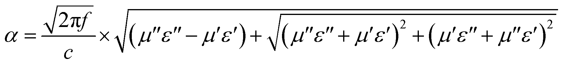
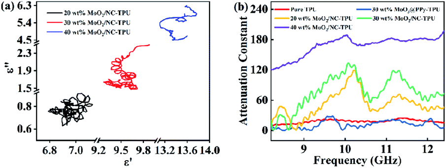
Therefore, the curve of ε′ versus ε′′ would produce a single semicircle, generally signified as the Cole–Cole semicircle.44 Each semicircle represents Debye dipolar relaxation. As depicted in Fig. 7a, there are several semicircle diagrams showing multiple Debye relaxation processes in the MoO2/NC–TPU composites, which stems from the polarization raised from heterogeneous interfaces and defects. With the fill loading increases to 30 wt% and 40 wt%, there is the upward tail appears in the curve, indicating the existence of conduction loss which caused by the formation of conductive network.17 Correspondingly, attenuation constant (α) is another key factor that should be considered for the EMW dissipation ability based on transmission line theory:45
| |
 | (9) |
 |
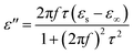
| | Fig. 7 (a) The ε′–ε′′ curves of MoO2/NC–TPU composites under different filler loadings; (b) attenuation constants of various samples. | |
Generally speaking, the larger α is inclined to bring about more dielectric loss, which is advantageous to improve wave absorption performance. Fig. 7b shows the frequency dependence of α for various samples. It is worth noted that the 40 wt% MoO2/NC–TPU composites own the highest α value among these samples in the test frequency range and it basically enlarges with the increase of frequency. Nevertheless, the RLmin does not appear at the frequency which the maximum attenuation constant occurs, demonstrating that there are some other factors such as impedance match affecting the wave absorption performance. The variation trend of the attenuation constant among other samples is almost consistent with their corresponding RL curves.
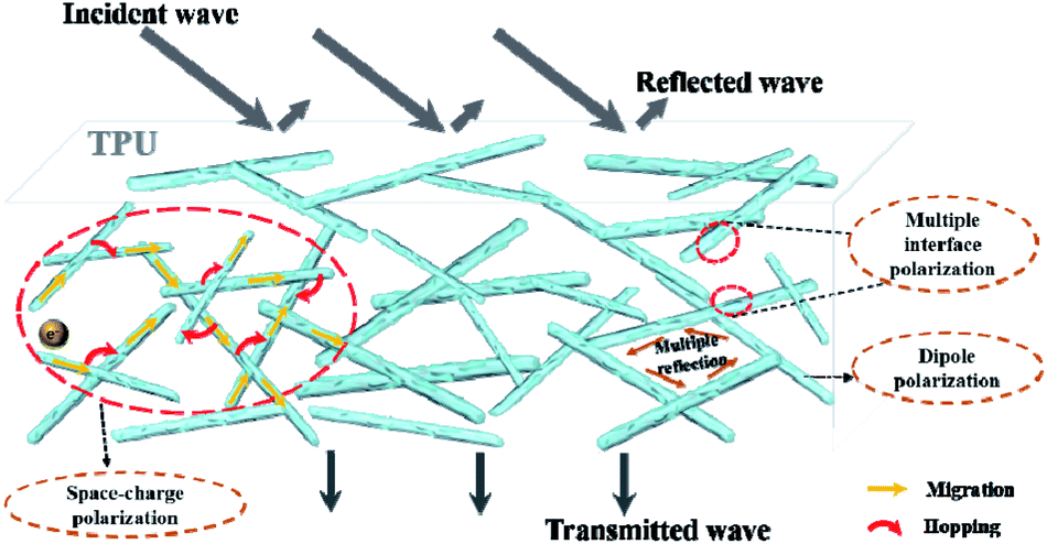
Apart from the above description, the 1D heterogeneous MoO2/NC nanowires contribute to form interconnected conductive networks in TPU matrix. The conductive networks tend to decrease the energy barrier of electron hopping and provide longer transmission path for the migration of free carriers, leading to great enhancement for conduction loss according to the Debye theory and free electron theory. On the other hand, the heterogeneous nanostructure and netlike structure contribute to offering more active sites for multiple reflection/scattering and possessing many complicated interfaces which are conducive to obtain better dielectric loss properties.10,46 The relevant wave absorption mechanism can be exhibited in Fig. 8.
 |
| | Fig. 8 The possible wave absorption mechanism of MoO2/NC–TPU composites. | |
Conclusion
In summary, the 1D MoO2/NC heteronanowires have been successfully synthesized by using MoO3 nanowires as template and then couple with in situ chemical oxidative polymerization and pyrolysis treatment. To obtain enhanced wave absorption intensity and expand practical application simultaneously, the prepared MoO2/NC absorbent was incorporated into TPU matrix to produce flexible MoO2/NC–TPU composites which could be applied in harsh environment. Owing to the dielectric loss mainly caused by dipolar/interfacial polarizations, Debye relaxation loss, as well as multiple reflection and scattering with the unique 1D heterostructure, the MoO2/NC–TPU hybrid possessed optimal microwave attenuation performance with a RLmin value of −35.0 dB at 8.37 GHz under 2.3 mm (40 wt%). Moreover, the EAB covered almost the entire X-band by tuning the thickness to 2.0 mm. In addition, when the filler amount turned into 30 wt%, dual-absorption peaks appeared with RLmin of −23.7 dB (10.09 GHz) and −18.4 dB (11.3 GHz). This work provides inspiration and insight to design and fabricate practical absorbing material with favorable performance and flexibility.
Conflicts of interest
There are no conflicts to declare.
Acknowledgements
This work was supported by the Beijing Natural Science Foundation and Key Scientific Research Project of Beijing Educational Committee (KZ202110011018), Beijing Natural Science Foundation (2214069) and Capacity building for Scientific and Technological Innovation Services-Basic Scientific Research Operating Expenses (PXM2020_014213_000017).
Notes and references
- D. Xu, N. Wu, K. Le, F. Wang, Z. Wang, L. Wu, W. Liu and A. Ouyang, J. Mater. Chem. C, 2020, 8, 2451–2459 RSC.
- X. Xu, S. Shi, Y. Tang, G. Wang, M. Zhou, G. Zhao, X. Zhou and S. Lin, Adv. Sci., 2021, 8, 2002658 CrossRef CAS PubMed.
- Y. Duan, Z. Xiao, X. Yan, Z. Gao, Y. Tang, L. Hou, Q. Li and G. Ning, ACS Appl. Mater. Interfaces, 2018, 10, 40078–40087 CrossRef CAS PubMed.
- J. Tao, J. Zhou, Z. Yao, Z. Jiao, B. Wei, R. Tan and Z. Li, Carbon, 2021, 172, 542–555 CrossRef CAS.
- Y. Wang, X. Han, P. Xu, D. Liu, L. Cui, H. Zhao and Y. Du, Chem. Eng. J., 2019, 372, 312–320 CrossRef CAS.
- L. Lyu, F. Wang, J. Qiao, X. Ding, X. Zhang, D. Xu, W. Liu and J. Liu, J. Alloys Compd., 2020, 817, 153309 CrossRef CAS.
- X. Gao, B. Wang, K. Wang, S. Xu, S. Liu, X. Liu, Z. Jia and G. Wu, J. Colloid Interface Sci., 2021, 583, 510–521 CrossRef CAS PubMed.
- Y. Cheng, W. Meng, Z. Li, H. Zhao, J. Cao, Y. Du and G. Ji, J. Mater. Chem. C, 2017, 5, 8981–8987 RSC.
- M. Han, X. Yin, Z. Hou, C. Song, X. Li, L. Zhang and L. Cheng, ACS Appl. Mater. Interfaces, 2017, 9, 11803–11810 CrossRef CAS PubMed.
- F. Wang, Y. Sun, D. Li, B. Zhong, Z. Wu, S. Zuo, D. Yan and R. Zhuo, Carbon, 2018, 134, 264–273 CrossRef CAS.
- Q. Wang, Z. Lei, Y. Chen, Q. Ouyang, P. Gao, L. Qi, C. Zhu and J. Zhang, J. Mater. Chem. A, 2013, 1, 11795–11801 RSC.
- L. Liang, G. Han, Y. Li, B. Zhao, B. Zhou, Y. Feng, J. Ma and Y. Wang, ACS Appl. Mater. Interfaces, 2019, 11, 25399–25409 CrossRef CAS PubMed.
- C. Song, X. Yin, M. Han, X. Li, Z. Hou, L. Zhang and L. Cheng, Carbon, 2017, 116, 50–58 CrossRef CAS.
- G. Wang, Z. Gao, S. Tang, C. Chen, F. Duan, S. Zhao, S. Lin and Y. Feng, ACS Nano, 2012, 6, 11009–11017 CrossRef CAS PubMed.
- Y. Gong, L. Zhen, J. Jiang, C. Xu, W. Wang and W. Shao, CrystEngComm, 2011, 13, 6839–6844 RSC.
- S. Dong, W. Tang, P. Hu, X. Zhao, X. Zhang, J. Han and P. Hu, ACS Sustainable Chem. Eng., 2019, 7, 11795–11805 CrossRef CAS.
- H. Zhang, C. Shi, Z. Jia, X. Liu, B. Xu, D. Zhang and G. Wu, J. Colloid Interface Sci., 2021, 584, 382–394 CrossRef CAS PubMed.
- Y. Tong, M. He, Y. Zhou, S. Nie, X. Zhong, L. Fan, T. Huang and Q. Liao, ACS Sustainable Chem. Eng., 2018, 6, 8212–8222 CrossRef CAS.
- W. You, H. Bi, W. She, Y. Zhang and R. Che, Small, 2017, 13, 1602779 CrossRef PubMed.
- Y. Wang, D. Li, X. Han, P. Xu, L. Cui, H. Zhao, D. Liu and F. Wang, Chem. Eng. J., 2020, 387, 124159 CrossRef CAS.
- D. Xu, J. Qiao, N. Wu, W. Liu, F. Wang, L. Lv, J. Pan and Y. Dong, ACS Sustainable Chem. Eng., 2019, 7, 8687–8695 CrossRef CAS.
- E. Zhou, C. Wang, M. Shao, X. Deng and X. Xu, Ceram. Int., 2017, 43, 760–765 CrossRef CAS.
- X. Han, C. Gerke, S. Banerjee, M. Zubair, J. Jiang, N. Bedford, E. Miller and V. Thoi, ACS Energy Lett, 2020, 5, 3237–3243 CrossRef CAS.
- Y. Zhang, S. Yang, S. Wang, H. Liu, L. Li, S. Dou and X. Liu, Small, 2018, 14, 1800480 CrossRef PubMed.
- L. Bai, C. Wu, G. Lai, Y. Zhu, L. Dong and Z. Zhang, Mater. Lett., 2018, 228, 203–206 CrossRef CAS.
- Z. Song, X. Liu, X. Sun, Y. Li, X. Nie, W. Tang, R. Yu and J. Shui, Carbon, 2019, 151, 36–45 CrossRef CAS.
- P. Liu, Y. Zhang, J. Yan, Y. Huang, L. Xia and Z. Guang, Chem. Eng. J., 2019, 368, 285–298 CrossRef CAS.
- C. Zhou, S. Geng, X. Xu, T. Wang, L. Zhang, X. Tian, F. Yang and H. Yang, Carbon, 2016, 108, 234–241 CrossRef CAS.
- J. Zhou, X. Wang, K. Ge, Z. Yang, H. Li, C. Guo, J. Wang, Q. Shan and L. Xia, J. Colloid Interface Sci., 2022, 607, 881–889 CrossRef CAS PubMed.
- P. Gahlout and V. Choudhary, Synth. Met., 2020, 266, 116414 CrossRef CAS.
- L. Gai, Y. Zhao, G. Song, Q. An, Z. Xiao, S. Zhai and Z. Li, Composites, Part A, 2020, 136, 105965 CrossRef CAS.
- X. Zhang, X. Zeng, M. Yang and Y. Qi, ACS Appl. Mater. Interfaces, 2014, 6, 1125–1130 CrossRef CAS PubMed.
- X. Wu, Q. Wang, W. Zhang, Y. Wang and W. Chen, Mater. Lett., 2016, 182, 121–124 CrossRef CAS.
- Y. Yun, Z. Shi, J. Shao, Q. Qu, Y. Gao, Z. Chen, Y. Chen and H. Zheng, ChemNanoMat, 2018, 4, 1247–1253 CrossRef CAS.
- L. Liu, S. Zhang, F. Yan, C. Li, C. Zhu, X. Zhang and Y. Chen, ACS Appl. Mater. Interfaces, 2018, 10, 14108–14115 CrossRef CAS PubMed.
- L. Liang, R. Yang, G. Han, Y. Feng, B. Zhao, R. Zhang, Y. Wang and C. Liu, ACS Appl. Mater. Interfaces, 2020, 12, 2644–2654 CrossRef CAS PubMed.
- B. Zhao, X. Guo, Y. Zhou, T. Su, C. Ma and R. Zhang, CrystEngComm, 2017, 19, 2178–2186 RSC.
- S. Dai, Y. Cheng, B. Quan, X. Liang, W. Liu, Z. Yang, G. Ji and Y. Du, Nanoscale, 2018, 10, 6945–6953 RSC.
- P. Liu, S. Gao, Y. Wang, Y. Huang, Y. Wang and J. Luo, ACS Appl. Mater. Interfaces, 2019, 11, 25624–25635 CrossRef CAS PubMed.
- L. Liang, Z. Liu, L. Xie, J. Chen, H. Jia, Q. Kong, G. Sun and C. Chen, Carbon, 2021, 171, 142–153 CrossRef CAS.
- H. Lv, Y. Guo, G. Wu, G. Ji, Y. Zhao and Z. Xu, ACS Appl. Mater. Interfaces, 2017, 9, 5660–5668 CrossRef CAS PubMed.
- X. Zhang, G. Wang, W. Cao, Y. Wei, M. Cao and L. Guo, RSC Adv., 2014, 4, 19594–19601 RSC.
- J. Yan, Y. Huang, X. Han, X. Gao and P. Liu, Composites Part B, 2019, 163, 67–76 CrossRef CAS.
- X. Hong, Q. Wang, Z. Tang, W. Khan, D. Zhou and T. Feng, J. Phys. Chem. C, 2015, 120, 148–156 CrossRef.
- X. Zhang, J. Zhu, P. Yin, A. Guo, A. Huang, L. Guo and G. Wang, Adv. Funct. Mater., 2018, 28, 1800761 CrossRef.
- Z. Cai, L. Su, H. Wang, M. Niu, H. Gao, D. Lu and M. Li, ACS Appl. Mater. Interfaces, 2020, 12, 8555–8562 CrossRef CAS PubMed.
Footnote |
| † Electronic supplementary information (ESI) available. See DOI: 10.1039/d1ra09074g |
|
| This journal is © The Royal Society of Chemistry 2022 |
Click here to see how this site uses Cookies. View our privacy policy here. 
 Open Access Article
 This Open Access Article is licensed under a Creative Commons Attribution-Non Commercial 3.0 Unported Licence
 and
Bianying Wen
and
Bianying Wen