
 Open Access Article
 This Open Access Article is licensed under a Creative Commons Attribution-Non Commercial 3.0 Unported Licence
Interfacial carrier transport properties of a gallium nitride epilayer/quantum dot hybrid structure†
Huiyun Wei acd,
Peng Qiua,
Meina Yub,
Yimeng Songa,
Ye Lia,
Yingfeng Hea,
Mingzeng Penga,
Xiaohu Liu*cd and
Xinhe Zheng*a
acd,
Peng Qiua,
Meina Yub,
Yimeng Songa,
Ye Lia,
Yingfeng Hea,
Mingzeng Penga,
Xiaohu Liu*cd and
Xinhe Zheng*a
aBeijing Advanced Innovation Center for Materials Genome Engineering, Beijing Key Laboratory for Magneto-Photoelectrical Composite and Interface Science, School of Mathematics and Physics, University of Science and Technology Beijing, Beijing, 100083, PR China. E-mail: xinhezheng@ustb.edu.cn
bInstitute for Advanced Materials and Technology, University of Science and Technology Beijing, Beijing, 100083, PR China
cSchool of Biomedical Engineering, School of Ophthalmology & Optometry, Wenzhou Medical University, Wenzhou 325027, PR China. E-mail: liuxiaohu@wmu.edu.cn
dEngineering Research Center of Clinical Functional Materials and Diagnosis & Treatment Devices of Zhejiang Province, Wenzhou Institute, University of Chinese Academy of Sciences (Wenzhou Institute of Biomaterials & Engineering), Wenzhou 325027, PR China
First published on 17th January 2022
Abstract
Electron transport layers (ETLs) play a key role in the electron transport properties and photovoltaic performance of solar cells. Although the existing ETLs such as TiO2, ZnO and SnO2 have been widely used to fabricate high performance solar cells, they still suffer from several inherent drawbacks such as low electron mobility and poor chemical stability. Therefore, exploring other novel and effective electron transport materials is of great importance. Gallium nitride (GaN) as an emerging candidate with excellent optoelectronic properties attracts our attention, in particular its significantly higher electron mobility and similar conduction band position to TiO2. Here, we mainly focus on the investigation of interfacial carrier transport properties of a GaN epilayer/quantum dot hybrid structure. Benefiting from the quantum effects of QDs, suitable energy level arrangements have formed between the GaN and CdSe QDs. It is revealed that the GaN epilayer exhibits better electron extraction ability and faster interfacial electron transfer than the rutile TiO2 single crystal. Moreover, the corresponding electron transfer rates of 4.44 × 10⁸ s−1 and 8.98 × 10⁸ s−1 have been calculated, respectively. This work preliminarily shows the potential application of GaN in quantum dot solar cells (QDSCs). Carefully tailoring the structure and optoelectronic properties of GaN, in particular realizing the low-temperature deposition of high-quality GaN on various substrates, will significantly promote the construction of highly efficient GaN-ETL based QDSCs.
1. Introduction
Quantum dots (QDs) with fascinating optoelectronic properties have shown potential applications in photovoltaic devices. In particular in the past five years, quantum dot solar cells (QDSCs) containing conventional chalcogenide QDs or halide perovskite QDs have experienced rapid development. The progress in developing new QD materials and achieving high-quality QD films or high QD loading has significantly improved the performance of QDSCs. Zhong's group has reported the Zn–Cu–In–S–Se based quantum dot sensitized solar cells with an excellent power conversion efficiency (PCE) over 15%,1 while perovskite solar cells (PSCs) with Cs1−xFAxPbI3 (FA = CH(NH2)2+) QDs have achieved the current highest certified PCE of 16.6%.2 On the other hand, improving the properties of electron transport layers (ETLs) is also very important due to their critical role in electron extraction and transport in devices. There are a few effective electron transport materials including wide-bandgap metal oxides such as TiO2, ZnO and SnO2, as well as fullerene and its derivatives such as phenyl-C61-butyric acid methyl ester (PCBM), that have been used in photovoltaic devices, of which the mostly studied in QDSCs remains TiO2.3 However, TiO2 has several inherent drawbacks typically including low electron mobility, high defect state density and poor chemical stability, which might result in charge accumulation at interface, and thus imbalanced electron/hole flux and unpredicted current–voltage hysteresis.4–6 For QDSCs, studies on other novel ETLs are still lacking. Exploring novel ETLs as potential alternatives which enable suitable energy level alignment, rapid interface carrier extraction and good chemical stability for QDSCs is urgently expected.Gallium nitride (GaN) is a direct bandgap semiconductor (∼3.4 eV) with good chemical stability and high theoretically calculated electron mobility (∼1000 cm2 V−1 s−1), as well as similar conduction band position to the widely-used TiO2. Meanwhile, its transmittance exceeds 80% over the entire visible wavelengths, showing the potential as an electron transport material.7 High-quality undoped or n-type doped GaN wafers have been maturely prepared by molecular beam epitaxy,8 metal–organic vapor phase epitaxy,9 hydride vapor phase epitaxy.10 Recently, our group successfully achieved the low-temperature growth of single-crystalline GaN film by plasma-enhanced atomic layer deposition (PEALD) technology.11 This low-temperature deposition promoted the photovoltaic application of GaN. We introduced the PEALD-GaN thin film into PSCs as a ETL for the first time, as a result, significantly enhanced device efficiency was achieved compared to the ETL-free device.12 Afterward, we further carefully regulated the bandgap of the PEALD-GaN films to form better energy level matching between the GaN and photoactive layer13 Kang et al. proposed a nanostructured GaN–TiO2 ETL for dye-sensitized solar cells, in which the GaN layer simultaneously promoted electron injection and prevented back electron transfer.14 Wang et al. presented a theoretical investigation on the perovskite piezo-phototronic solar cells with a GaN ETL, revealing that enhanced device performance could be realized due to the piezo-phototronic effect of GaN.15 Lee et al. designed a nanoporous GaN/n-type GaN structure for PSCs as both the transparent conductive layer and ETL, resulting in a PCE of 18.79%.16 So far, there is very limited works on GaN ETL-based solar cells, especially no report on the application of GaN in QDSCs.
In this work, the interfacial carrier transport property of GaN/QDs was investigated for the first time. Commercial n-type Si-doped GaN epilayer on sapphire substrate was selected due to its high electron mobility, as well as getting rid of the influence of grain boundary on charge transport. Meanwhile, CdSe was chosen as a representative QD material. The structure and optoelectronic properties of the GaN epilayer were firstly characterized by grazing incidence X-ray diffraction (GIXRD), atomic force microscope (AFM), Hall effect measurement, UV-Vis absorption and ultraviolet photoelectron spectroscopy (UPS). Subsequently, the interfacial electron transport of the GaN/CdSe and TiO2/CdSe samples was compared using both steady-state photoluminescence (PL) and time-resolved PL (TRPL). Benefiting from the quantum effects of QDs, suitable energy level arrangements were easier to form for GaN/QDs. It was revealed that the GaN epilayer exhibited better electron extraction ability and faster electron transfer than that of the rutile TiO2 single crystal. The corresponding electron transfer rates were calculated to be 4.44 × 10⁸ s−1 and 8.98 × 10⁸ s−1, respectively. This work has paved the way for the potential application of GaN in QDSCs. Carefully tailoring the structure and optoelectronic properties of GaN, especially realizing the low-temperature deposition of high-quality GaN on various substrates (such as transparent conductive substrate) will significantly promote the construction of high efficient GaN-ETL based QDSCs.
2. Experimental
2.1 Fabrication of the GaN/CdSe and TiO2/CdSe hybrid structures
Oleylamine (OAm) ligand-capped CdSe (OAm-CdSe) colloidal QDs were synthesized by hot-injection method according the previous literature.17 CdSe QDs with different sizes were obtained by controlling injection temperature. After purification with methanol and acetone, the as-prepared CdSe QDs were redispersed into octane. N-type Si-doped GaN epilayer on sapphire (diameter: 50.8 ± 0.5 mm, thickness: 4.5 ± 0.5 μm) was purchased from Homray Material Technology Co., Ltd, which was cleaned in ultrasonic bath with acetone and ethanol successively. As a contrast, rutile TiO2 single crystal with (100) orientation was also employed, which was purchased from Hefei Kejing Co., Ltd, and cleaned using the same method. CdSe QD films were deposited on the above GaN and TiO2 surface through successively spin-coating the CdSe QDs solution (50 mg ml−1) at 1500 rpm for 10 s and 5000 rpm for 30 s. Then, a ligand exchange to replace the OAm ligand with thioglycolic acid (TGA) was performed. In detail, a solution comprising 2.0 mmol TGA and 10 ml methanol was dropped on the OAm-CdSe QD film and soaked for 30 s, then spin coated at 5000 rpm for 30 s. To eliminate the residual reactants, the film was washed twice by flooding surface with methanol for 10 s before spin-coating dry at 5000 rpm for 30 s. The above deposition-ligand exchange-washing process was repeated four times to produce CdSe films with thickness of ∼150 nm.2.2 Characterization
The crystallization characteristic and morphology of the GaN epilayer were measured by GIXRD (Smartlab) and AFM (Bruker Dimension ICON), respectively. The valence band spectrum was obtained by UPS (Thermo ESCALAB 250XI PHI5000 VersaProbe III with the He I laser source (hν = 21.20 eV) at room temperature). UV-Vis absorption spectra were measured using a UV-Vis spectrophotometer (LAMBDA 950). Electrical properties of both the GaN epilayer and TiO2 single crystal were determined from Hall measurement (Ecopia HMS-7000). Steady-state PL and TRPL spectroscopy were recorded by a PL spectrometer (Edinburgh Instruments, FLS 900) with a pulsed diode laser (EPL-445, 0.8 μJ cm−2).3. Result and discussion
3.1 Structure and optoelectronic properties of the GaN epilayer
Herein, Si-doped n-type GaN epilayer on sapphire substrate was chosen to study the electron extraction property, as it had high electron mobility and the advantage to avoid the interference from high number of grain boundaries. Before fabricating GaN/QD hybrid structure, the basic properties of the GaN epilayer were charactered. From the GIXRD spectrum presented in Fig. 1(a), the diffraction peaks at 34.74° and 72.98° were obviously distinguished, which could be straightforwardly assigned as the (002) and (004) plane of hexagonal GaN, respectively,18 while the diffraction peak located at 41.68° corresponded to the Al2O3 (006) of sapphire substrate. Besides, according to the AFM result (inset of Fig. 1(a)), the 4.5 μm-thick GaN layer showed smooth surface morphology with a root-mean-square (RMS) roughness of ∼1.2 Å. UV-Vis absorption spectra of the GaN was shown in Fig. 1(b). The Tauc plot was further made to estimate the bandgap (Eg) value using absorption coefficient (α) data (inset of Fig. 1(b)), and Eg = 3.39 eV was deduced. After deducting the influence of the sapphire substrate, the absolute average optical transmittance was estimated to be 86% in the visible range derived from the transmittance spectra shown in Fig. 1(c). Interestingly, there were two obvious characteristic regions in the transmittance spectra: (i) a straight line region shorter than the cut-off wavelength of ∼366 nm, (ii) an oscillation pattern afterwards. This periodic oscillation could be reasonably attributed to superposition of the multiple interference that occurred at the clear semiconductor (GaN)–insulator (Al2O3) interface, especially for the micron-thick GaN film.19 | ||
| Fig. 1 The structure and optical properties of the GaN epilayer: (a) GIXRD pattern; (b) UV-Vis absorption spectra; (c) transmittance spectra. Inset of (a) is the AFM image (size: 1 μm × 1 μm), inset of (b) is plots of (αhν)1/2 vs. photon energy hν, where α is absorption coefficient, h is Planck's constant, ν is photon frequency. | ||
As the electron transport material for photovoltaic devices, the electrical characteristics of the GaN epilayer were vitally important. Their electrical parameters were determined from Hall effect measurements, and the measured resistivity is 2.56 × 10⁻³ Ω cm. Moreover, the electron mobility and charge carrier density were 376.5 cm2 V−1 s−1 and 2.68 × 1018 cm−3, respectively. In order to facilitate the next research, the electrical properties of TiO2 were also characterized by Hall measurement for comparison. Specifically, the purchased rutile TiO2 single crystal with orientation of (100) was adopted based on our previous study.21 Unfortunately, its Hall mobility was almost impossible to measure due to the high resistivity,22,23 which usually below 10 cm2 V−1 s−1 at room temperature according to literatures.24,25 Therefore, it can be reasonably inferred that the GaN epilayer exhibits significantly higher mobility than the TiO2 single crystal.
UPS measurement was further performed to analyze the band structure. The work function (WF) of the GaN was determined from the secondary electron cutoff of UPS spectra as shown in Fig. 2(a). The WF value of 4.83 eV was deduced by calculating the difference between the cut-off energy (16.37 eV) and incident photon energy (21.20 eV). The valence band maximum (VBM) from the Fermi level (EF − VBM = 2.62 eV) is shown in Fig. 2(b), so the position of VBM was deduced to be −7.45 eV. The conduction band minimum (CBM) position of the GaN is further calculated to be −4.06 eV according to formula CBM = VBM − Eg as well as its Eg value of 3.39 eV. Similarly, the WF, VBM and CBM values of the TiO2 are respectively calculated to be 5.02, −7.25 and −4.18 eV from the UPS results (Fig. 2(c) and (d)). Clearly, the GaN epilayer exhibits slight higher conduction band position and WF than that of the rutile TiO2 single crystal. As we know, a lower WF and CBM can facilitate interfacial electron transfer and transport for ETLs.20
 | ||
| Fig. 2 UPS spectra of the (a), (b) GaN epilayer and (c), (d) TiO2 single crystal. | ||
3.2 Interfacial electron transport properties of the GaN/QD hybrid structure
CdSe colloidal QDs with different sizes were synthesized by hot injection method for constructing GaN/QD heterojunction structure. Characteristic measurements for the CdSe QDs were firstly performed, as shown in Fig. 3. Homogeneous monodisperse CdSe QDs could be confirmed by TEM (Fig. 3(a)). Meanwhile, the lattice spacing of 0.374 nm could be calculated from the HRTEM image (Fig. 3(b)), corresponding well to the (100) plane of hexagonal CdSe (JCPDS card no. 08-0459). Three different sizes of CdSe QDs with absorption edge wavelength of 571, 595 and 616 nm had been chosen. Their absorption and normalized PL emission spectra were provided in Fig. 3(c) and (d), respectively. | ||
| Fig. 3 Characteristics of CdSe QDs: (a) and (b) TEM images, scale bars: 50 nm and 5 nm, respectively; (c) UV-Vis absorption spectra and (d) normalized PL remission spectra of the three CdSe QDs. | ||
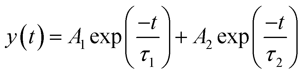
QD films were then deposited on the surface of GaN and TiO2 by spin coating the as-prepared colloidal CdSe QD solutions (50 mg ml−1). During the deposition process, in order to enhance the carrier transport within QD films, a ligand-exchange step was carried out through replacing OA with TGA ligand on the surface of CdSe QDs. As a reference, the sapphire/CdSe sample was also prepared. Steady-state PL spectra could be employed to understand the carrier transport process between GaN and CdSe QDs. As shown in Fig. 4(a), a more evident PL quenching is observed for the GaN/CdSe sample as compared with both the sapphire/CdSe and TiO2/CdSe samples, indicating an effective electron extraction from CdSe QD to the GaN.26 As shown in Fig. 4(b), TRPL decay traces were further measured to analyze the interface electron transfer properties of the GaN/CdSe samples. Consistent with our previous work,27 a bi-exponential function (eqn (1)) was found to be satisfactory in fitting these decay curves and determining the electron lifetimes.
 | (1) |
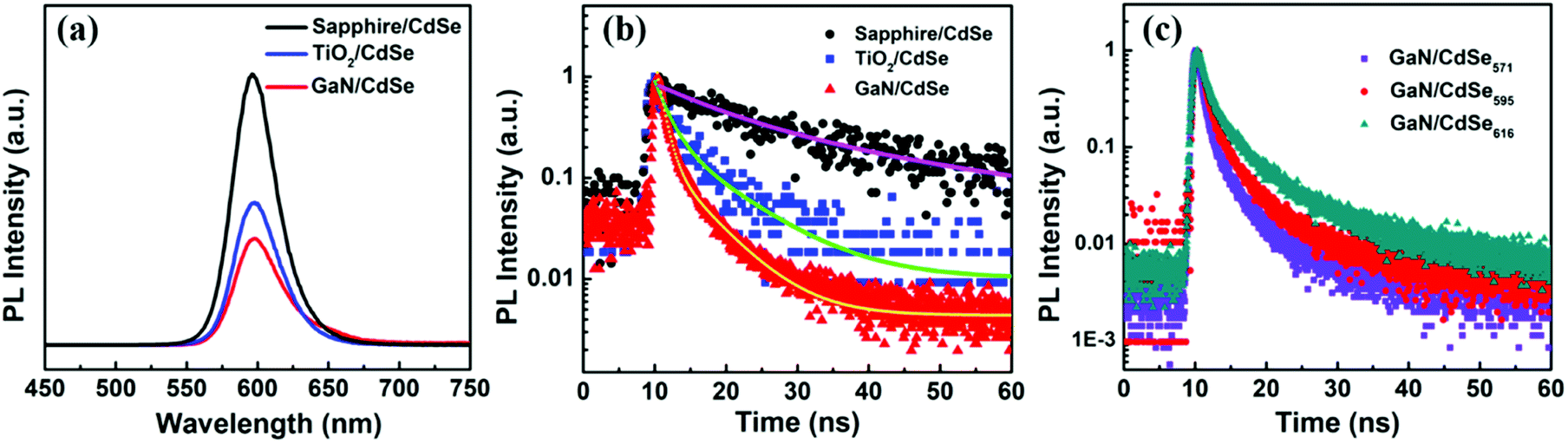 | ||
| Fig. 4 (a) Steady-state PL spectra and (b) TRPL decay traces of the CdSe QD films on bare sapphire substrate, rutile TiO2 single crystal, and GaN epilayer, respectively (in Fig. 2(b), the scatters represent experimental data, while the solid lines are fitted results). (c) TRPL decay traces of the GaN/CdSe571, GaN/CdSe595 and GaN/CdSe617 samples. | ||
| Sample | τ1 (ns) | A1 | τ2 (ns) | A2 | τave (ns) | Ket (s−1) |
|---|---|---|---|---|---|---|
| Sapphire/CdSe | 8.642 | 0.443 | 26.444 | 0.404 | 21.75 | — |
| TiO2/CdSe | 1.785 | 0.848 | 8.041 | 0.273 | 5.49 | 4.44 × 10⁸ |
| GaN/CdSe | 0.986 | 1.233 | 5.426 | 0.165 | 2.87 | 8.98 × 10⁸ |
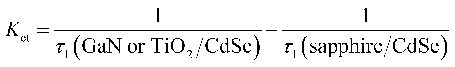
As we know, the shorter lifetime (τ1) reflected both the nonradiative recombination and electron transfer. While, the longer lifetime (τ2) described the carrier recombination in bulk materials.28 The τ1 values of the GaN/CdSe and TiO2/CdSe samples were estimated to be 2.87 and 5.49 ns, respectively, revealing the GaN epilayer enabled a faster electron extraction. The electron transfer rates (Ket) were determined to be 8.98 × 10⁸ s−1 for GaN/CdSe and 4.44 × 10⁸ s−1 for TiO2/CdSe based on the eqn (2).29 In fact, the lower conduction band position and work function of the TiO2 could facilitate interfacial electron transfer as compared with GaN. The better electron extraction ability for the GaN epilayer might be attributed to the significantly higher electron mobility and better conductivity which facilitated faster electron transport and avoided interfacial charge accumulation.
 | (2) |
Furthermore, energy level alignment dependent interfacial carrier transport between the GaN and QDs was also investigated by employing the CdSe QDs with different sizes. The energy level position of these CdSe QDs were determined by combining their UV-Vis absorption spectra (Fig. 3(c)) and UPS results (Fig. S1†). The corresponding energy band diagram was presented in Fig. 5. A typical type-II energy level alignment was formed between the GaN and CdSe QDs. The conduction band position of CdSe QDs gradually moved upward with the decrease of size, which could provide enhanced driving force for electron injection from QD to GaN. It was confirmed by the TRPL measurement as shown in Fig. 4(c) that the GaN/CdSe571 sample showed the fastest decay rate as expected.
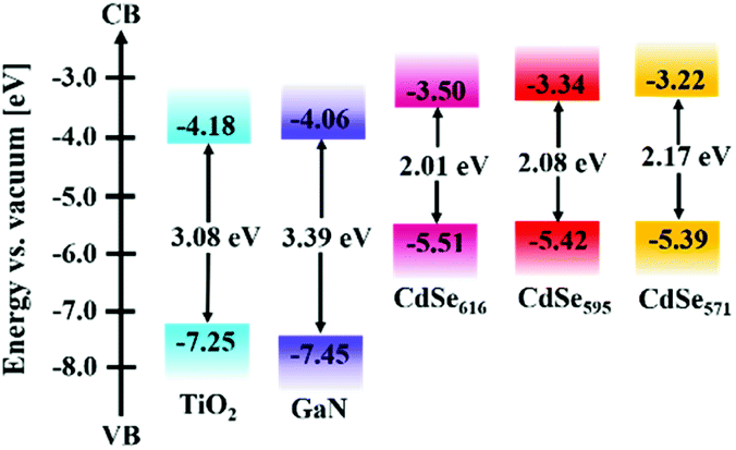 | ||
| Fig. 5 Energy level diagram of the TiO2, GaN, and CdSe QDs. | ||
4. Conclusions
In this work, the interface electron transfer of GaN/QDs has been investigated by employing the Si-doped n-GaN epilayer on sapphire, and utilizing CdSe as a representative QD material. According to the UPS results, the energy level arrangement was matched between the GaN and CdSe QDs. Both the steady state PL spectra and TRPL decay traces revealed that the GaN epilayer achieved faster electron extraction than the rutile TiO2 single crystal, which could be reasonably attributed to the significantly higher electron mobility and better conductivity. The corresponding electron injection rates for the GaN/CdSe and TiO2/CdSe samples were 8.98 × 10⁸ s−1 and 4.44 × 10⁸ s−1, respectively. As expected, the decrease of QD size resulted in the broadening of band gap and the upward shift of conduction band position due to quantum size effect, which facilitated faster electron injection from QD to GaN as well as more matched energy level alignment between GaN and QD. The above results presented the potential application of GaN in QDSCs. Transferring the GaN layer on conductive substrate or directly depositing high-quality GaN layer on transparent conductive substrate, as well as tailoring its morphology, surface area and optoelectrical properties will be the direction of future efforts for fabricating high-efficient GaN-ETL based QDSCs.Conflicts of interest
There are no conflicts to declare.Acknowledgements
This work was supported by the National Natural Science Foundation of China (Grant No. 52002021), Fundamental Research Funds for the Central Universities (Grant No. FRF-TP-20-016A2, FRF-IDRY-20-037), National Key Research and Development Program of China (2018YFA0703700), Engineering Research Center of Clinical Functional Materials and Diagnosis & Treatment Devices of Zhejiang Province (Grant No.: WIUCASK20005).Notes and references
- H. Song, Y. Lin, Z. Zhang, H. Rao, W. Wang, Y. Fang, Z. Pan and X. Zhong, J. Am. Chem. Soc., 2021, 143, 4790–4800 CrossRef CAS PubMed
.
- M. Hao, Y. Bai, S. Zeiske, L. Ren, J. Liu, Y. Yuan, N. Zarrabi, N. Cheng, M. Ghasemi, P. Chen, M. Lyu, D. He, J.-H. Yun, Y. Du, Y. Wang, S. Ding, A. Armin, P. Meredith, G. Liu, H.-M. Cheng and L. Wang, Nat. Energy, 2020, 5, 79–88 CrossRef CAS
- S. Zheng, G. Wang, T. Liu, L. Lou, S. Xiao and S. Yang, Sci. China: Chem., 2019, 62, 800–809 CrossRef CAS
- L. Zhu, X. Shang, K. Lei, C. Wu, S. Zheng, C. Chen and H. Song, Sol. RRL, 2021, 5, 2000605 CrossRef CAS
- W. Hu, S. Yang and S. Yang, Trends Chem., 2020, 2, 148–162 CrossRef CAS
- P. Tiwana, P. Docampo, M. B. Johnston, H. J. Snaith and L. M. Herz, ACS Nano, 2011, 5, 5158–5166 CrossRef CAS PubMed
- H. Zhou, J. Mei, M. Xue, Z. Song and H. Wang, J. Phys. Chem. C, 2017, 121, 21541–21545 CrossRef CAS
- X. Wang and A. Yoshikawa, Prog. Cryst. Growth Charact., 2004, 48–49, 42–103 CrossRef
- P. Gibart, Rep. Prog. Phys., 2004, 67, 667 CrossRef CAS
- M. Bockowski, M. Iwinska, M. Amilusik, M. Fijalkowski, B. Lucznik and T. Sochacki, Semicond. Sci. Technol., 2016, 31, 093002 CrossRef
- S. Liu, G. Zhao, Y. He, Y. Li, H. Wei, P. Qiu, X. Wang, X. Wang, J. Cheng, M. Peng, F. Zaera and X. Zheng, Appl. Phys. Lett., 2020, 116, 211601 CrossRef CAS
- H. Wei, J. Wu, P. Qiu, S. Liu, Y. He, M. Peng, D. Li, Q. Meng, F. Zaera and X. Zheng, J. Mater. Chem. A, 2019, 7, 25347–25354 RSC
- P. Qiu, H. Wei, Y. An, Q. Wu, W. Du, Z. Jiang, L. Zhou, C. Gao, S. Liu, Y. He, Y. Song, M. Peng and X. Zheng, Ceram. Int., 2020, 46, 5765–5772 CrossRef CAS
- B. K. Kang, Y. H. Song, S. M. Kang, Y. C. Choi, D. K. Lee, S.-W. Kim and D. H. Yoon, J. Electrochem. Soc., 2011, 158, H693–H696 CrossRef CAS
- Y. Wang, D. Zheng, L. Li and Y. Zhang, ACS Appl. Energy Mater., 2018, 1, 3063–3069 CrossRef CAS
- K. J. Lee, J.-W. Min, B. Turedi, A. Y. Alsalloum, J.-H. Min, Y. J. Kim, Y. J. Yoo, S. Oh, N. Cho, R. C. Subedi, S. Mitra, S. E. Yoon, J. H. Kim, K. Park, T.-H. Chung, S. H. Jung, J. H. Baek, Y. M. Song, I. S. Roqan, T. K. Ng, B. S. Ooi and O. M. Bakr, ACS Energy Lett., 2020, 5, 3295–3303 CrossRef CAS
- Z. Pan, H. Zhang, K. Cheng, Y. Hou, J. Hua and X. Zhong, ACS Nano, 2012, 6, 3982–3991 CrossRef CAS PubMed
- C. M. Balkaş and R. F. Davis, J. Am. Ceram. Soc., 1996, 79, 2309–2312 CrossRef
- R. Redko, G. Milenim, V. Milenin, R. Konakova, S. Redko, P. Lytvyn and O. Babenko, Mater. Res. Express, 2019, 6, 036413 CrossRef
- R. Xu, S. Feng, J. Wang, J. Zhang, X. Zhang, C. Bian, W. Fu, Z. Li and H. Yang, J. Mater. Sci., 2020, 55, 5681–5689 CrossRef CAS
- H. Wei, H. Wang, J. Xie, P. Qiu, K. Yan, P. Guo, Y. He, Y. Song, M. Peng and X. Zheng, Ceram. Int., 2021, 47, 9418–9423 CrossRef CAS
- P. Maity, O. F. Mohammed, K. Katsiev and H. Idriss, J. Phys. Chem. C, 2018, 122, 8925–8932 CrossRef CAS
- I. Bransky and D. S. Tannhauser, Solid State Commun., 1969, 7, 245–248 CrossRef CAS
- E. Hendry, M. Koeberg, B. O'Regan and M. Bonn, Nano Lett., 2006, 6, 755 CrossRef CAS PubMed
- E. Hendry, F. Wang, J. Shan, T. F. Heinz and M. Bonn, Phys. Rev. B: Condens. Matter Mater. Phys., 2004, 69, 081101 CrossRef
- Y. Zhang, X. Liu, P. Li, Y. Duan, X. Hu, F. Li and Y. Song, Nano Energy, 2019, 56, 733–740 CrossRef CAS
- H. Wei, G. Wang, J. Shi, H. Wu, Y. Luo, D. Li and Q. Meng, J. Mater. Chem. A, 2016, 4, 14194–14203 RSC
- P. Maity, O. F. Mohammed, K. Katsiev and H. Idriss, J. Phys. Chem. C, 2018, 122, 8925 CrossRef CAS
- A. Kongkanand, K. Tvrdy, K. Takechi, M. Kuno and P. V. Kamat, J. Am. Chem. Soc., 2008, 130, 4007 CrossRef CAS PubMed
Footnote |
| † Electronic supplementary information (ESI) available: UPS spectra of the CdSe QDs. See DOI: 10.1039/d1ra08680d |
| This journal is © The Royal Society of Chemistry 2022 |