DOI:
10.1039/D1RA08632D
(Paper)
RSC Adv., 2022,
12, 2454-2461
Pressure-induced coupled structural–electronic transition in SnS2 under different hydrostatic environments up to 39.7 GPa†
Received
25th November 2021
, Accepted 7th January 2022
First published on 18th January 2022
Abstract
A series of in situ high-pressure Raman spectroscopy and electrical conductivity experiments have been performed to investigate the vibrational and electrical transport properties of SnS2 under non-hydrostatic and hydrostatic environments. Upon compression, an coupled structural–electronic transition in SnS2 occurred at 30.2 GPa under non-hydrostatic conditions, which was evidenced by the splitting of the Eg mode and the discontinuities in Raman shifts, Raman full width at half maximum (FWHM) and electrical conductivity. However, the coupled structural–electronic transition took place at a higher pressure of 33.4 GPa under hydrostatic conditions, which may be due to the influence of the pressure medium. Furthermore, our first-principles theoretical calculations results revealed that the bandgap energy of SnS2 decreased slowly with increasing pressure and it closed in the pressure range of 30–40 GPa, which agreed well with our Raman spectroscopy and electrical conductivity results. Upon decompression, the recoverable Raman peaks and electrical conductivity indicated that the coupled structural–electronic transition was reversible, which was further confirmed by our HRTEM observations.
1 Introduction
In the recent decades, layered tin-bearing dichalcogenides of the IV–VI group (AB2, A = Sn; B = S, Se, Te) have attracted considerable interest because of their excellent physical and chemical properties. As a typical tin-bearing dichalcogenide, tin disulfide (SnS2) has been extensively applied in the fields of electrochemical sensors, electrochemical catalysis, photovoltaics, photoconductors, photodetectors and field-effect transistors (FETs).1–11 At ambient conditions, the crystalline state of tin disulfide is of three representative polytypes (i.e., 2H-SnS2, 4H-SnS2 and 18R-SnS2) in the light of the difference in the stacking order along the c axis.12 Among the three polytypes, 2H-SnS2, an n-type layered semiconductor with an indirect band gap energy of 2.18 eV,13 is made up of S–Sn–S tri-layers, where the layer of Sn atoms is sandwiched between two layers of S atoms and the adjacent S–Sn–S tri-layers are stacked together by weak van der Waals (vdW) interactions.
As usual, pressure is a crucial factor in modulating the crystal and electronic structures of tin dichalcogenides and consequently induces the occurrence of structural phase transition and electronic transition. A large number of investigations on the high-pressure phase stability and phase structure of SnS2 have been performed by means of first-principles calculations, X-ray diffraction experiments and Raman scattering spectroscopy.14–17 Filsø et al. have investigated the bandgap energy of SnS2 under high pressure through first-principles calculations.14 Their results showed that the bandgap energy of SnS2 decreased from 2.15 to 0.88 eV as the pressure was enhanced from 0 to 20.0 GPa and they predicted that the closure of the bandgap energy was at 33.0 GPa. However, there still lacks experimental evidence of the occurrence of the phenomenon for SnS2, because all previous high-pressure investigations on SnS2 have mainly focused on a limited pressure range. Knorr et al. conducted the angular-dispersive X-ray powder diffraction experiment of SnS2 in a diamond anvil cell (DAC) using a 4![[thin space (1/6-em)]](https://www.rsc.org/images/entities/char_2009.gif) :1 methanol–ethanol (ME) mixture as the pressure medium.15 Their results disclosed that no structural phase transition occurred up to 10.0 GPa. A similar high-pressure X-ray diffraction study showed that SnS2 remained stable up to 20.0 GPa.14 Furthermore, the phase stability of SnS2 up to 20.8 GPa was confirmed by Bhatt et al. using Raman spectroscopy with a methanol–ethanol–water (16:3:1 volume ratio) mixture as the pressure medium.16 However, Utyuzh et al. reported the high-pressure Raman scattering experiment of SnS2 and found that a phase transition occurred at 3.0 GPa on the basis of a discontinuity in the pressure-dependent Raman shift.17 Therefore, it is highly important to explore the phase stability and electronic properties of SnS2 under high pressure by an experimental way up to a higher pressure.
:1 methanol–ethanol (ME) mixture as the pressure medium.15 Their results disclosed that no structural phase transition occurred up to 10.0 GPa. A similar high-pressure X-ray diffraction study showed that SnS2 remained stable up to 20.0 GPa.14 Furthermore, the phase stability of SnS2 up to 20.8 GPa was confirmed by Bhatt et al. using Raman spectroscopy with a methanol–ethanol–water (16:3:1 volume ratio) mixture as the pressure medium.16 However, Utyuzh et al. reported the high-pressure Raman scattering experiment of SnS2 and found that a phase transition occurred at 3.0 GPa on the basis of a discontinuity in the pressure-dependent Raman shift.17 Therefore, it is highly important to explore the phase stability and electronic properties of SnS2 under high pressure by an experimental way up to a higher pressure.
On the other hand, previous investigations have already disclosed that hydrostaticity in the sample chamber of a DAC is capable of changing the pressure point of phase transition by several gigapascals for some layered metallic chalcogenides (e.g., MoS2, ReS2, MoSe2, As2Te3, Ga2S3).18–22 However, the influence of hydrostaticity on the phase transition point of SnS2 is unclear until now and thus a comprehensive investigation on SnS2 under different hydrostatic environments is required.
In the present work, we reported a coupled structural–electronic transition of SnS2 under different hydrostatic environments up to 39.7 GPa using a diamond anvil cell combining Raman scattering experiments, electrical conductivity measurements and first-principles theoretical calculations. Furthermore, the coupled structural–electronic transition of SnS2 and the influence of different hydrostatic environments on the transition of SnS2 were discussed in detail.
2 Experimental
2.1 Sample preparation and characterization
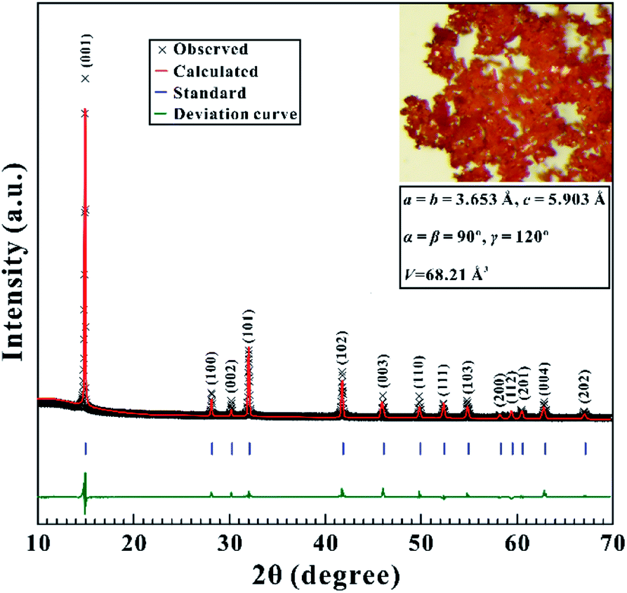
Available tin disulfide (SnS2) with high purity (99.99%) was commercially purchased from Hangzhou Kaiyada Company, Hangzhou, China. SnS2 powder samples were obtained by mechanically grinding bulk SnS2 in an agate mortar and were characterized by the X-ray diffraction (XRD) experiment. As displayed in Fig. 1, the Rietveld analysis result of the X-ray diffraction pattern can be well indexed into a hexagonal system (space group D3d3: P![[3 with combining macron]](https://www.rsc.org/images/entities/char_0033_0304.gif) m1) with the following lattice parameters: a = b = 3.653 Å, c = 5.903 Å, α = β = 90°, γ = 120°, and V = 68.21 Å3 at ambient conditions, which is in good agreement with the previous results of 2H-SnS2 (JCPDS No. 89-2358).1,14 These XRD results manifest the high quality of the SnS2 sample used in our experiments.
m1) with the following lattice parameters: a = b = 3.653 Å, c = 5.903 Å, α = β = 90°, γ = 120°, and V = 68.21 Å3 at ambient conditions, which is in good agreement with the previous results of 2H-SnS2 (JCPDS No. 89-2358).1,14 These XRD results manifest the high quality of the SnS2 sample used in our experiments.
 |
| | Fig. 1 The powder X-ray diffraction (XRD) pattern of SnS2 under ambient conditions and its corresponding structural refinement result. The red solid line and the black crosses stand for the calculated data and the observed data, respectively. The vertical bars denote the standard peak positions of SnS2. The green solid line represents the deviation curve. Inset: the optical microscope image of the starting SnS2 sample. | |
2.2 High-pressure Raman scattering measurements
High-pressure Raman scattering experiments of SnS2 have been performed in a piston-cylinder diamond anvil cell (DAC) with an anvil culet of 300 μm. High pressure was generated through turning four pressurization screws around the DAC equipment. First, a piece of clean T-301 stainless steel gasket (5 mm × 5 mm × 0.25 mm) was pre-indented to 50 μm thickness at approximately 10 GPa. Then, a 150 μm hole in the centre of the pre-indented area was drilled by a laser drilling machine as the experimental sample chamber. Subsequently, experimental samples and some tiny ruby single crystals were loaded into the sample chamber together. The pressure in the cell was calibrated according to the wavenumber shift of ruby fluorescence peaks.23 No pressure transmitting medium was employed to reach non-hydrostatic condition and helium was used as the pressure medium to provide hydrostatic condition. High-pressure Raman scattering experiments were conducted using a confocal Raman spectrometer (Invia, Renishaw 2000, England) equipped with an Olympus charge-coupled device camera. The Raman spectra of SnS2 were recorded under the operating conditions of excitation laser power of 50 mW and 0.5–40 μW with a 514.5 nm laser excitation source for Raman spectroscopy and fluorescence, respectively, and were collected within the wavenumber range from 150 cm−1 to 450 cm−1 with a resolution of 1.0 cm−1 in the backscattering geometry. Each Raman spectrum was gathered for 180 s. In order to prevent undulating pressure, a 15 minute interval between each Raman measurement was controlled at predesignated pressure points.
2.3 High-pressure electrical conductivity measurements
High-pressure electrical conductivity experiments of SnS2 were carried out utilizing a four column-type DAC with a couple of symmetrical 300 μm anvil culets taking advantage of its relatively larger lateral space, which has been extensively used in our previous electrical conductivity measurements.20,21,24 A mixture of cubic boron nitride (c-BN) powder and epoxy resin was compressed into a pre-indented T-301 gasket with 200 μm central hole. Subsequently, a new central hole with a diameter of 120 μm was drilled as the insulating sample chamber. Platinum electrodes with the thickness of 4 μm were separately integrated onto the upper and lower diamond anvils. No pressure transmitting medium was adopted to avoid introducing additional impurities, and as well as guarantee good contact between the sample and electrodes during electrical conductivity measurements. The alternating current (AC) impedance spectra of SnS2 were measured by a Solartron-1260 impedance/gain phase analyser (Schlumberger, Houston, TX, USA) within a frequency range of 10−1 to 107 Hz at predetermined signal voltages of 3000 mV and 50 mV for before and after the coupled structural–electronic transition of SnS2, respectively. For the high-pressure variable-temperature electrical conductivity measurements, low temperature was attained by the volatilization of liquid nitrogen. A k-type thermocouple with an error of ±5 K was attached to a side of a diamond to monitor the experimental temperature. Detailed statements on the high-pressure experimental methods and measurement procedures were reported in our other work.18,24,25
2.4 First-principles theoretical calculations
The first-principles theoretical calculations for SnS2 were implemented utilizing Kohn–Sham density functional theory (DFT) and pseudopotential methods in the Material Studio package with the standard Cambridge Sequential Total Energy Package (CASTEP) code.26 Electron exchange and correlation terms were described using the generalized gradient approximation (GGA) within the functional of Perdew–Burke–Ernzerhof (PBE) scheme.27 The Broyden–Fletcher–Goldfarb–Shanno (BFGS) minimization algorithm in CASTEP code was used for structural optimizations.28 Integration of the Brillouin zone was performed by using an 8 × 8 × 6 Monkhorst–Pack K-point grid for the relaxation and density of states (DOS). The kinetic cut off energy was set to 500 eV in order to keep high convergence.
3 Results and discussion
3.1 High-pressure Raman spectroscopy
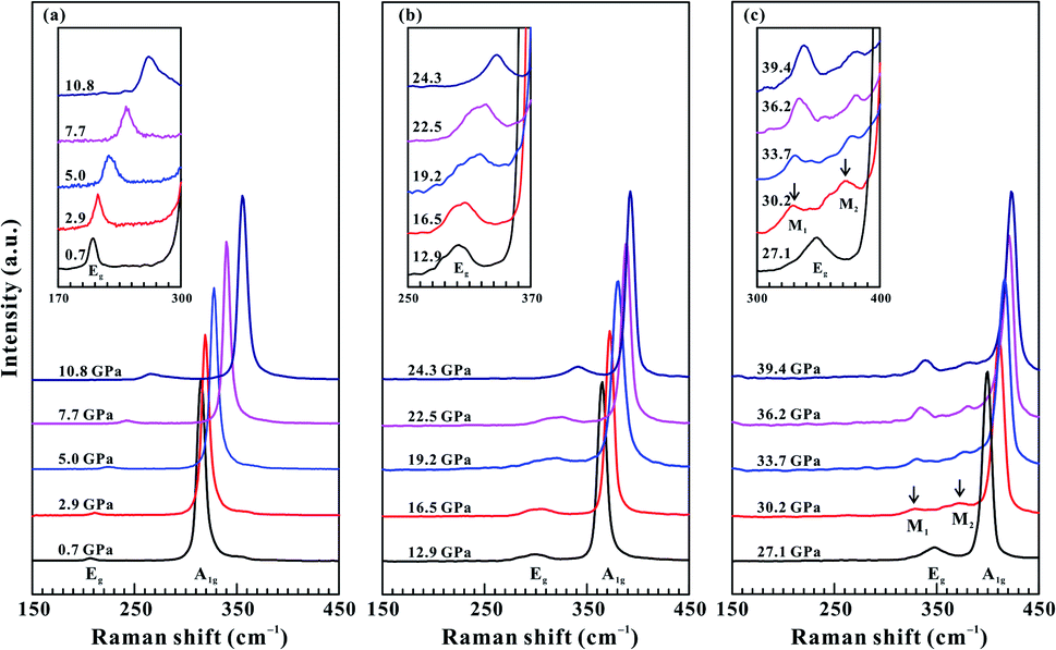
Raman spectroscopy has been considered as an effective and non-destructive method for exploring the electronic phase transition of layered metallic dichalcogenides.29–31 The in situ vibrational property of SnS2 has been investigated under non-hydrostatic condition up to 39.4 GPa and under hydrostatic condition up to 39.7 GPa. As shown in Fig. 2a, at the pressure of 0.7 GPa, a weak Raman-active peak at 206.7 cm−1 and another strong Raman-active peak at 314.7 cm−1 were detected within the wavenumber range of 150–450 cm−1 and they can be assigned as the in-plane Eg mode and out-of-plane A1g mode of 2H-SnS2, respectively. Our observed Raman peaks are in good consistent with previous Raman results at ambient conditions.16,17 To clearly illustrate the variations of the Eg, M1 and M2 modes with increasing pressure, we enlarged them in the insets of Fig. 2.
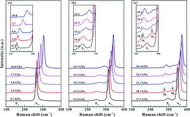 |
| | Fig. 2 Raman scattering spectra of SnS2 at different pressure points up to 39.4 GPa in the process of compression under non-hydrostatic condition. (a) 0.7–10.8 GPa; (b) 12.9–24.3 GPa; (c) 27.1–39.4 GPa. Inset: the corresponding enlarged figures of the Eg, M1 and M2 modes during compression. | |
Under non-hydrostatic condition, Fig. 2 and 3 present the Raman peaks, the Raman shifts, and the Raman full width at half maximum (FWHM) for SnS2 as a function of pressure up to 39.4 GPa. The observed Eg and A1g modes exhibited a monotonous shift toward higher wavenumbers as the pressure was increased and the pressure coefficient of the Eg mode was larger than that of the A1g mode, which manifests the pressure-induced anisotropy for SnS2. At 30.2 GPa, a splitting of the Eg mode into two modes was observed: a lower-frequency mode (denoted by M1) and a higher-frequency mode (denoted by M2) in Fig. 2c. Furthermore, through the analysis of the pressure-dependent Raman shifts and Raman FWHM for the Eg, A1g, M1 and M2 modes, one distinct discontinuity was also obtained at the pressure of 30.2 GPa. More specifically, the FWHM of the Eg mode had a positive slope in the pressure range of 0.7–27.1 GPa and yet negative slopes were observed for the M1 and M2 modes when the pressure was beyond 30.2 GPa (Fig. 3b). As for the A1g mode, its FWHM increased slowly with a rate of 0.03 cm−1 GPa−1 up to 30.2 GPa, while a large speed of 0.13 cm−1 GPa−1 was obtained in the pressure range of 30.2–39.4 GPa (Fig. 3c). The corresponding fitting results of the pressure-dependent Raman shifts and Raman FWHM under non-hydrostatic condition are listed in Table 1. In addition, the Raman peak intensity of SnS2 significantly decreased from 27.1 GPa to 30.2 GPa under non-hydrostatic condition (Fig. S3†). As usual, the variation in FWHM for A1g and Eg modes has close association with charge transfer processes, which has been widely applied to imply the occurrence of electronic phase transition for some layered metallic dichalcogenides.19,31 In the present study, the splitting of the Eg mode, the discontinuities in the pressure-dependent Raman shifts and FWHM for the Eg, A1g, M1 and M2 modes and the change of Raman intensity of SnS2 provide one clear clue for a pressure-induced coupled structural–electronic transition of SnS2 at 30.2 GPa. However, our Raman scattering results showed that there existed no apparent discontinuities in the pressure-dependent Raman shifts and Raman FWHM around 3.0 GPa, indicating that SnS2 remained stable in the lower pressure range. During decompression (Fig. S1†), the M1 and M2 Raman peaks started to vanish at 23.7 GPa under non-hydrostatic condition. Upon decompression down to ambient conditions, the recoverable Raman peak positions and shapes showed that the coupled structural–electronic transition is reversible during decompression. However, we found a considerable pressure hysteresis effect for the phase transition, which is probably related to the larger kinetic energy barrier in the process of decompression.
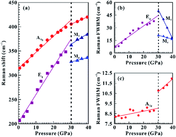 |
| | Fig. 3 (a) Pressure dependence of Raman shifts of the A1g, Eg, M1 and M2 modes for SnS2 under non-hydrostatic condition. (b and c) Pressure dependence of Raman FWHM of the A1g, Eg, M1 and M2 modes. The dashed and solid lines are used to guide to the eyes. | |
Table 1 Pressure dependence of Raman shifts and Raman FWHM for SnS2 in the process of compression under non-hydrostatic condition up to 39.4 GPa. ω is Raman shift, F is Raman FWHM and P is pressure
| |
Mode |
0.7–27.1 GPa |
30.2–39.4 GPa |
| Raman shifts (dω/dP) |
Eg |
5.68 |
— |
| A1g |
3.31 |
1.59 |
| M1 |
— |
1.13 |
| M2 |
— |
2.30 |
| Raman FWHM (dF/dP) |
Eg |
1.23 |
— |
| A1g |
0.03 |
0.13 |
| M1 |
— |
−0.49 |
| M2 |
— |
−3.50 |
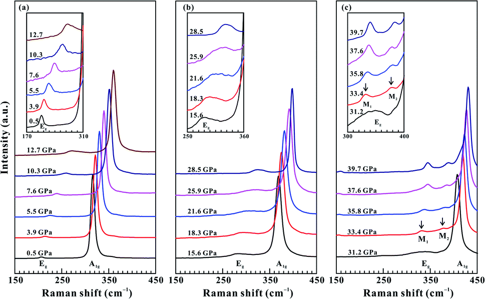
Under hydrostatic condition, the relationships of the Raman peaks, the Raman shifts and the Raman FWHM between pressure for SnS2 are displayed in Fig. 4 and 5. It makes clear that the variations in the pressure dependence of Raman peaks, Raman shifts and Raman FWHM were similar to those under non-hydrostatic condition. Table S1† shows the slope values of pressure-dependent Raman shifts and Raman FWHM under hydrostatic condition. However, a higher transition pressure of 33.4 GPa was obtained under hydrostatic condition than that under non-hydrostatic condition. Meanwhile, an obvious decrease in Raman intensity was also detected before and after the phase transition (see Fig. S4†). This discrepancy in the coupled structural–electronic transition of SnS2 under different hydrostatic environments can be attributed to the effect of the pressure medium. Under hydrostatic condition, helium was selected as the pressure transmitting medium, which can protect the crystalline structure of the sample from serious destruction induced by high pressure, and further delay the occurrence of the phase transition. However, under non-hydrostatic condition, no pressure transmitting medium was employed. Accordingly, the deviatoric stress inevitably formed and promoted the occurrence of the phase transition in layered SnS2. As a matter of fact, our previous studies have already revealed the influence of deviatoric stress on the pressure point of phase transition for other layered metallic chalcogenides (e.g., MoS2, MoSe2, ReS2, As2Te3).19–22 The Eg peak of SnS2 displayed an obvious broadening phenomenon at the pressure higher than 12.7 GPa, and resulting in a feeble peak splitting under hydrostatic condition. However, as for the non-hydrostatic condition, the Eg peak of sample was continuously variated up to the pressure of 27.1 GPa. Overall, the Raman full width at half maximum (FWHM) of the corresponding Eg mode for SnS2 showed a continuous increasing tendency with pressure below ∼30.0 GPa under different hydrostatic environments. In conclusion, all of these observed discontinuities in the Raman peak and its corresponding FWHM can provide a robust evidence for the occurrence of phase transition from a coupled structural–electronic transition in SnS2 at the pressure of ∼30.0 GPa under different hydrostatic environments. Upon decompression, a similar phase transition pressure was observed at 22.2 GPa under hydrostatic condition (Fig. S2†).
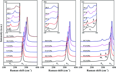 |
| | Fig. 4 Raman scattering spectra of SnS2 at different pressure points up to 39.7 GPa in the process of compression under hydrostatic condition. (a) 0.5–12.7 GPa; (b) 15.6–28.5 GPa; (c) 31.2–39.7 GPa. Inset: the corresponding enlarged figures of the Eg, M1 and M2 modes during compression. | |
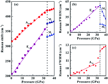 |
| | Fig. 5 (a) Pressure dependence of Raman shifts of the A1g, Eg, M1 and M2 modes for SnS2 under hydrostatic condition. (b and c) Pressure dependence of Raman FWHM of the A1g, Eg, M1 and M2 modes. The dashed and solid lines are used to guide to the eyes. | |
3.2 High-pressure electrical conductivity
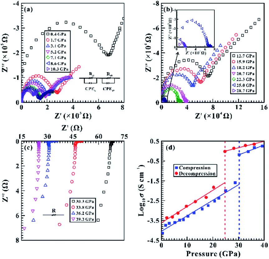
High-pressure and room-temperature electrical conductivity experiments were conducted to explore the electrical transport property of SnS2. Fig. 6a–c exhibit the measured impedance spectroscopy results of SnS2 at different pressure points up to 39.3 GPa. We employed ZView software to fit the impedance spectroscopy arcs obtained in the first quadrant and the oblique lines in the fourth quadrant. The fitting equivalent circuit consists of two parts in series and each part includes one resistance (R) and one constant phase element (CPE) in parallel for Fig. 6a and b, and consists of only one resistance (R) for Fig. 6c. The fitted error of the impedance spectra was controlled within 5%. In the pressure range of 0.4–28.7 GPa (Fig. 6a and b), semicircle arcs in the high frequency area (∼103 to 107 Hz) and oblique lines in the low frequency range (10−1 to 103) were observed in the impedance spectroscopy, which could be used to be representative of the grain interior resistance and the grain boundary resistance for SnS2, respectively. When the pressure was further increased from 30.3 to 39.3 GPa (Fig. 6c), all of the obtained grain interior resistances were observed in an oblique line way in the fourth quadrant.
 |
| | Fig. 6 Nyquist plots of SnS2 under ambient temperature and different pressure ranges of (a) 0.4–10.3 GPa; (b) 12.7–28.7 GPa; (c) 30.3–39.3 GPa. (d) Pressure dependence of logarithmic electrical conductivity of SnS2 in the both processes of compression and decompression. The dashed and solid lines serve as visual guides. | |
The electrical conductivity of SnS2 (σ) was calculated by the equation: σ = L/SR, where L stands for the experimental sample length (cm), S denotes the cross-section area of the electrode (cm2) and R is the resistance of the sample (Ω). In the present work, Fig. 6d exhibits the pressure dependence of the logarithmic electrical conductivity of SnS2 in the both processes of compression and decompression at room temperature. According to the discontinuities in the slope of pressure-dependent logarithmic electrical conductivity, two separate pressure ranges were distinguished: (i) within 0.4–28.7 GPa, the logarithmic electrical conductivities were negative values and enhanced quickly by nearly three orders of magnitude with a larger slope of 0.08 S cm−1 GPa−1; (ii) within 30.3–39.3 GPa, the electrical conductivities of 0.65–1.77 S cm−1 were comparable to the electrical conductivity values reported by previously available results on others layered metallic chalcogenides (e.g., MoS2, ReS2, Sb2S3, Ga2S3).21,22,25 Therefore, an apparent inflection point in the pressure-dependent electrical conductivity was acquired at 30.3 GPa, which suggests the occurrence of a coupled structural–electronic transition in SnS2. Furthermore, our observed phase transition pressure of SnS2 matches well with that obtained from Raman scattering at 30.2 GPa under non-hydrostatic condition. During decompression, the electrical conductivity value of the sample transformed back to its initial order of magnitude, indicating that the phase transition is reversible.
To further verify the coupled structural–electronic transition of SnS2 under compression, we performed variable-temperature electrical conductivity measurements under high pressure. Fig. 7a shows the in situ temperature-dependent electrical conductivities of SnS2 in the temperature range of 120–300 K at some representative pressure points of 20.1, 22.7, 25.6, 29.2, 31.5 and 34.7 GPa. In general, semiconductors are of a positive temperature–electrical conductivity relation, while a negative temperature–electrical conductivity relation can be observed for the coupled structural–electronic transition.31 To clearly discern the variation tendency of the electrical conductivities of SnS2 as a function of temperature before and after the phase transition, we magnified three trend lines at 29.2, 31.5 and 34.7 GPa in Fig. 7b–d, respectively. Below 31.5 GPa, the positive relationships between electrical conductivity and temperature showed the semiconducting behaviour of SnS2, whereas the negative relationships between electrical conductivity and temperature disclosed the metallic property of SnS2 when the pressure was beyond 31.5 GPa. Therefore, our temperature-dependent electrical conductivity experiments under high pressure confirmed the occurrence of the coupled structural–electronic transition in the process of compression. Actually, similar phase transition has been disclosed in other layered tin-bearing dichalcogenide of SnSe2.32 As for SnSe2, a lower metallization pressure of 15.2 GPa was obtained in comparison with SnS2, which is probably caused by the larger atom radius and electron orbitals of Se atom, leading to weaker interlayer electronic coupling in SnSe2. In addition, other layered metallic disulphides (e.g., MoS2, ReS2 and WS2)21,30,33 have been reported to undergo metallization under high pressure and thus it is maybe a common phenomenon among metallic disulphides.
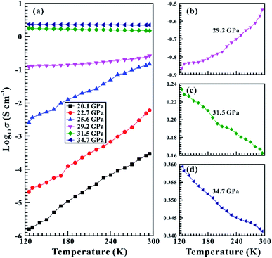 |
| | Fig. 7 Temperature-dependent logarithms of the electrical conductivity of SnS2 at certain representative pressure points. (a) Pressures are at 20.1, 22.7, 25.6, 29.2, 31.5 and 34.7 GPa. (b, c and d) The magnified curves at the points of 29.2, 31.5 and 34.7 GPa, respectively. | |
3.3 HRTEM of the starting and recovered samples
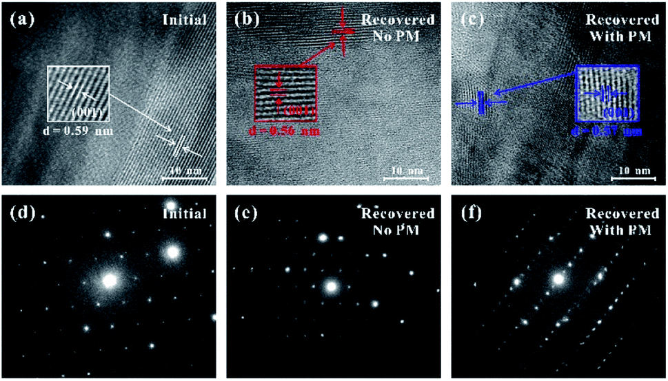
In order to further explore the reversibility of the pressure-induced coupled structural–electronic transition of SnS2 under different hydrostatic environments, some microstructural observations were conducted by means of high-resolution transmission electron microscopy (HRTEM). Fig. 8 exhibits the HRTEM images and corresponding cross-sectional selected-area electron diffraction (SAED) patterns. In here, Fig. 8a–c are the HRTEM images of the starting sample and the recovered samples decompressed from 38.4 and 39.1 GPa under non-hydrostatic and hydrostatic environments, respectively. Fig. 8d–f represent the corresponding cross-sectional SAED patterns. From Fig. 8a, typically crystalline stripes with an interplanar spacing of 0.59 nm were observed for the initial SnS2 sample, which is well consistent with the (001) oriented crystal plane of the layered SnS2. At the same time, its selected-area SAED pattern with electron diffraction spots (Fig. 8d) indicated a highly crystalline structure and an ordered arrangement. For the recovered SnS2 samples, the (001) interplanar spacings were measured to be 0.56 nm under non-hydrostatic condition (Fig. 8b) and 0.57 nm under hydrostatic condition (Fig. 8c). The slight decrease in the (001) interplanar spacing distance under different hydrostatic environments probably originates from the effect of the application of the pressure medium. Additionally, both the corresponding SAED patterns (Fig. 8e and f) took on some brightly diffraction spots and diffraction stripes, which reflected a high-degree crystalline structure in the recovered SnS2 samples. The HRTEM and SAED observations indicate a reversible change in the crystalline structure. Thus, these microscopic observations give a robust proof that the coupled structural–electronic transition of SnS2 was reversible under both non-hydrostatic and hydrostatic environments. This is in good agreement with the above-mentioned high-pressure Raman scattering results.
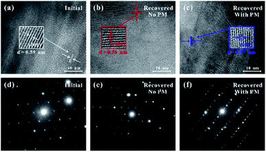 |
| | Fig. 8 HRTEM images and cross-sectional selected-area diffraction patterns of SnS2 samples. (a, b and c) HRTEM images of the starting sample and the recovered samples decompressed from 38.4 GPa and 39.1 GPa under non-hydrostatic and hydrostatic environments, respectively. (d–f) Cross-sectional selected-area electron diffraction patterns of the starting sample and the recovered samples. PM: pressure medium. | |
3.4 First-principles theoretical calculations of SnS2
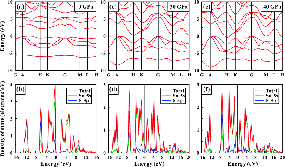
The first-principles theoretical calculations of SnS2 were performed on the basis of density functional theory to deeply understand the electronic behaviour of SnS2 under high pressure. Fig. 9 displays the calculated band gap energy and the total density and projected density of SnS2 at some representative pressure points of 0, 30 and 40 GPa. As shown in Fig. 9a, SnS2 belongs to a semiconductor with an indirect bandgap energy of 2.09 eV at atmospheric conditions, which is consistent with previously calculated results.1,14,34 And the corresponding total density and projected density are plotted in Fig. 9b, where the part of valence bands from −16 to 0 eV mainly came from the S-3p state. Beyond the Fermi-level (EF), the conduction bands were dominantly composed of the Sn-5s state. At the pressure of 30.0 GPa (Fig. 9c and d), the bandgap energy of SnS2 dropped to 0.04 eV and all energy bands was getting more broad than those at atmospheric pressure. When the pressure was further enhanced to 40.0 GPa (Fig. 9e and f), the conduction bands crossed the Fermi-level, showing that the metallic property of SnS2 formed. In short, the theoretical calculated results agreed well with our Raman and conductivity experimental data, supporting the pressure-induced coupled structural–electronic transition of SnS2.
 |
| | Fig. 9 (a, c and e) The calculated band structures of SnS2 at pressures of 0, 30 and 40 GPa, respectively. (b, d and f) The corresponding total density and projected density at 0, 30 and 40 GPa, respectively. The red dotted lines represent the position of the Fermi level. | |
4 Conclusions
In this paper, we reported a pressure-induced coupled structural–electronic transition of SnS2 using a diamond anvil cell in conjunction with in situ Raman scattering spectroscopy, AC impedance spectroscopy, high-resolution transmission electron microscopy and first-principles theoretical calculations. Upon compression, SnS2 underwent a pressure-induced coupled structural–electronic transition at 30.3 GPa under non-hydrostatic condition, while the phase transition was delayed by about 3.0 GPa under hydrostatic condition. Our first-principles theoretical calculations revealed that the coupled structural–electronic transition of SnS2 originates from the closure of band gap energy. Upon decompression, the phase transition was reversible under different hydrostatic environments, which was proved by our Raman, electrical conductivity and HRTEM observations.
Author contributions
Lidong Dai and Haiying Hu performed the conceptualization of this article and led the project. Xinyu Zhang and Meiling Hong performed the investigation including X-ray diffraction (XRD), high-pressure Raman spectra and high-pressure electrical conductivity measurements, high-resolution transmission electron microscopy analysis and first-principles theoretical calculations. Lidong Dai and Xinyu Zhang contributed to the analysis, interpretation and discussion of these results. Xinyu Zhang and Lidong Dai performed the writing-original draft. Lidong Dai, Haiying Hu, Xinyu Zhang, Meiling Hong and Chuang Li performed the writing-review & editing. All the authors commented on the final manuscript. Lidong Dai and Haiying Hu supervised the project.
Conflicts of interest
There are no conflicts to declare.
Acknowledgements
We thank the editor of Professor Jin-Ming Wu and two anonymous reviewers for their very constructive and enlightened comments and suggestions in the reviewing process, which helped us greatly improve the manuscript. Some kind guidance and help from Professor Heping Li in the Key Laboratory of High-temperature and High-pressure Study of the Earth's Interior, Institute of Geochemistry, Chinese Academy of Sciences are obtained for the in situ high-pressure Raman scattering measurements. This research was financially supported by the NSF of China (42072055, 41774099 and 41772042), Youth Innovation Promotion Association of CAS (Grant No. 2019390), and as well as Special Fund of the West Light Foundation of CAS.
References
- L. A. Burton, T. J. Whittles, D. Hesp, W. M. Linhart, J. M. Skelton, B. Hou, R. F. Webster, G. O'Dowd, C. Reece, D. Cherns, D. J. Fermin, T. D. Veal, V. R. Dhanak and A. Walsh, J. Mater. Chem. A, 2016, 4, 1312–1318 RSC.
- W. Chu, X. Li, S. Li, J. Hou, Q. Jiang and J. Yang, ACS Appl. Energy Mater., 2018, 2, 382–388 CrossRef.
- L. Gao, C. Chen, K. Zeng, C. Ge, D. Yang, H. Song and J. Tang, Light: Sci. Appl., 2016, 5, e16126 CrossRef CAS PubMed.
- B. Giri, M. Masroor, T. Yan, K. Kushnir, A. D. Carl, C. Doiron, H. Zhang, Y. Zhao, A. McClelland, G. A. Tompsett, D. Wang, R. L. Grimm, L. V. Titova and P. M. Rao, Adv. Energy Mater., 2019, 9, 1901236 CrossRef.
- R. K. Gupta and F. Yakuphanoglu, Sol. Energy, 2012, 86, 1539–1545 CrossRef CAS.
- Y. Huang, E. Sutter, J. T. Sadowski, M. Cotlet, O. L. A. Monti, D. A. Racke, M. R. Neupane, D. Wickramaratne, R. K. Lake, B. A. Parkinson and S. Peter, ACS Nano, 2014, 8, 10743–10755 CrossRef CAS PubMed.
- M. Liu, J. Yang, Q. Qu, P. Zhu and W. Li, J. Power Sources, 2015, 273, 848–856 CrossRef CAS.
- G. Liu, Y. Qiu, Z. Wang, J. Zhang, X. Chen, M. Dai, D. Jia, Y. Zhou, Z. Li and P. Hu, ACS Appl. Mater. Interfaces, 2017, 9, 37750–37759 CrossRef CAS PubMed.
- J. Z. Ou, W. Ge, B. Carey, T. Daeneke, A. Rotbart, W. Shan, Y. Wang, Z. Fu, A. F. Chrimes, W. Wlodarski, S. P. Russo, Y. X. Li and K. Kalantar-zadeh, ACS Nano, 2015, 9, 10313–10323 CrossRef CAS PubMed.
- H. S. Song, S. L. Li, L. Gao, Y. Xu, K. Ueno, J. Tang, Y. B. Cheng and K. Tsukagoshi, Nanoscale, 2013, 5, 9666–9670 RSC.
- J. Yu, C. Y. Xu, F. X. Ma, S. P. Hu, Y. W. Zhang and L. Zhen, ACS Appl. Mater. Interfaces, 2014, 6, 22370–22377 CrossRef CAS PubMed.
- B. Palosz, W. Steurer and H. Schulz, Acta Crystallogr., Sect. B: Struct. Sci., 1990, 46, 449–455 CrossRef.
- G. Domingo, R. S. Itoga and C. R. Kannewurf, Phys. Rev., 1966, 143, 536–541 CrossRef CAS.
- M. O. Filsø, E. Eikeland, J. Zhang, S. R. Madsen and B. B. Iversen, Dalton Trans., 2016, 45, 3798–3805 RSC.
- K. Knorr, L. Ehm, M. Hytha, B. Winkler and W. Depmeier, Phys. Status Solidi B, 2001, 223, 435–440 CrossRef CAS.
- S. V. Bhatt, M. P. Deshpande, V. Sathe and S. H. Chaki, Solid State Commun., 2015, 201, 54–58 CrossRef CAS.
- A. N. Utyuzh, Y. A. Timofeev and G. N. Stepanov, Phys. Solid State, 2010, 52, 352–356 CrossRef CAS.
- L. Dai, Y. Zhuang, H. Li, L. Wu, H. Hu, K. Liu, L. Yang and C. Pu, J. Mater. Chem. C, 2017, 5, 12157–12162 RSC.
- L. Yang, L. Dai, H. Li, H. Hu, K. Liu, C. Pu, M. Hong and P. Liu, RSC Adv., 2019, 9, 5794–5803 RSC.
- L. Yang, J. Jiang, L. Dai, H. Hu, M. Hong, X. Zhang, H. Li and P. Liu, J. Mater. Chem. C, 2021, 9, 2912–2918 RSC.
- Y. Zhuang, L. Dai, L. Wu, H. Li, H. Hu, K. Liu, L. Yang and C. Pu, Appl. Phys. Lett., 2017, 110, 122103 CrossRef.
- Y. Zhuang, L. Dai, H. Li, H. Hu, K. Liu, L. Yang, C. Pu, M. Hong and P. Liu, J. Phys. D: Appl. Phys., 2018, 51, 165101 CrossRef.
- H. K. Mao, J. Xu and P. M. Bell, J. Geophys. Res., 1986, 91, 4673 CrossRef CAS.
- L. Dai, C. Pu, H. Li, H. Hu, K. Liu, L. Yang and M. Hong, Rev. Sci. Instrum., 2019, 90, 066103 CrossRef PubMed.
- L. Dai, K. Liu, H. Li, L. Wu, H. Hu, Y. Zhuang, L. Yang, C. Pu and P. Liu, Phys. Rev. B, 2018, 97, 024103 CrossRef.
- S. J. Clark, M. D. Segall, C. J. Pickard, P. J. Hasnip, M. I. J. Probert, K. Refson and M. C. Payne, Z. Kristallogr.–Cryst. Mater., 2005, 220, 567–570 CrossRef CAS.
- J. P. Perdew, K. Burke and M. Ernzerhof, Phys. Rev. Lett., 1996, 77, 3865–3868 CrossRef CAS PubMed.
- T. H. Fischer and J. Almlof, J. Phys. Chem., 1992, 96, 9768–9774 CrossRef CAS.
- Z. H. Chi, X. M. Zhao, H. Zhang, A. F. Goncharov, S. S. Lobanov, T. Kagayama, M. Sakata and X. J. Chen, Phys. Rev. Lett., 2014, 113, 036802 CrossRef CAS PubMed.
- S. Duwal and C.-S. Yoo, J. Phys. Chem. C, 2016, 120, 5101–5107 CrossRef CAS.
- A. P. Nayak, S. Bhattacharyya, J. Zhu, J. Liu, X. Wu, T. Pandey, C. Jin, A. K. Singh, D. Akinwande and J. F. Lin, Nat. Commun., 2014, 5, 3731 CrossRef CAS PubMed.
- Y. Zhou, B. Zhang, X. Chen, C. Gu, C. An, Y. Zhou, K. Cai, Y. Yuan, C. Chen, H. Wu, R. Zhang, C. Park, Y. Xiong, X. Zhang, K. Wang and Z. Yang, Adv. Electron. Mater., 2018, 4, 1800155 CrossRef.
- D. Zhou, Y. Zhou, C. Pu, X. Chen, P. Lu, X. Wang, C. An, Y. Zhou, F. Miao, C.-H. Ho, J. Sun, Z. Yang and D. Xing, npj Quantum Mater., 2017, 2, 19 CrossRef.
- J. M. Gonzalez and I. I. Oleynik, Phys. Rev. B, 2016, 94, 125443 CrossRef.
Footnote |
| † Electronic supplementary information (ESI) available. See DOI: 10.1039/d1ra08632d |
|
| This journal is © The Royal Society of Chemistry 2022 |
Click here to see how this site uses Cookies. View our privacy policy here. 
 Open Access Article
 This Open Access Article is licensed under a Creative Commons Attribution-Non Commercial 3.0 Unported Licence
 *a,
Haiying Hu
*a,
Haiying Hu