DOI:
10.1039/D1RA08022A
(Paper)
RSC Adv., 2022,
12, 3191-3197
Synthesis and characterization of naphthalene derivatives for two-component heterojunction-based ambipolar field-effect transistors complemented with copper hexadecafluorophthalocyanine (F16CuPc)
Received
1st November 2021
, Accepted 28th December 2021
First published on 25th January 2022
Abstract
In order to develop organic semiconductor materials with good performance, herein, a series of naphthalene derivatives were designed and synthesized by a “building-blocks approach” connected through α-bond, double bond, and triple bond, respectively. Thin-film transistors were fabricated in single-component and two-component modes based on these naphthalene derivatives by combining the F16CuPc as the n-type material. The ambipolar performance was investigated by adjusting the device preparation procedure with the hole and electron mobility of up to 10−2 cm2 V−1 s−1. Furthermore, the electrical performance was also improved to 0.73 cm2 V−1 s−1 using the two-component bilayer configuration.
Introduction
Over the past decades, organic field effect transistors (OFETs) have attracted extensive attention and development due to their high mobility speeds, low cost, light weight, large-area preparation and good compatibility with flexible substrates.1–5 In particular, for constructing complementary circuits, ambipolar OFETs have become highly desired due to their advantage of simultaneously providing both n- and p-channel performance in a single device.6–11 According to the composition of the semiconducting layer, ambipolar OFET devices can be fabricated by the single-component, two-component bilayer and two-component blending thin-film modes. For the single-component mode, in which the highest occupied molecular orbital (HOMO) and lowest unoccupied molecular orbital (LUMO) energy levels of the semiconductor materials need to be simultaneously matched with the same metal electrode, it is difficult to simultaneously achieve a balanced and high hole and electron mobility because of the problem of unequal charge carrier injection into the semiconductor. Since Dodabalapur and coworkers reported the first ambipolar OFET device by means of a bilayer technique based on p-type α-hexathienylene and n-type C60 semiconductors,12 the two-component bilayer mode has become an important alternative and attracted significant research interest, although it is even more difficult to understand its working mechanism than the single-component mode. A series of two-component bilayer OFETs were investigated by combining p-type and n-type organic semiconductors, including small molecules and even polymers such as phenacene/perylene,13 pentacene/PTCDI-C13H27,14 pentacene/C60,15 BP2T/F16CuPc16 and CuPc/F16CuPc,17 etc. In particular, fluorinated metal phthalocyanines, such as hexadecafluorophthalocyanine (F16CuPc), have demonstrated potential advantages in constructing ambipolar OFETs as typical n-type organic semiconductors due to their excellent electrical and optical properties as well as air-stable properties.16–19
Naphthalene is widely used in the synthesis of organic photo-electronic materials as a building block due to its stable structure, cheap price and easy halogenations at the 2- and 6- positions.20–26 Its bromides, such as 2-bromonaphthalene and 2,6-dibromonaphthalene, are easily and commercially available, which is conducive to future industrialization. The “building-blocks approach” is one important way to develop organic semiconductor materials.27 By the combination of various building blocks, new molecules can be produced conveniently. Moreover, the mode of connection, which includes α-, double and triple bonds, etc., could significantly affect the material properties.28–33
In order to develop organic semiconductor materials with good performance, herein, a series of naphthalene derivatives were designed and synthesized by the “building-blocks approach,” connected through the α-bond, double bond and triple bond, respectively. Thin-film transistor devices were fabricated based on these compounds, and the highest mobility of up to 0.53 cm2 V−1 s−1 was achieved for the single-component devices. Furthermore, two-component bilayer OFETs devices were prepared by combining the naphthalene derivatives with F16CuPc as the n-type material. The ambipolar performance was investigated by adjusting the bilayer configuration, and the electrical performance was also improved by the device preparation procedure.
Results and discussion
Synthesis
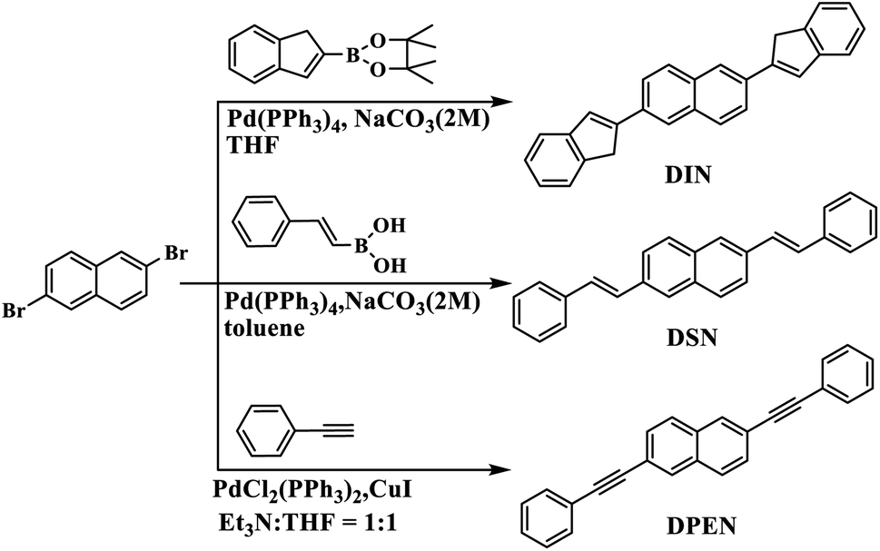
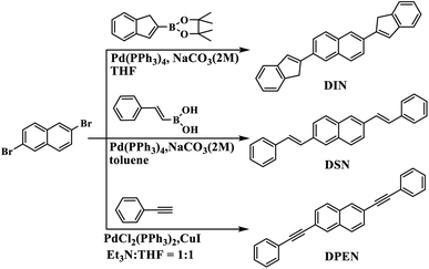
The synthetic routes of naphthalene derivatives 2,6-di(1H-inden-2-yl) naphtha-ene (DIN), 2,6-di((E)-styry)naphthalene (DSN) and 2,6-bis(phenylthyny)naphtha-ene (DPEN) are described in Scheme 1. Compounds DSN and DIN were synthesized directly through Suzuki coupling reaction between 2,6-dibromonaphthalene and boric acid intermediate. Compound DPEN was synthesized through a Sonogashira coupling reaction between 2,6-dibromonaphthalene and ethynylbenzene. Purification was carried out by column chromatography, followed by recrystallization, and the chemical structure was thoroughly characterized by mass spectrometry, 1H-NMR and elemental analysis.
 |
| | Scheme 1 Synthetic routes for naphthalene derivatives. | |
Thermal, optical and electrochemical properties
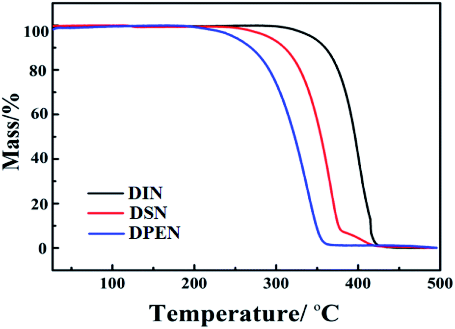
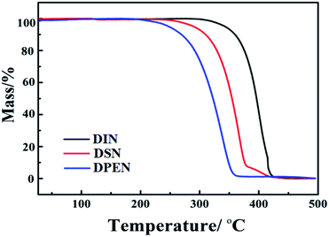
The thermal properties of the naphthalene derivatives were measured by thermogravimetric analysis (TGA) under nitrogen atmosphere, as shown in Fig. 1 and Table 1. When the weight loss was about 5%, the thermal decomposition temperatures of DIN, DSN and DPEN were 350 °C, 300 °C and 250 °C, respectively, indicating that all the derivatives showed good thermal stability, and that the introduction of unsaturated bonds reduced the thermal stability of the compounds.
 |
| | Fig. 1 TGA results of the naphthalene derivatives. | |
Table 1 Thermal, photophysical, and electrochemical properties and the calculated energy levels of the naphthalene derivativesa
| Compds |
DIN |
DSN |
DPEN |
| Eg,opa was determined from the onset of the UV-vis absorption spectra in solution. HOMOa = −4.8 + EFc − Eox,1/2; LUMOa = HOMO + Eg,op. HOMOb and LUMOb are based on the DFT (B3LYP/6-31G(d)) calculations. |
| Td/°C |
350 |
300 |
250 |
| λonset,ox/nm |
393 |
401 |
367 |
| Eg,opa/eV |
3.16 |
3.09 |
3.38 |
| Eox,1/2 |
1.13 |
1.26 |
1.58 |
| HOMOa/eV |
−5.53 |
−5.66 |
−5.98 |
| LUMOa/eV |
−2.37 |
−2.57 |
−2.60 |
| HOMOb/eV |
−5.02 |
−5.12 |
−5.36 |
| LUMOb/eV |
−1.76 |
−1.88 |
−1.82 |
| Egb/eV |
3.26 |
3.24 |
3.54 |
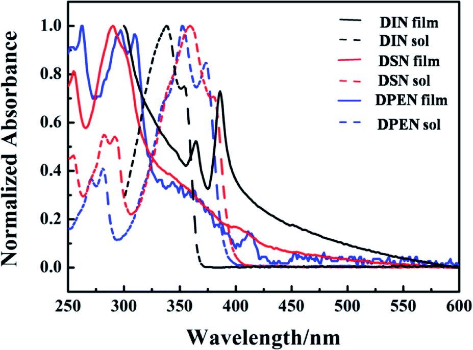
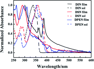
The optical properties of the naphthalene derivatives were investigated by UV-vis absorption spectroscopy. As shown in Fig. 2 and Table 1, the maximum absorption peak of the compounds DIN, DSN and DPEN in CH2Cl2 solution are located at 339 nm, 359 nm and 354 nm, respectively, which correspond to the π–π transition band of the three compounds. According to the initial absorption wavelengths, the band gaps are 3.16 eV, 3.09 eV and 3.38 eV, respectively, which were calculated using the equation Eg = 1240/λonset. Compared with that in solution, the spectral absorption of DIN vacuum-deposited thin film on a quartz substrate was red-shifted, and the thin films of DPEN and DSN were blue-shifted.
 |
| | Fig. 2 Normalized UV-vis absorption spectra of the naphthalene derivatives in CH2Cl2 solution and as thin films. | |
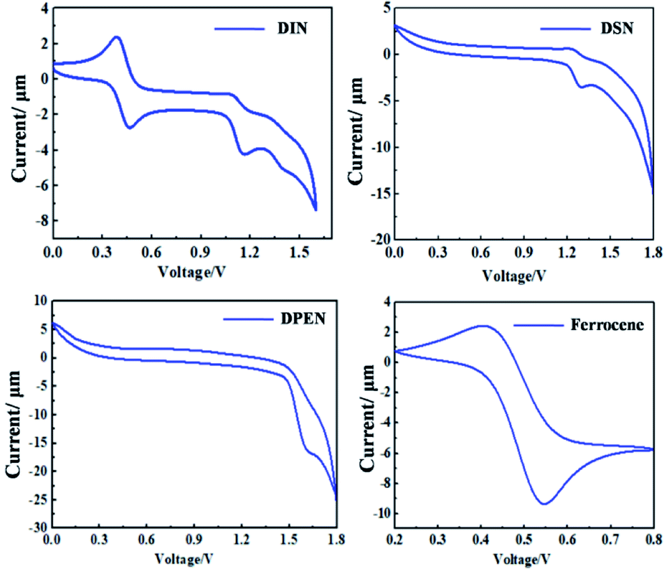
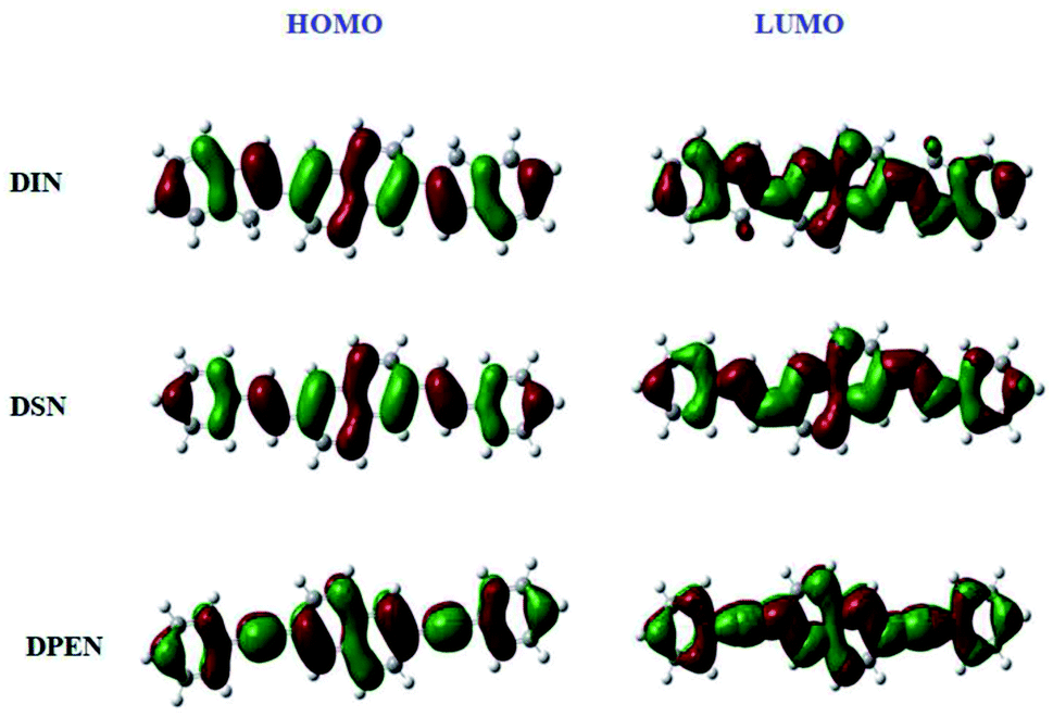
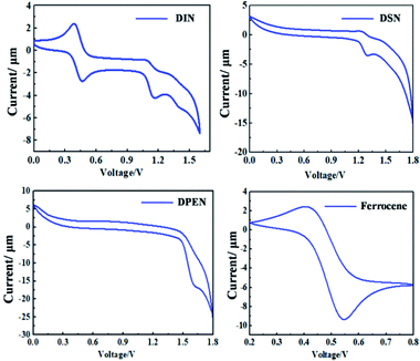
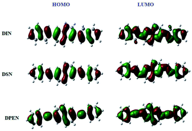
The redox properties of the naphthalene derivatives were measured in CH2Cl2 solution by cyclic voltammetry (CV). As shown in Fig. 3 and Table 1, the HOMO levels of DIN, DSN and DPEN are −5.53 eV, −5.66 eV and −5.98 eV, respectively, which were calculated by the formula EHOMO = −4.8 + EFc − Eox using ferrocene as internal standard.34,35 Then, by combining with their optical band gaps, the LUMO energy levels were calculated to be −2.37 eV, −2.57 eV and −2.60 eV, respectively. Furthermore, the molecular-orbital calculations of the HOMO and LUMO levels were performed using the density functional theory (DFT) method (B3LYP,6-13G(d)) to confirm the redox properties of the naphthalene derivatives (see Fig. 4). The simulated results also imply the good oxidation stability of DIN, DSN and DPEN.
 |
| | Fig. 3 Cyclic voltammograms of the naphthalene derivatives. | |
 |
| | Fig. 4 HOMO and LUMO orbitals of the naphthalene derivatives obtained using DFT calculations. | |
Thin film crystallinity and morphology
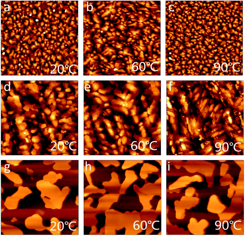
The morphology and crystallinity of thin films are closely related to the charge transfer performance. Thin films of the naphthalene derivatives were deposited onto a octadecyl-trichlorosilane (OTS) modified silicon wafer by vacuum evaporation and were characterized using atomic force microscopy (AFM) and X-ray diffraction (XRD). As shown in Fig. 5, at room temperature (Tsub = 20 °C), the crystal grain of DIN is granulous and DSN is clustered; both grain sizes are small. DPEN forms a sheet-like shape, and the size even reaches 2 μm, but the grain boundary is also obviously large. With an increase in the substrate temperature to 60 °C, all the grain sizes become larger, and the grain boundary becomes smaller, indicating that the semiconductor layers present better consecutiveness and less traps, which are conducive to the transport of carriers; thus the electrical performance of the device could be improved. When the substrate temperature was raised to 90 °C, the grain size of DIN was significantly reduced, DSN was destroyed, and the grain boundary of DPEN was enlarged, which is usually unfavorable for OFET performance.
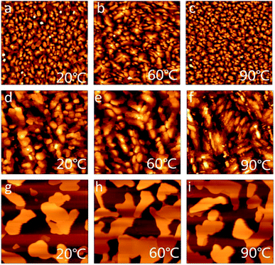 |
| | Fig. 5 AFM images (5 μm × 5 μm) of the thin films of DIN (a–c), DSN (d–f) and DPEN (g–i) deposited at different temperatures. | |
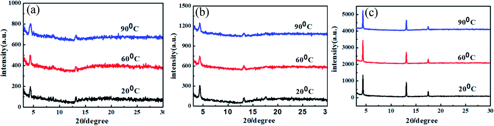
XRD measurements of the thin films deposited at different temperatures showed similar primary diffraction peaks at 2θ = 4.46°, 4.35° and 4.34° for DIN, DSN and DPEN, respectively (see Fig. 6). The primary peaks showed distinct diffraction, and the corresponding d-spacings were 1.949 nm, 2.028 nm and 2.037 nm, respectively. The values of the d-spacings are very close to the length of the molecules, which indicates that the molecules are oriented almost perpendicularly to the substrate and that the π–π stacking direction is parallel to the substrate.
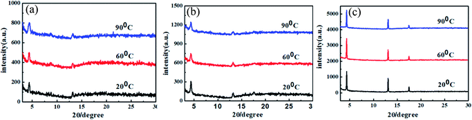 |
| | Fig. 6 X-ray diffraction of the thin films of (a) DIN, (b) DSN and (c) DPEN deposited at different temperatures. | |
OFET performance
Thin-film transistors of DIN, DSN and DPEN were fabricated in top-contact configuration using gold as source and drain electrodes, and doped silicon as the gate electrode. All the devices showed typical p-channel FET properties under ambient conditions. DSN exhibits excellent OFET performance, which is higher by one to two orders of magnitude than that of the other two materials. With increasing substrate temperature, the performance of DIN, DSN and DPEN improved. When the substrate temperature was increased to 60 °C, the device performance was highest, and the mobility of DIN, DSN and DPEN reached up to 5.40 × 10⁻² cm2 V−1 s−1, 0.53 cm2 V−1 s−1 and 3.42 × 10⁻² cm2 V−1 s−1, respectively. Fig. 7 shows the transfer and output curves of DIN, DSN and DPEN at Tsub = 60 °C, and the OFET performance obtained at different substrate temperatures is summarized in Table 2. With further increasing the substrate temperature (Tsub = 90 °C), the mobility decreased dramatically, which could be caused by the worse morphologies of the films evidenced by AFM.
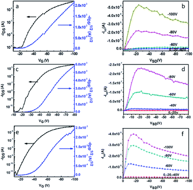 |
| | Fig. 7 Typical transfer (left) and out (right) curve of DIN (a and b), DSN (c and d) and DPEN (e and f). | |
Table 2 OFET characteristics of the naphthalene derivatives deposited at different annealing temperatures
| Compds |
Tsub °C |
μ (cm2 V−1 s−1) |
Vt [V] |
On/off ratio |
| DIN |
rt |
4.80 × 10⁻³ |
−42 |
6 × 10³ |
| 60 |
5.40 × 10⁻² |
−38 |
1 × 10⁶ |
| 90 |
6.25 × 10⁻³ |
−45 |
1 × 10⁴ |
| DSN |
rt |
0.17 |
−29 |
4 × 10⁴ |
| 60 |
0.53 |
−35 |
8 × 10⁶ |
| 90 |
0.21 |
−47 |
1 × 10⁴ |
| DPEN |
rt |
6.80 × 10⁻³ |
−42 |
3 × 10³ |
| 60 |
3.42 × 10⁻² |
−36 |
1 × 10⁴ |
| 90 |
8.1 × 10⁻⁴ |
−38 |
1 × 10³ |
To obtain ambipolar OFET performance, DSN was used as the p-type active semiconductor material and F16CuPc as the n-type semiconductor to construct bilayer heterojunction devices. Both materials were put into a vacuum chamber and deposited onto OTS-modified silicon wafer successively. The substrate temperature was kept at 60 °C and without oxygen contact during the evaporation switching. The preparation procedure of the gold electrode was the same as the above unipolar devices. The F16CuPc was deposited firstly onto the silicon wafer at different thicknesses, and DSN was then deposited up to 15 nm.
When the thickness of F16CuPc is 2 nm or 6 nm, the transistors exhibit obvious ambipolar properties, with hole and electronic mobilities of up to 10−2 cm2 V−1 s−1 (see Fig. 8 and Table 3). With the increasing thickness of F16CuPc, the electronic mobility increased, but the hole transport characteristics disappeared. For contrast, the DSN was deposited firstly, and F16CuPc was then deposited up to 10 nm. When the thickness of DSN is 2 nm or 6 nm, the transistors only exhibit p-type properties. With the thickness of DSN increased to 10 nm, the transistors exhibit obvious ambipolar properties, with hole and electronic mobilities of up to 0.46 cm2 V−1 s−1 and 2.5 × 10⁻³ cm2 V−1 s−1, respectively. It is worth noting that the hole mobility increased to 0.73 cm2 V−1 s−1 when the thickness of F16CuPc was reduced to 5 nm, and the electronic mobility lowered by one order of magnitude. In this case, F16CuPc could mainly act as a dopant, not only as n-type acceptor material. Furthermore, DSN and F16CuPc were blended and co-evaporated onto an OTS-modified silicon wafer, and the obtained transistors only display p-channel FET properties with mobility up to 7.4 × 10⁻² cm2 V−1 s−1, and the electronic transport characteristics could not be detected. These results demonstrate that the ambipolar electrical performance could be effectively regulated by the device configuration and film thickness.
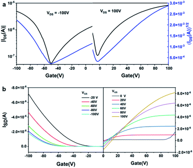 |
| | Fig. 8 Typical transfer (a) and out (b) curves of the ambipolar OFETs based on the DSN/F16CuPc bilayer heterojunction devices. | |
Table 3 OFET characteristics of two-component bilayer heterojunction-based transistors with different configurations and thicknesses of DSN/F16CuPc thin films
| DSN/F16CuPc |
μe |
μh |
F16CuPc/DSN |
μe |
μh |
| The unit of thickness of the semiconductor layer is nm. The unit of mobility is cm2 V−1 s−1. |
| 15/2 |
7.5 × 10⁻³ |
0.01 |
10/2 |
No |
0.042 |
| 15/6 |
0.023 |
0.065 |
10/6 |
No |
0.063 |
| 15/10 |
0.031 |
No |
10/10 |
2.5 × 10⁻³ |
0.46 |
| 15/15 |
0.048 |
No |
5/10 |
2.2 × 10⁻⁴ |
0.73 |
Experimental
General
All reagents and chemicals were purchased from J&K Scientific and Aladdin and were used without further purification. 1H-NMR spectra were recorded on a Bruker DRX-400 Spectrometer with Si(CH3)4 as an external standard. Mass spectrometry (MS) was performed on a MicroTOF-Q II. Elemental analyses were performed by the CRMPO. The UV-vis spectrum was obtained on a TU-1901 double-beam UV-vis spectrophotometer. Thermogravimetric analysis (TGA) was carried out on a TAQ500. Cyclic voltammetry (CV) was performed on a CHI660C electrochemistry station in a dichloromethane solution using 0.1 M tetrabutylammonium hexafluorophosphate (Bu4NPF6) as supporting electrolyte at a scan rate of 100 mV s−1, using glass carbon as working electrode, Pt wire as counter electrode and Ag/AgCl as reference electrode. AFM images of the film morphology were obtained using an atomic force microscope in tapping mode. XRD measurements were carried out in reflection mode using a PAN analytical X'pert powder diffraction system. The electrical characteristics of the devices were examined using a Keithley 4200 semiconductor parameter analyzer at room temperature in air.
Thin-film transistor device fabrication
OFET devices were fabricated by the bottom-gate/top-contact geometry configuration. A 50 nm thick organic semiconductor film was deposited onto the OTS-modified SiO2 substrate by vacuum evaporation at different substrate temperatures. Gold electrodes were deposited using a copper shadow mask with the channel length and width of 31 and 273 μm, respectively. The field effect properties were measured under ambient conditions. For the two-component bilayer devices, the thickness of semiconductor materials is listed in Table 3, and the thickness of the gold electrode is 20 nm.
Synthesis
2,6-di(1H-inden-2-yl)naphthalene (DIN). 2,6-Dibromonaphthalene (572 mg, 2 mmol) was added to a 250 ml round-bottom flask. After it was degassed and purged with nitrogen, 80 ml of dry tetrahydrofuran solution was added, then 1H-indole-2-boronic acid pinacol ester (1000 mg, 4.13 mmol) and Pd(PPh3)4 (231 mg, 0.2 mmol) were quickly added. After again purging with nitrogen, a solution of Na2CO3 (2 M, 40 ml) was added, and the mixture was heated to reflux for 48 h. After the reaction was completed, the mixture was cooled to room temperature and filtered, and the precipitate was collected and washed with water and methanol, sequentially. After purification by silica gel column chromatography, the title product was recrystallized from chloroform to give 330 mg of pure compound DIN (yield 46%). MS (MALDI-TOF): 356.0. 1H NMR (400 MHz, CDCl3): δ 7.97 (m, 2H), 7.84 (m, 4H), 7.52 (m, 4H), 7.37 (m, 4H), 7.00 (s, 2H), 3.94 (s, 4H). Anal. calcd for C28H20: C, 94.34; H, 5.66. Found: C, 92.92; H, 5.53.
2,6-di((E)-styryl)naphthalene (DSN). 2,6-dibromonaphthalene (572 mg, 2 mmol) was added to a 250 ml round-bottom flask and evacuated by vacuum, then 60 ml of dry toluene solution was added. Under nitrogen condition, trans-BETA-styrene boronic acid (600 mg, 4 mmol) and Pd(PPh3)4 (231 mg, 0.2 mmol) were quickly added and purged with nitrogen. After Na2CO3 aqueous solution (2 M, 25 ml) was added, the mixture was heated and refluxed for 48 h. After completion of the reaction, the mixture was cooled to room temperature. The crude product was purified by silica gel column chromatography and recrystallized from chloroform to give 276 mg of pure compound DSN (yield 42%). MS (MALDI-TOF): 332.0. 1H NMR (400 MHz, CDCl3): δ 7.82 (s, 2H), 7.74 (d, 2H), 7.57 (d, 2H), 7.52 (m, 4H), 7.39 (m, 4H), 7.30 (m, 2H), 7.08 (d, 4H). Anal. Calcd for C26H20: C, 93.94; H, 6.06. Found: C, 89.96; H, 5.88.
2,6-Di(phenylethynyl)naphthalene (DPEN). 2,6-Dibromonaphthalene (572 mg, 2 mmol), PdCl2 (PPh3)2 (90 mg, 0.128 mmol) and CuI (24 mg, 0.126 mmol) were added to a round flask. A solution of 20 ml of triethylamine and 20 ml of anhydrous tetrahydrofuran was added. Then, phenylacetylene (102 mg, 4 mmol) was quickly added under nitrogen atmosphere, and the mixture was heated to reflux for 30 h. After the reaction was completed, the mixture was cooled to room temperature, and the crude product was concentrated. The residue was purified by silica gel column chromatography and recrystallized from chlorobenzene to give 300 mg of DPEN (yield 45%). MS (MALDI-TOF): 329.13. 1H NMR (400 MHz, CDCl3): δ 8.03 (s, 2H), 7.79 (d, 2H), 7.61–7.57 (m, 6H), 7.41–7.36 (m, 6H). Anal. calcd for C26H16: C, 95.09; H, 4.91. Found: C, 91.82; H, 4.83.
Conclusions
In summary, a series of novel naphthalene derivatives (DIN, DSN and DPEN) were synthesized. These compounds show high stability, which was confirmed by TGA, UV-vis spectra and cyclic voltammetry. The morphology and crystallinity of the semiconductor thin films were characterized by AFM and XRD, respectively. A high mobility of up to 0.53 cm2 V−1 s−1 was achieved for the thin film transistor of DSN, which is higher by one to two orders of magnitude than that of the DIN and DPEN. Furthermore, two-component bilayer OFET devices were prepared by combining DSN with F16CuPc as the p-type and n-type material, respectively. Ambipolar performance was obtained by adjusting the device preparation procedure, with hole and electronic mobilities of up to 10−2 cm2 V−1 s−1. Furthermore, the electrical performance was increased to 0.73 cm2 V−1 s−1 using a two-component bilayer configuration. These results suggest that the two-component bilayer configuration not only can achieve ambipolar OFETs but also could contribute to enhancing the electrical performance compared to single-component devices.
Conflicts of interest
There are no conflicts to declare.
Acknowledgements
The authors acknowledge financial support from the National Natural Science Foundation of China (21272049), the Ministry of Science and Technology of China (2013CB933500), and the Project for the Innovation of High Level Returned Overseas Scholars (or team) in Hangzhou, Beijing Science and Technology Project (code Z201100008420019).
Notes and references
- H. Yan, Z. Chen, Y. Zheng, C. Newman, J. R. Quinn, F. Dotz, M. Kastler and A. Facchetti, Nature, 2009, 457, 679–686 CrossRef CAS PubMed.
- W. Hu, Organic Optoelectronics, Wiley–VCH, 2013 Search PubMed.
- W. Wu, Y. Liu and D. Zhu, Chem. Soc. Rev., 2010, 39, 1489–1502 RSC.
- C. Wang, H. Dong, W. Hu, Y. Liu and D. Zhu, Chem. Rev., 2012, 112, 2208–2267 CrossRef CAS PubMed.
- H. Dong, C. Wang and W. Hu, Chem. Commun., 2010, 46, 5211–5222 RSC.
- K. Kobashi, R. Hayakawa, T. Chikyow and Y. Wakayama, Nano Lett., 2018, 18, 4355–4359 CrossRef CAS PubMed.
- R. P. Ortiz, A. Facchetti and T. J. Marks, Chem. Rev., 2010, 110, 205–239 CrossRef CAS PubMed.
- S. Guo, J. Yao, Y. Wang, L. Zhang, F. Zhai, X. Zhang, Y. Feng, W. Feng, X. Zhang, J. Jie, F. Yang, R. Li and W. Hu, J. Mater. Chem. C, 2021, 9, 5758–5764 RSC.
- S. Z. Bisri, C. Piliego, J. Gao and M. A. Loi, Adv. Mater., 2014, 26, 1176–1199 CrossRef CAS PubMed.
- J. Zaumseil and H. Sirringhaus, Chem. Rev., 2007, 107, 1296–1323 CrossRef CAS PubMed.
- L. Wang, C. Wang, X. Yu, L. Zheng, X. Zhang and W. Hu, Sci. China Mater., 2020, 63, 122–127 CrossRef CAS.
- A. Dodabalapur, H. Katz, L. Torsi and R. Haddon, Science, 1995, 269, 1560–1562 CrossRef CAS PubMed.
- T. Taguchi, F. Chiarella, M. Barra, F. Chianese, Y. Kubozono and A. Cassinese, ACS Appl. Mater. Interfaces, 2021, 13, 8631–8642 CrossRef CAS PubMed.
- K. N. N. Unni, A. K. Pandey, S. Alem and J. M. Nunzi, Chem. Phys. Lett., 2006, 421, 554–557 CrossRef CAS.
- S. D. Wang, K. Kanai, Y. Ouchi and K. Seki, Org. Electron., 2006, 7, 457–464 CrossRef CAS.
- J. Shi, H. Wang, D. Song, H. Tian, Y. Geng and D. Yan, Adv. Funct. Mater., 2007, 17, 397–400 CrossRef CAS.
- J. Wang, H. Wang, X. Yan, H. Huang and D. Yan, Chem. Phys. Lett., 2005, 407, 87–90 CrossRef CAS.
- K. Eguchi, M. M. Matsushita and K. Awaga, J. Phys. Chem. C, 2018, 122, 26054–26060 CrossRef CAS.
- X. Zhou, Z. Wang, R. Song, Y. Zhang, L. Zhu, D. Xue, L. Huang and L. Chi, J. Mater. Chem. C, 2021, 9, 1584–1592 RSC.
- H. S. Kim, Y. H. Kim, T. H. Kim, Y. Y. Noh, S. Pyo, M. H. Yi, D. Y. Kim and S. K. Kwom, Chem. Mater., 2007, 19, 3561–3567 CrossRef CAS.
- H. Tian, J. Shi, D. Yan, L. Wang, Y. Geng and F. Wang, Adv. Mater., 2006, 18, 2149–2152 CrossRef CAS.
- H. Tian, J. Wang, J. Shi, D. Yan, L. Wang, Y. Geng and F. Wang, J. Mater. Chem., 2005, 15, 3026–3033 RSC.
- F. Juraj, M. Róbert, C. Marek, W. Martin, J. Ján, G. Katarína, P. Milan, D. Edmund and P. Martin, Synth. Met., 2015, 202, 73–81 CrossRef.
- J. K. Myeong, M. Eigo, O. Itaru, T. Kazuo and N. Akiko, ACS Appl. Mater. Interfaces, 2013, 5, 2331–2336 CrossRef PubMed.
- A. Minoru, Y. Koichi, F. Atsuko, K. Reizo, H. Kouji and T. Jun, Chem. Mater., 2008, 20, 4883–4890 CrossRef.
- Q. Zhao, T. H. Kim, J. W. Park, S. O. Kim, S. O. Jung, J. W. Kim, T. Ahn, Y. Kim, M. Yi and S. Kwon, Adv. Mater., 2008, 20, 4868–4872 CrossRef CAS.
- A. Pron, P. Gawrys, M. Zagorska, D. Djuradoa and R. Demadrille, Chem. Soc. Rev., 2010, 39, 2577–2632 RSC.
- L. Lu, P. Chellan, G. S. Smith, X. Zhang, H. Yan and J. Mao, Tetrahedron, 2014, 70, 5980–5985 CrossRef CAS.
- S. Shinamura, I. Osaka, E. Miyazaki, A. Nakao, M. Yamagishi, J. Takeya and K. Takimiya, J. Am. Chem. Soc., 2011, 133, 5024–5035 CrossRef CAS PubMed.
- S. Shinamura, E. Miyazaki and K. Takimiya, J. Org. Chem., 2010, 75, 1228–1234 CrossRef CAS PubMed.
- T. Kamikawa and T. Hayashi, J. Org. Chem., 1998, 63, 8922–8925 CrossRef CAS.
- H. Meier, E. Praß, R. Zertani and H. L. Eckes, Chem. Ber., 1989, 122, 2139–2146 CrossRef CAS.
- A. E. Siegrist, P. Liechti, H. R. Meyer and K. Weber, Helv. Chim. Acta, 1969, 52, 253–254 Search PubMed.
- G. Dai, J. Chang, L. Jing and C. Chi, J. Mater. Chem. C, 2016, 4, 8758–8764 RSC.
- C. Chi and G. Wegner, Macromol. Rapid Commun., 2005, 26, 1532–1537 CrossRef CAS.
Footnote |
| † Guangjin Chen and Xinwei Huo contributed equally to this work. |
|
| This journal is © The Royal Society of Chemistry 2022 |
Click here to see how this site uses Cookies. View our privacy policy here. 
 Open Access Article
 This Open Access Article is licensed under a Creative Commons Attribution-Non Commercial 3.0 Unported Licence
 a,
Qingfang Ma*a,
Qinghua Pana,
Hanghong Fana,
Wangjing Ma*b,
Renren Fanga,
Ru Chena and
Jianhua Gao
a,
Qingfang Ma*a,
Qinghua Pana,
Hanghong Fana,
Wangjing Ma*b,
Renren Fanga,
Ru Chena and
Jianhua Gao