
 Open Access Article
 This Open Access Article is licensed under a Creative Commons Attribution-Non Commercial 3.0 Unported Licence
Vanadium pentaoxide-doped waste plastic-derived graphene nanocomposite for supercapacitors: a comparative electrochemical study of low and high metal oxide doping†
Nirvik Sahoo‡
,
Gaurav Tatrari‡,
Chetna Tewari,
Manoj Karakoti,
Bhashkar Singh Bohra and
Anirban Danadapat *
*
PRSNSNT Centre, Department of Chemistry, D. S. B. Campus, Kumaun University, Nainital, Uttarakhand-263002, India. E-mail: dranirbandandapat@kunainital.ac.in
First published on 10th February 2022
Abstract
We report the bulk phase synthesis of graphene sheets using waste plastic (WP) as a precursor following a modified pyrolysis approach. Furthermore, the low and high mass loading of vanadium pentaoxide was performed on graphene sheets in 1![[thin space (1/6-em)]](https://www.rsc.org/images/entities/char_2009.gif) :10 and 1:1 ratios, respectively. Advanced characterization techniques such as Raman spectroscopy, FT-IR spectroscopy, X-ray diffraction (XRD) analysis, thermogravimetric analysis (TGA) analysis, and SEM imaging were used to confirm the synthesis of graphene. FT-IR spectroscopy confirmed that the resonating structure affects the bond strength in the composite, which enables peak shifting in the FT-IR spectrum of the composite. Furthermore, bandgap analysis has been performed using UV-Vis spectroscopy, which confirmed the synthesis of the composites. The developed vanadium-doped graphene was used as the active material for the fabrication of supercapacitor electrodes. The electrochemical performance of these devices was evaluated in 1 M H3PO4 solution using cyclic voltammetry (CV), galvanic charge–discharge (GCD) analysis, and electrochemical impedance spectroscopy (EIS). Fabricated cells 1 and 2 showed exceptional specific capacitances of 139.7 F g−1 and 51.2 F g−1 at 5 mV s−1 scan rate, respectively. Cell 1 showed a huge power density of 5312 W kg−1 and an energy density of 19.7 W h kg−1. Conversely, cell 2 showed a comparatively lower power density of 1941 W kg−1 and an energy density of 7.2 W h kg−1 at a 5 mV s−1 scan rate. Moreover, we disclose some brief conclusions on the performance, mechanism, and required modifications that can improve the performance of such devices. This approach can surely help with universal WP problems as well as the development of high-performance supercapacitors.
:10 and 1:1 ratios, respectively. Advanced characterization techniques such as Raman spectroscopy, FT-IR spectroscopy, X-ray diffraction (XRD) analysis, thermogravimetric analysis (TGA) analysis, and SEM imaging were used to confirm the synthesis of graphene. FT-IR spectroscopy confirmed that the resonating structure affects the bond strength in the composite, which enables peak shifting in the FT-IR spectrum of the composite. Furthermore, bandgap analysis has been performed using UV-Vis spectroscopy, which confirmed the synthesis of the composites. The developed vanadium-doped graphene was used as the active material for the fabrication of supercapacitor electrodes. The electrochemical performance of these devices was evaluated in 1 M H3PO4 solution using cyclic voltammetry (CV), galvanic charge–discharge (GCD) analysis, and electrochemical impedance spectroscopy (EIS). Fabricated cells 1 and 2 showed exceptional specific capacitances of 139.7 F g−1 and 51.2 F g−1 at 5 mV s−1 scan rate, respectively. Cell 1 showed a huge power density of 5312 W kg−1 and an energy density of 19.7 W h kg−1. Conversely, cell 2 showed a comparatively lower power density of 1941 W kg−1 and an energy density of 7.2 W h kg−1 at a 5 mV s−1 scan rate. Moreover, we disclose some brief conclusions on the performance, mechanism, and required modifications that can improve the performance of such devices. This approach can surely help with universal WP problems as well as the development of high-performance supercapacitors.
1. Introduction
Universal globalization with urbanization has led to a sudden increase in waste plastic (WP) production and consumption. Due to its non-biodegradable nature, WP has had several hazardous effects on the environment and the ecosystem. According to a report from 2010, WP production was about 31.9 million tonnes, out of which 8 million tonnes (about 8%) of untreated WP landed in the ocean.1 About 100000 marine animals also die each year due to WP entanglement, and about 1 million sea birds get killed due to WP.2 Besides marine consequences, WP has devastating impacts like leaching at landfill sites, air pollution due to incineration, and an increase in global warming.3 Most additives found in WP are carcinogens and endocrine disruptors, and skin contact with certain additives in WP can cause dermatitis.4 Microplastics consumed by marine life are also harmful contaminants that lead to the bioaccumulation of WP in the food chain. Human consumption of such animals can be deleterious and causes a public health risk.5 According to UNDP,6 India generates about 15 million tonnes of WP each year. However, due to the lack of scientific solid waste management systems across the country, only one-fourth of this WP is recycled. Thus, to control the hazardous effects of WP, immediate action must be taken for its efficient disposal. Recently, unexpected progress has been reported in research related to the recycling of WP into petrochemicals, where WP is used as a feedstock to make virgin plastic. However, this is not a feasible solution in the long run, as we are regenerating the root cause of the concerned complication.4–7 Traditionally, a few other methods, such as open-air burning, landfills, dumping zone, and pyrolysis approaches, are used for the recycling of WP. However, these methods are recognized as the worst options for the recycling of WP, due to the associated hazards related to these methods. The pyrolysis approach can be considered as a probable solution to the WP situation if we can control the discharge of the evolved gases into the atmosphere. The traditional pyrolysis approach produces oil, gas, and sometimes a char product. However, it lacks the production of value-added products. Production of the abovementioned products also depends on the quality of the plastics being used, which in the case of WP, cannot be guaranteed.4–6 Presently, as the recycling of plastic remains somewhat unproductive and elusive, its reuse and replacement for other products are being encouraged.7,8 Moreover, current recycling methods are neither cost-effective nor sustainable. The production of low-grade polymers by WP recycling also hampers the growing economy. Thus, the conversion of WP to value-added products by a sustainable, environment-friendly, and cost-effective method is the greatest challenge facing the scientific community. For this, the modified pyrolysis approach (MPA) can be used, which can produce value-added products, such as carbon nanomaterials (CNMs), along with fuels and gases. The CNMs family has a vast range of members, which include graphene, quantum dots (QDs), carbon nanotubes (CNTs), and carbon nanofiber (CNFs), of which graphene has emerged as one of the most attractive materials to be used in the field of science and technology, especially in energy storage applications.9,10 Graphene is a two-dimensional sp2 hybridized single atomic sheet of graphite, in which every carbon atom is tightly bonded to its neighbors by a unique electron cloud.10,11 Compared to other materials, such as metal oxide nanostructures,12,13 mono-metallic selenium,14,15 bimetallic selenides,14–16 and different carbon forms, graphene has higher applicability for supercapacitors due to its high mobility (200000 cm2 V−1 s−1), thermal conductivity (4.84 × 10³ to 5.30 × 10³ W mK−1) and Young's modulus (1 TPa).17 Graphene can be used in various applications, like fuel cells, biosensors, concrete materials drug delivery, polymer nanocomposites, energy conversion and storage devices.17–21 The production of graphene with WP as the precursor using MPA leads us to the cost-effective and eco-friendly solution to WP and related issues. The recycling of WP using MPA can also act as a viable approach to ensure the quantity, quality, and low-cost production of the value products, such as graphene, irrespective of the source. Apart from waste plastic, the whole world also faces an acute shortage of efficient energy sources and energy storage devices.17,18 Different clean sources of energy storage have been identified, but they still hold certain problems. However, the high electrical conductivity, lightweight skeleton, and high tensile strength of graphene can play a critical role in its energy storage applications, such as supercapacitors. Supercapacitors are electrical energy storage devices that are used in high power density applications like consumer portable devices, backup systems, and hybrid automobiles.18–20 They are maintenance-free, possess a greater life cycle, require a simple charging unit, experience no memory effect, and are much safer to use than other traditional devices.21–25 According to a recent study, the intrinsic capacitance of graphene was found to be 21 × 10−6 F cm−2, which sets the upper limit of capacitance for similar carbon nanomaterials (CNMs). Moreover, the high surface area (2675 m2 g−1) of graphene makes it an outstanding electrode material for supercapacitor applications.24–26
Herein, a sustainable MPA is introduced to convert WP into graphene nanosheets at a mass scale using ZSM and bentonite clay in a 1:1 ratio as the catalyst. Additionally, we have doped the synthesized graphene with a low and high ratio of vanadium pentaoxide (V2O5). Furthermore, both low and high mass-doped graphene samples were used as active materials to fabricate the supercapacitor device. A comparative study of their electrochemical behavior was studied based on the two-electrode systems-based evaluations. The effects of different mass ratio-based metallic oxide doping levels on the electrochemical performance of the electrodes were studied to evaluate the electrochemical potential of the graphene-based nanocomposites. Along with this, the eco-friendly and cost-effective approach of graphene synthesis using waste plastic as a precursor can surely act as the solution to the issues related to WP. The development of vanadium pentaoxide-doped graphene nanocomposites-based electrodes for supercapacitor applications will access new routes to fulfilling the global energy requirements (Fig. 1).
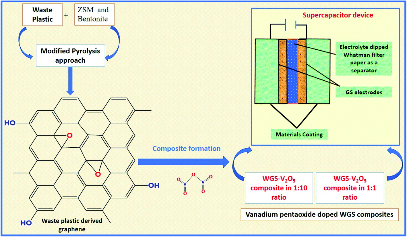 | ||
| Fig. 1 Pictorial representation of the process. | ||
2. Materials and method
2.1. Materials
Waste plastic was collected from the local municipality of Nainital, Uttarakhand, India. All chemicals, such as the brown/yellow solid powder crystalline form of V2O5 (molecular weight 181.88 g mol−1), N-methyl-2-pyrrolidone (NMP), polyvinylidene fluoride (PVDF), graphite sheets (GS), H3PO4, Whatman filter paper, ZSM, and bentonite clay were purchased from Aldrich, and used as received.2.2. Synthesis of graphene sheets
The collected waste plastic was then chopped into small pieces using a shredder. Subsequently, the chopped WP pieces were washed thoroughly by soap solution to remove the impurities from the sample. The shredded WP was mixed with a catalyst, i.e., ZSM and bentonite clay (in a 1:1 ratio) thoroughly. After mixing with the catalyst, the sample was processed for the first stage of pyrolysis, where the sample was placed in a pyrolysis reactor under an inert atmosphere of N2 at the temperature of 370 °C for the next 2 hours. At this stage, the lower hydrocarbon present in WP condensed to form gases, and the higher hydrocarbons condensed in the form of wax and fuels. However, carbon char was also produced along with gases and fuels. After the first step of pyrolysis, which is also known as slow pyrolysis, the second step of pyrolysis was performed to exfoliate the carbon char and to obtain the final product, i.e., graphene sheets. To do so, the carbon char was placed into a secondary pyrolysis reactor at the temperature of 918 °C with the continuous heating rate of 10 °C min−1 under an inert atmosphere of N2 for the next 2.5 hours. The obtained product was then ball-milled properly for several hours, and further washed by double-distilled water many times. At last, after oven drying for a few hours, the final product was obtained. All the characterizations and experiments were performed using that same material.
2.3. Development of the V2O5/WGS composites
The properly washed and dried graphene sample was used for the preparation of V2O5/WGS composites of different mass loadings, i.e., 1:10 and 1:1 ratios. In brief, two beakers were filled with 30 ml DDW each, and 1 g of WGS powder was mixed in both beakers. These beakers were labeled as beaker no. 1 and beaker no. 2. Then, 10 g and 1 g of V2O5 powder were mixed in 50 ml of double-distilled water (DDW) in two different beakers of 200 ml capacity. These beakers were labeled as beaker no. 3 and beaker no. 4, respectively. For the proper mixing of each sample (beakers 1, 2, 3, 4), continuous stirring for 1 h was performed with a magnetic stirrer at a fixed magnet speed of 800 rpm. Furthermore, these samples were placed in a sonicator for the next 1 h, which uses sound waves of high energy to disperse the particles of WGS into DDW uniformly, resulting in a good distribution of the solution. The sonicated solutions were processed through the ultrasonic homogenizer for the next 45 minutes. The ultrasonicated solution of beaker no. 1 was then mixed with an ultrasonicated solution of beaker no. 3. Similarly, the ultrasonicated solution of beaker no. 2 was mixed with the ultrasonicated solution of beaker no. 4. After mixing these solutions, we obtained two different solutions and the samples were labeled as sample A (sample with 1:10 ratio), and sample B (sample with 1:1 ratio). Both solutions were each treated in an intense ultrasonic homogenizer for the next 1 h at high power. The ultrasonic homogenizer disrupts the graphene layers through cavitation, with the ultrasonic waves resulting in a more uniform mixing of the graphene matrix and metal oxide. The obtained solutions (samples A and B) were then processed through the hydrothermal procedure and placed into a Teflon autoclave of 100 ml each for the next 30 h in an oven at 220 °C. After the process, each hydrothermal reactor was cooled to room temperature, and the obtained materials were washed using a centrifuge at 7000 rpm for 15 minutes at a temperature of 25 °C to remove the presence of unnecessary impurities. Finally, the obtained materials were dried in an oven at 90 °C overnight each, and the obtained samples were labeled as WGSA (for the sample with a 1:10 ratio of WGS and V2O5), and WGSB (for the sample with a 1:1 ratio of WGS and V2O5).
3. Characterization
3.1. Material characterization
The prepared samples were then characterized by advanced spectroscopic techniques, such as Raman spectroscopy, Fourier-transform infrared spectroscopy (FT-IR), and X-ray diffraction spectroscopy (XRD). Thermogravimetric analysis (TGA) was carried out in a PerkinElmer TGA-4000 with a heating rate of 5 °C min−1 from 25 to 800 °C under constant nitrogen flow. Transmission electron microscopy (TEM) was used to evaluate the internal morphology of the sample. TEM microscopy was performed on a JEOL JEM 2100 Plus instrument. Meanwhile, scanning electron microscopy (SEM) and energy dispersive X-ray analysis (EDX) were performed on a Carl Zeiss Model Supra 55 instrument for the detection of the surface morphology elemental compositions of the samples. Raman spectroscopy was performed using a Horiba Japan Xplora Plus, which has a 532 nm excitation beam. A PerkinElmer-based Fourier-transformation infrared spectroscopy (FT-IR) C94012 instrument was used for functional group analysis. XRD was performed using the Panalytical X'Pert Pro with a Cu Kα source and excitation beam wavelength of 1.54 Å. The XPS was performed using a VG Scientific ESCA LAB Mk-II Spectrometer.3.2. Device fabrication
To evaluate the electrochemical performance of each device, the supercapacitor electrodes were fabricated using both samples. The WGSA powder and polyvinylidene fluoride (PVDF) are separately mixed in DDW and N-methyl-2-pyrrolidone (NMP), respectively, and mixed overnight on a magnetic stirrer. Furthermore, a mixer was formed using 95 wt% WGS powder and 5 wt% polyvinylidene fluoride (PVDF) in the ratio of 95:5. The obtained mixture was properly mixed to form a slurry using a mortar and pestle, which was then used for the coating of the supercapacitor device. Graphite sheets (GS) of 1 × 1 cm2 area were then pasted using this material, and each electrode was coated with around 1 mg of sample. Furthermore, these electrodes were evaporated overnight in an oven at 90 °C.
Then, a thin film was prepared using a Whatman filter paper (WFP) of 1 × 1 cm2 area and dipped into 1 M H3PO4 (electrolyte solution). A sandwich was prepared by placing WFP in-between the two coated WGS-electrodes. In this structure, WFP plays the role of the separator and 1 M H3PO4 serves as the electrolyte (Scheme 1). A similar procedure was used for the device fabrication using the WGSB sample. A diagram of the device fabrication is given in Scheme 1, along with the device structure in Table 1.
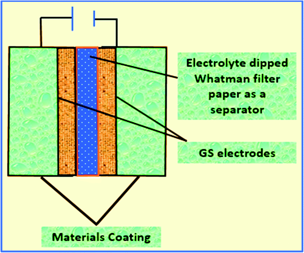 | ||
| Scheme 1 Fabrication of the electrode device. | ||
| Cell | Device structure |
|---|---|
| Cell 1 | GS|WGSA|electrolyte dipped WFP|WGSA|GS |
| Cell 2 | GS|WGSB|eElectrolyte dipped WFP|WGSB|GS |
3.3. Device characterization
The fabricated device was processed for two-electrode system-based electrochemical performance testing in the Metro-Ohm Autolab PGSTAT204. Cyclic voltammetry (CV), GCD, and EIS were performed. The CV was performed at different scan rates, i.e., 5 mV s−1, 10 mV s−1, 50 mV s−1, 100 mV s−1, 200 mV s−1, and 500 mV s−1, using 1 M H3PO4 as the electrolyte. The charge/discharge was performed at different current densities, viz., 1 A g−1, 2 A g−1, and 3 A g−1, over the potential window of 0–1 V. Electrochemical impedance spectroscopy (EIS) analysis was performed at the range of 10 mHz to 106 Hz.4. Results and discussion
Graphene synthesis was confirmed using different advanced characterization techniques, such as Raman spectroscopy, FT-IR spectroscopy, XRD analysis, thermogravimetric analysis (TGA), and UV-visible spectroscopy. Along with this, the surface morphology of the graphene sheets was evaluated by scanning electron microscopy (SEM). Furthermore, the doping of vanadium pentaoxide onto the graphene sheets was confirmed by FT-IR spectroscopy and UV-visible spectroscopy.The synthesis of graphene was first confirmed by Raman spectroscopy, which is the most prominent technique for the identification of graphene. Raman spectroscopic details of the synthesized material showed D, G, and 2D bands at 1336 cm−1, 1534 cm−1, and 2822 cm−1, respectively. These bands are due to in-plane and out-of-plane vibrations that confirm the presence of the basic structure of graphene in the carbonic structure. The presence of excellent D and G bands with an ID/IG ratio of around 0.87, and a 2D band at 2822 cm−1 with an I2D/IG ratio of 1.8, confirms the synthesis of few-layered graphene sheets. The presence of the D band belongs to the deformative vibration, which arose due to the breaking down of the carbonic double bonds mainly by the conversion of sp2-hybridization to sp3-hybridization.16–21 The G band at 1534 cm−1 also confirmed the presence of unsaturated carbon atoms in the graphene sheets. The presence of the D band at 1336 cm−1, along with an I2D/IG of 1.8, depicts the existence of oxidative defects in WGS. However, the out-of-plane vibration causing the D band and in-plane vibration causing the G band indicate the contributing conversion of sp2 into sp3 hybridization, and result in the presence of edge dislocation defects or other possible structural defects in WGS.22,23 Our quantum mechanical evaluation predicts that the second-order Raman spectrum that arose due to the interface between two phonons near the K-point is responsible for the appearance of the D band.23 The elastic scattering also appeared due to the presence of defects, and the emission or absorption of the phonon responsible for the appearance of inelastic scattering in the D band of WGS near the K-point.23 The lower intensity of the D band shows that the reduced degree of sp3 hybridized carbon atoms may be due to defects and oxidizing sides. However, the higher degree of the G band confirms a greater shift of sp2 into sp3 hybridization, which ultimately confirms the presence of more saturated carbons in the graphene skeleton. A doubly degenerated, E2g phonon symmetry mode vibration of the first-order Raman scattering in the middle of the Brillouin zone is very much responsible for the appearance of the G-band.25,26 The single-layered graphene usually shows an I2D/IG ratio of 0.5, as the distortion, dislocation, and more oxidative site shows the carbonic skeleton with few-layered graphene sheets, thus showing the synthesis of 3–4 layered graphene (Fig. 2a).
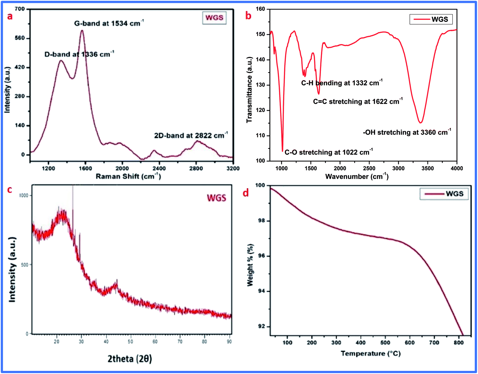 | ||
| Fig. 2 (a) Raman spectrum of WGS. (b) FT-IR spectrum of WGS. (c) XRD analysis of WGS. (d) TGA analysis of WGS. | ||
Furthermore, the FT-IR spectrum of WGS showed the presence of few oxygenic and non-oxygenic functional groups, like C–O, C–H, C![[double bond, length as m-dash]](https://www.rsc.org/images/entities/char_e001.gif) C, and –OH at 1022 cm−1, 1332 cm−1, 1622 cm−1, and 3660 cm−1, respectively (Fig. 2b). These peaks arose due to the stretching vibration between the different hybridizing groups of carbon and oxygen.16–21 The FT-IR spectrum of WGS showed the presence of epoxy, CC, C–H, and –OH stretching vibrations,20 which reinforces the Raman spectrum of WGS. The FT-IR data were reinforced by XRD and TGA analysis, which showed the presence of concentrated oxygenic sites (Fig. 2c and d).
C, and –OH at 1022 cm−1, 1332 cm−1, 1622 cm−1, and 3660 cm−1, respectively (Fig. 2b). These peaks arose due to the stretching vibration between the different hybridizing groups of carbon and oxygen.16–21 The FT-IR spectrum of WGS showed the presence of epoxy, CC, C–H, and –OH stretching vibrations,20 which reinforces the Raman spectrum of WGS. The FT-IR data were reinforced by XRD and TGA analysis, which showed the presence of concentrated oxygenic sites (Fig. 2c and d).
Additionally, the XRD analysis of WGS showed the presence of two broad crests at 2θ = 16°–20° and another at 2θ = 40°–45°. The initial band arose due to the graphitic amorphous nature of the materials, and another one is due to the conversion of the specific crystal structure into a reduced carbonic framework, thus representing the sp3 hybridized carbon atoms plane. The XRD analysis depicts two characteristic peaks, which correspond to the presence of graphene nanosheets. XRD analysis was also used to evaluate the number of layers in WGS using a previously reported method, where the number of layers in the WGS sheets was obtained by dividing the crystal size (C) by the interlayer distance (d) further, which was added into the thickness of a single-layered graphene sheet by assuming a thickness of 0.1 nm. The Scherrer equation was used to calculate the crystal size (C). The interlayer distances (d) were evaluated using Bragg's law,21 and the XRD analysis revealed about 3–4 four layers in WGS.21 These evaluations showed that the XRD data support the above discussed Raman and FT-IR data (Fig. 2a–c). These evaluations were further strengthened by the TGA analysis, which confirmed the thermal stability at the specific mass loss of the materials (Fig. 2d). A weight loss of 4–5% at a temperature below 200 °C confirmed the reduction of unstable functional groups, such as –OH and –CO. This may correspond to the presence of water molecules (Fig. 2d). The presence of these oxidative functionalities was already confirmed by the above-discussed FT-IR spectrum of WGS (Fig. 2b). Additionally, in the one-step decay of materials between 300 °C and 450 °C, the temperature displayed a reduction in the oxidizing groups. Thus, Raman spectroscopy, FT-IR spectroscopy, XRD analysis, and TGA analysis validated the synthesis of the graphene domain-based structure of WGS.
The synthesis of WGS was confirmed with the help of a comparative study of the FT-IR and UV-Vis spectroscopic details, along with a comprehensive discussion of the SEM and TEM data of WGS. The WGS sample showed C–C stretching, C–O–C stretching, C–H bending, CC stretching, and –OH stretching vibrations at 870 cm−1, 1020 cm−1, 1322 cm−1, 1622 cm−1, and 3360 cm−1, respectively (Fig. 3). The FT-IR spectrum of WGSB showed C–C stretching, C–O–C stretching, C–H bending, CC stretching, and –OH stretching vibrations at 518 cm−1, 777 cm−1, 990 cm−1, 1600 cm−1, and at 3404 cm−1, respectively. However, the sample WGSA showed characteristic peaks of C–O–C stretching and –OH stretching vibrations at 1008 cm−1 and 3404 cm−1, respectively (Fig. 3).21–24 Fig. 3 depicts the presence of only two characteristic peaks in the FT-IR spectrum of the WGSA sample, which represents the presence of pi–pi interactions between WGS and the vanadium pentaoxide molecules. However, the reduction in the intensity of the WGSA and WGSB samples is also a clear indication of more bonding interaction between such groups as the bonding interaction results in weakening the respective bonds, which results in lowering the intensity of the related FT-IR vibration. The intensity of the –OH functional group increases in the composite in comparison to the neat WGS sample. This may be attributed to the existence of intermolecular hydrogen bonding between vanadium pentaoxide and the oxidative part of the graphene sheets. Thus, the slightly increased vibration occurred as an increase in the frequency for the FT-IR spectrum.
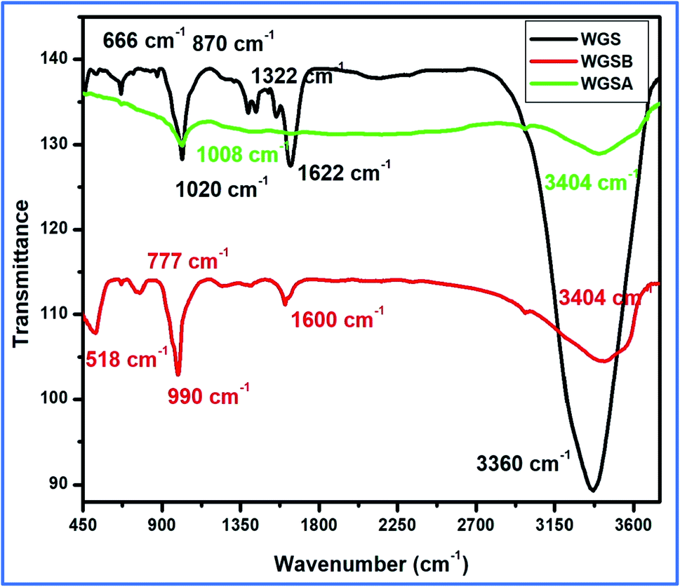 | ||
| Fig. 3 FT-IR spectra of the WGS, WGSA, and WGSB samples. | ||
This rise can be attributed to the direct correlation between the FT-IR spectrum and the stretching of bonds. The greater the stretching of a bond, the greater the energy required to break it. Thus, the frequency to break such bonds will also be greater, as the frequency can be correlated with the force constant of a bond using eqn (1):
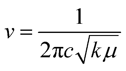 | (1) |
Thus, from eqn (1), it becomes clear that the –OH vibration comes in a higher range in WGSA and WGSB compared to the WGS sample due to the appearance of higher bonding forces in these samples.
This can also be attributed to the existence of partial resonance, which exists in the graphene ring structure due to the partial H-bonding based interaction between vanadium pentaoxide and the –OH functionality of the partially oxidized graphene. Additionally, the lack of carbonyl functionality in the WGSA composite and decrement in the intensity of the same vibration at 1600 cm−1 indicated the slight reduction from its original roots in WGS, which was around 1622 cm−1. This can be attributed to the absence of the CC vibration in the WGSA, which was due to the presence of π–π interactions and the hydrogen bonding between the polar moieties of WGS and the vanadium pentaoxide molecules (Fig. 3).16,21–25 The π–π interactions and the hydrogen bonding typically interrupt the bond strength and length. Thus, these bonds become a charge-fluctuating and directionless moiety, resulting in poor FT-IR peaks at such points.
FT-IR results showed the peak shifting and peak depletion of the C–O–C stretch, CC stretching vibration, and O–H stretching vibrations from its original peaks in WGS at 1020 cm−1, 1622 cm−1, and 3360 cm−1, respectively. The FT-IR data validate the presence of oxidative functionalities to some extent, and also clarify the formation of WGS, WGSA, and WGSB, in addition to the XRD analysis, Raman spectroscopy, and TGA analysis. The formation of WGSA and WGSB was also confirmed by the UV-Vis spectroscopic results, along with the bandgap analysis (Fig. 4).
 | ||
| Fig. 4 (a) UV-Vis spectra of the WGS, WGSA, and WGSB samples. (b) Indirect bandgap of WGS. (c) Direct bandgap of WGS. | ||
The UV-Vis spectrum showed the peak corresponding to the CC bonds-based π–π* transitions of the unsaturated WGS system at 238 nm wavelength. The electronic π–π* transitions in the composites, i.e., WGSB and WGSA, showed a reduction in the peak intensity and increment in the peak absorption, which confirmed the formation of the WGSA and WGSB composites. The UV-Vis spectrum strengthened the FT-IR data for the synthesis of composites. The UV data also support the synthesis of graphene, as explained by the Raman spectrum, FT-IR data, XRD analysis, and TGA analysis.
Furthermore, the electronic π–π* transitions of the WGS-based composite showed an excellent absorption pattern, which was used for the determination of the direct and indirect bandgaps in the material. Based on the absorption pattern of the UV-Vis spectra, the Tauc plot was evaluated using the following eqn (2):
| (αhν)2 = A(hν − Eopt) | (2) |
 | ||
| Fig. 5 The pictorial representation of the bandgap and graphene framework in WGS. | ||
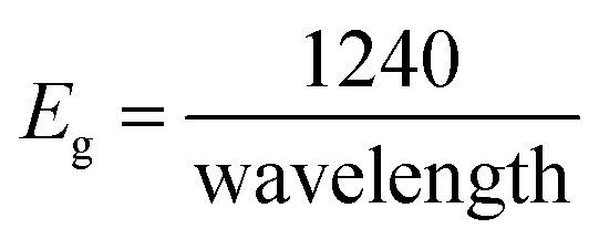
The lower bandgap depicts the excellent candidature of the synthesized materials as an active electrode material for the energy storage devices. Eg can be calculated using the following eqn (3):
 | (3) |
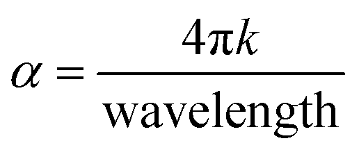
Furthermore, the value of the (α) optical absorption coefficient can be calculated using eqn (4):
 | (4) |
After calculating these values, we can plot the graph of (αhν)2 vs. energy (hν) for the evaluation of the direct and indirect bandgaps in WGS, where the straight-line interception to the curve on the X-axis provides the value of the optical bandgap. After evaluating the interceptions of this curve, we obtained a direct bandgap of 2.45 eV and indirect bandgap of 1.45 eV for WGS. These direct and indirect bandgaps depict the excellent potential of the WGS-based composite materials for energy storage applications, which was evaluated using cyclic voltammetry (CV). A lower bandgap can be correlated with the energy splitting between the bonding and antibonding orbitals, which decreases as the bonds become weaker.
Furthermore, the FE-SEM image of WGS showed a sheets-shaped structure, which can be seen in Fig. 6a. Fig. 6b shows the external edge-based layer count in the SEM image of WGS, and depicts the 2–3 layers' presence on the edges of the WGS. Fig. 6c shows the layers intensity-based histogram plot of the SEM image, which represents the weight and amount of surface captured in specific areas of the SEM plot, along with the standard deviation and mean count value of most mass accumulation. Fig. 6d shows the 3D plot profile of the SEM image. The 3D plot profile shows the fibrous surface of the graphene sheets, as shown in Fig. 6d. The SEM analysis evaluated the external morphology of WGS. Fig. 6a–d shows the sheets-shaped structure of WGS. However, the plot profile of the SEM image depicted the spherical pattern surrounded by valves in the internal structure of WGS, which may be reflected in the presence of oxidative sites and edge dislocation-based defects (Fig. 6d). Fig. 6c shows the SEM layer's intensity-based histogram plot. Fig. 6d depicts the surface profile interactive surface plot of WGS. This plot profile diagram-based evaluation shows the average thickness of the WGS image and confirms the synthesis of the two-three layered graphene sheets. Moreover, the synthesized WGS-based composites were used as the active electrode material for the fabrication of supercapacitor electrodes.
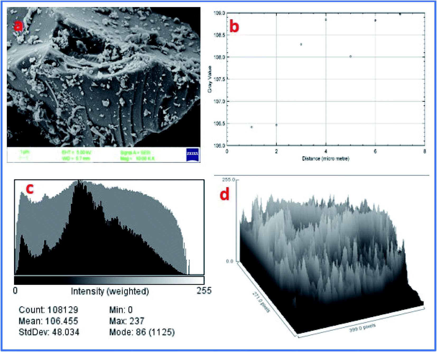 | ||
| Fig. 6 (a) FE-SEM image of WGS. (b) Surface layer count in the data plot of SEM. (c) Layer intensity-based histogram plot of the SEM image. (d) Plot profile of the SEM image. | ||
Furthermore, SEM imaging of the WGSA and WGSB samples (Fig. 7a and b) was done to find out the interactive surface behavior of both samples. The SEM image of WGSA showed agglomerative behavior of the developed composite, where the flake-shaped structure depicted the presence of V2O5 in the composite. The spherical-shaped SEM image of the WGSA composite material depicted the presence of excellent interaction between both materials of the composite. However, the interaction between both materials was randomized in WGSB, as the flake-shaped structures turning into fibrous flakes might be due to random interactions during the mixing of materials. The sheets-shaped structure of WGS (Fig. 6a) first turned to agglomerated flake sheets in WGSA, and finally into fibrous flakes-based sheets in WGSB, which depicts the fine structural conversion in the developed material. These structural changes are visible in the structure of WGS (Fig. 6a), WGSA (Fig. 7a), and WGSB (Fig. 7b).
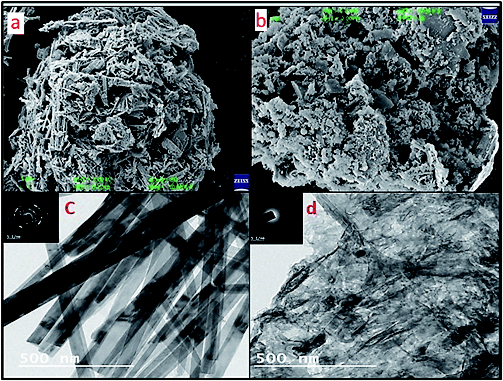 | ||
| Fig. 7 SEM images of (a) WGSA and (b) WGSB, and TEM images of (c) WGSA and (d) WGSB. | ||
The SEM data were further strengthened by TEM images, as shown in Fig. 7c and d. Fig. 7c depicts a sharp rod shape structure of vanadium pentaoxide, and the dark area in the image depicts the successful doping of graphene. However, Fig. 7d represents the WGSB sample with an equal ratio of vanadium pentaoxide and graphene. Thus, the clear distribution of graphene over the whole area of the vanadium oxide surface can be seen. TEM images at 5.1 nm (Fig. 7c) display the SAED pattern for WGSA, showing the distributed pattern. Meanwhile, a similar but more diverse SAED pattern can be seen for WGSB in Fig. 7d. The images at 500 nm show a clear depiction of the excellent interaction between both reacting moieties. The spotted dark areas in the TEM images of both samples depict graphene sheets, while the rod-shaped structures can confirm the presence of vanadium oxide. These magnifications of the TEM images are sufficient in providing a clear picture of the internal structure of both samples.
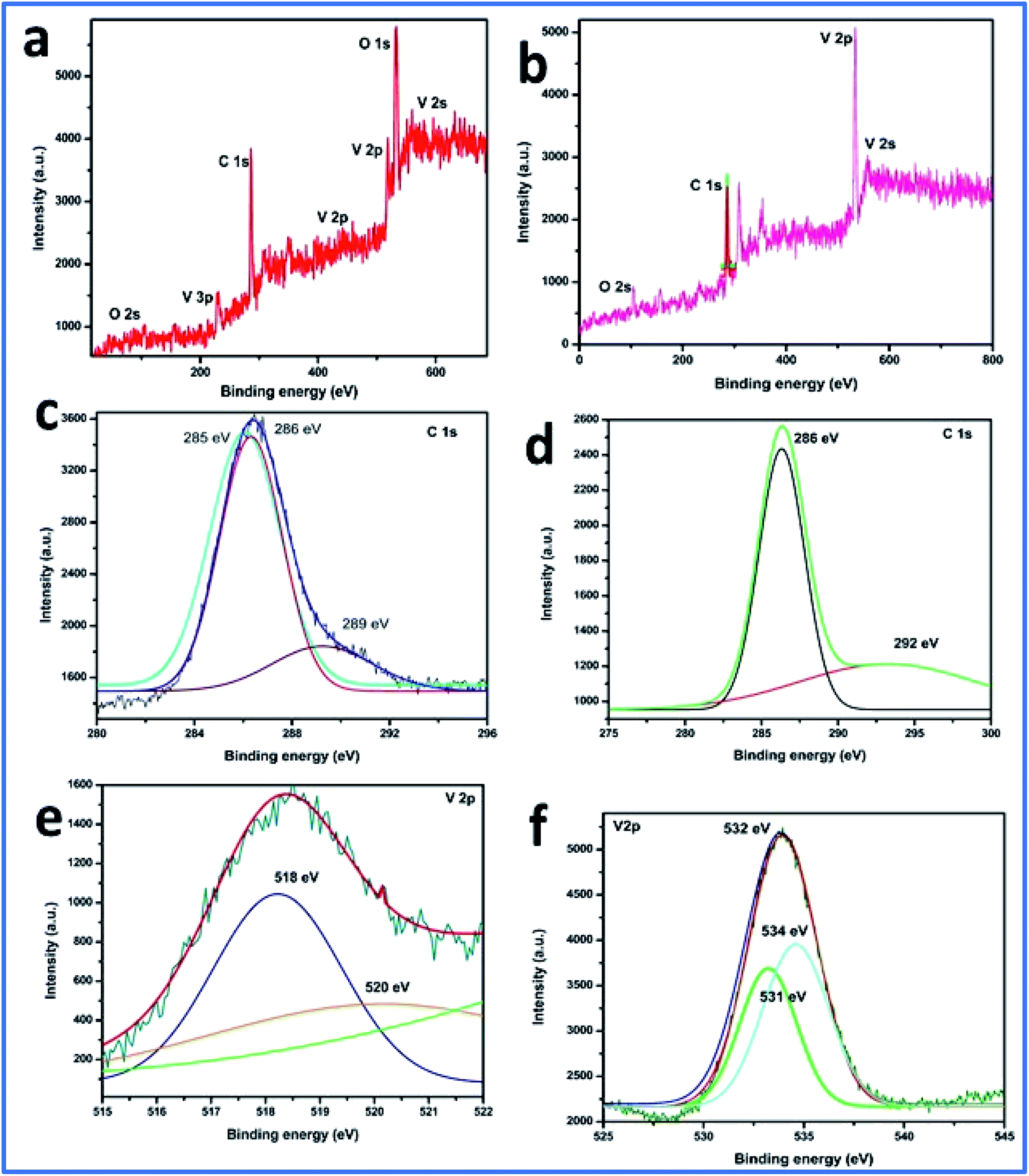
Furthermore, the SEM and TEM data were supported by the EDX data, which was used for evaluating the elemental composition of carbon and vanadium in the WGSA and WGSB samples. The EDX spectrum of WGSA is visible in Fig. 8a, while the EDX spectrum of WGSB is visible in Fig. 8b. Similarly, the tabulated elemental composition of both samples (WGSA and WGSB) is depicted in Fig. 9a and b, respectively. The EDX data depicted the apparent concentration of carbon and vanadium in both samples. Sample WGSB depicted the presence of a low weight percentage of vanadium, and the EDX spectrum of WGSA depicted a high weight percentage of vanadium in the sample (Fig. 8a, b, 9a and b). Thus, the SEM and EDX data confirm the presence of vanadium in low and high weight percentages in samples WGSA and WGSB, respectively. Additionally, XPS was performed for both samples (Fig. 10). The distinctive peaks of the chemical bonds between carbon, oxygen, and vanadium oxide appeared at their corresponding binding energies, as demonstrated in the XPS survey scan (Fig. 10). However, the distinctive XPS peaks for WGSA at 218 eV, 285 eV, 518 eV, 530 eV, and 580 eV are assigned to the V 3p, C 1s, V 2p, O 1s, and V 2s, respectively. Similarly, the sample WGSB showed peaks at 128 eV, 286 eV, 532 eV, and 560 eV, for O 2s, C 1s, V 2p, and V 2s, respectively. The C 1s high-resolution spectrum was also deconvoluted into a main Gaussian curve centered at 285 eV and 286 eV for WGSA and WGSB, respectively (Fig. 10c and d). The XPS spectra of both samples indicate that V2O5/WGS contains only C, V, and O, corresponding to the different aforementioned peaks. The high-resolution XPS spectra in Fig. 10e and f show the V 2p peaks for WGSA and WGSB at 518.0 eV, 520 eV, 531 eV, 532 eV and 534 eV, which is attributed to the V–C–O bond.14,19 The peaks at 520.9 eV, 531 eV, and 534 eV can also be attributed to V3+, V4+, and V5+, respectively. The presence of V4+ and V5+ in the samples is a result of the air oxidation of the V2O5 surface.19
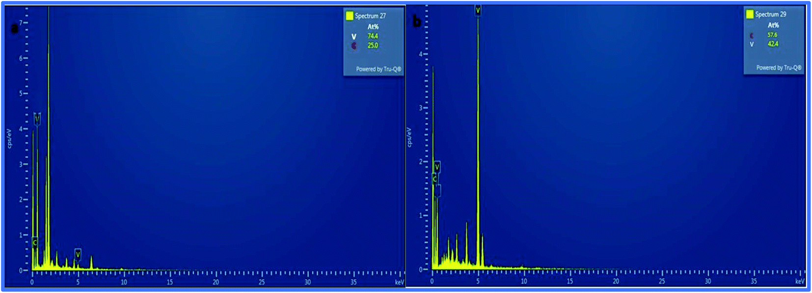 | ||
| Fig. 8 EDX spectra of (a) WGSA and (b) WGSB. | ||
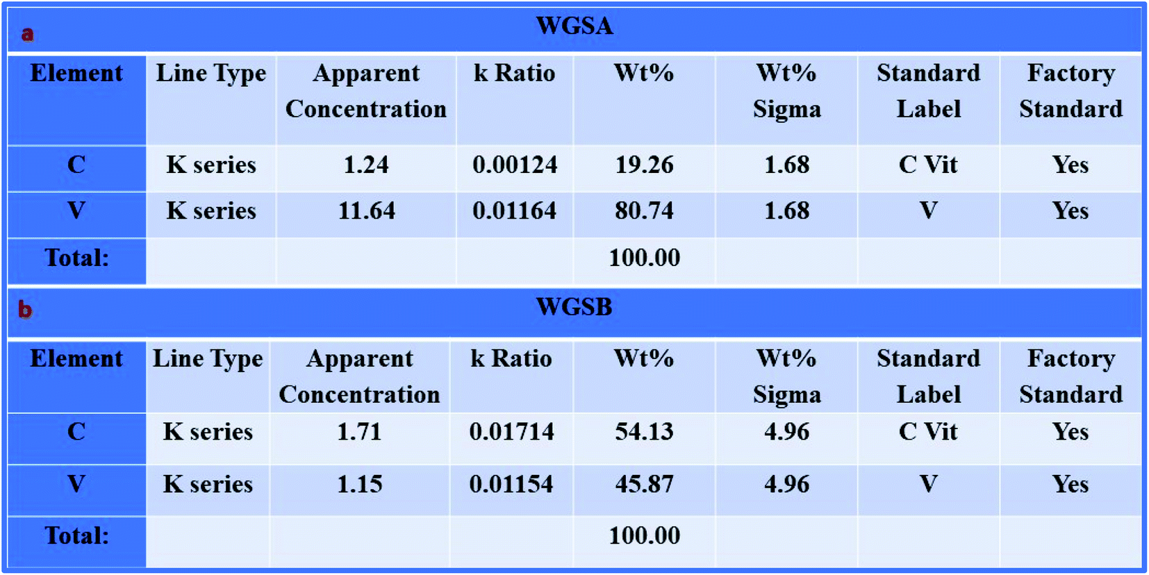 | ||
| Fig. 9 EDX-based elemental composition of (a) WGSA and (b) WGSB. | ||
 | ||
| Fig. 10 XPS data of both samples. (a) XPS survey scan spectra of the WGSA composite. (b) XPS survey scan spectra of the WGSB composite. (c) C 1s spectra of WGSA. (d) C 1s spectra of WGSB. (e) V 2p spectra of the WGSA composite. (f) V 2p spectra of the WGSB composite. | ||
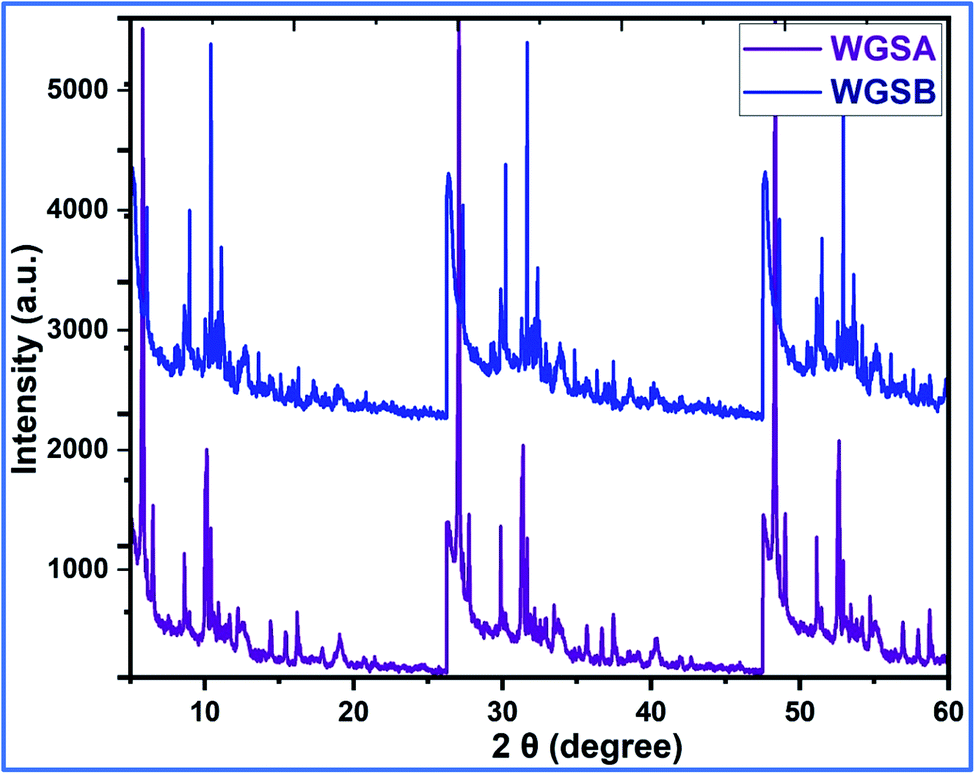
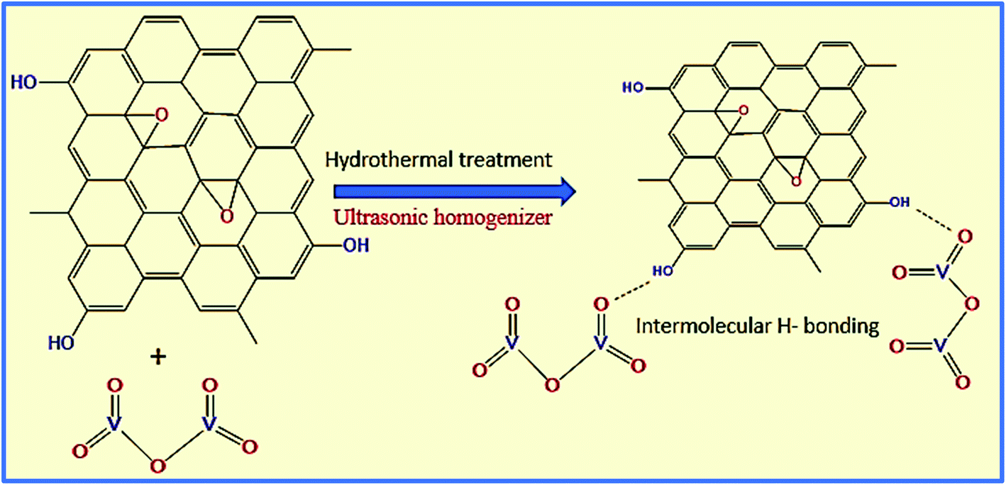
Next, the WGSA and WGSB samples were evaluated by XRD analysis to find out the relative peaks of vanadium and the presence of crystallinity in the samples (Fig. 11). The XRD data of WGSA and WGSB are shown in violet and blue colors, respectively, in the XRD curve given in Fig. 11. However, both samples WGSA and WGSB show the presence of nearly identical characteristic peaks. The only difference is the intensity and acuity of these peaks in both samples. The diffraction peaks at different planes with 2θ equal to 15°, 26°, 28°, 32°, 48°, and 52° correspond to the 001, 110, 111, 004, 060, and 061 planes, respectively. Thus, they can be assigned to the existence of vanadium pentaoxide in both materials.27–30 Yet, the sample WGSA shows quite sharp and high-intensity peaks in comparison to the XRD peaks of WGSB, which can be attributed to the presence of a more crystalline composition in sample WGSA attributed to the high presence of vanadium pentaoxide in the material. Slightly broad peaks at 2θ = 10°, 2θ = 15°, and 2θ = 40°–42° can be assigned to the presence of WGS in the material, as the peaks at this range arise due to the presence of the graphitic skeleton.27–29 The XRD pattern is quite similar to the results previously reported by Jin et al.,25 Qin et al.,26 and Chen et al.27 These results reveal that the broader area of the XRD pattern is responsible for the amorphous nature of the material due to the graphitic skeleton. However, the sharp peaks are the characteristic peaks of metal oxides or crystalline substances, and can be assigned to the presence of vanadium pentaoxide in the material. Furthermore, the growth mechanism for the development of the graphene–vanadium pentaoxide composite based on FT-IR, UV, XPS, and XRD data is given in Scheme 2. The development of the graphene–vanadium oxide composite was developed due to the presence of intermolecular hydrogen bonding between both moieties. The interactions were also confirmed by FT-IR spectroscopy, XRD spectroscopy, SEM/EDX analysis, TEM analysis, and XPS analysis.
 | ||
| Fig. 11 XRD analysis of WGSA and WGSB. | ||
 | ||
| Scheme 2 The growth mechanism for the development of the graphene/vanadium oxide composite. | ||
4.1. Electrochemical performance testing
The developed WGSA and WGSB samples were used as the active electrode material for the electrode device fabrication. The fabricated device was evaluated by cyclic voltammetry (CV), galvanic charge–discharge (GCD), and electron impedance spectroscopy (EIS). The CV data of the fabricated cells (Table 1) showed impressive characteristics over the performed voltage range of 0 to 1 V, and at the scan rate of 5 mV s−1, 10 mV s−1, 50 mV s−1, 100 mV s−1, 200 mV s−1, and 500 mV s−1 using 1 M H3PO4 as the electrolyte. The cell structure and configuration are given in Scheme 1 and Table 1. The specific capacitance calculated via each CV curve is shown in Table 2 for cells 1 and 2.| Scan rates (in mV s−1) | 5 | 10 | 50 | 100 | 200 | 500 |
|---|---|---|---|---|---|---|
| Cs of cell 1 (in F g−1) | 139.7 0 | 98.00 | 74.30 | 51.60 | 40.00 | 26.10 |
| Cs of cell 2 (in F g−1) | 51.30 | 42.80 | 36.90 | 23.00 | 16.00 | 6.80 |
CV was performed in a two-electrode system at different scan rates using 1 M H3PO4 as the electrolyte, and WFP was used as the separator between the electrodes. The CV plot is a plot between the applied current (A) and potential (V). In the case of cell 2, a traditional electric double-layer capacitor (EDLC) type of behavior of the curve was observed. However, for cell 1, some distortion in the curve can be observed (Fig. 12a and b). The distortion can be attributed to the high mass loading of vanadium pentaoxide onto WGS sheets, which resulted in pseudocapacitance in the developed composite. Thus, the distortion from the ideal EDLC behavior can be seen in cell 1. However, cell 1 followed a pseudo redox mechanism for the storage of ions at the exchange, which results in the relative storage of the capacitance. Cell 2 followed the electric double layer formation at the interface of the material and electrolyte ions, which is responsible for the relative transportation of ions for performing the charge storage mechanism. However, the reactions occurring in the graphene–vanadium oxide composite at the electrode are shown below:32,33
| V2+ ⇄ V3+ + e− | (5) |
| VO2+ + e− + 2H ⇄ VO2 + H2O | (6) |
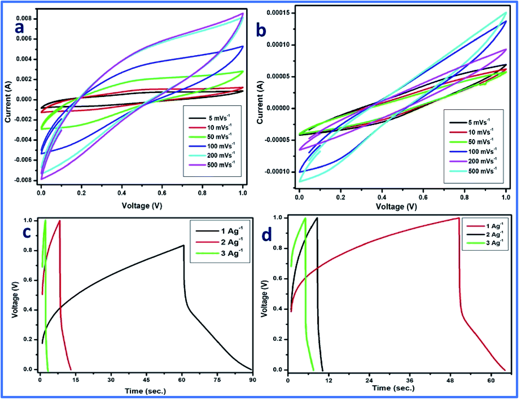 | ||
| Fig. 12 Cyclic voltammetry of (a) WGSA and (b) WGSB. GCD plots of (c) WGSA and (d) WGSB. | ||
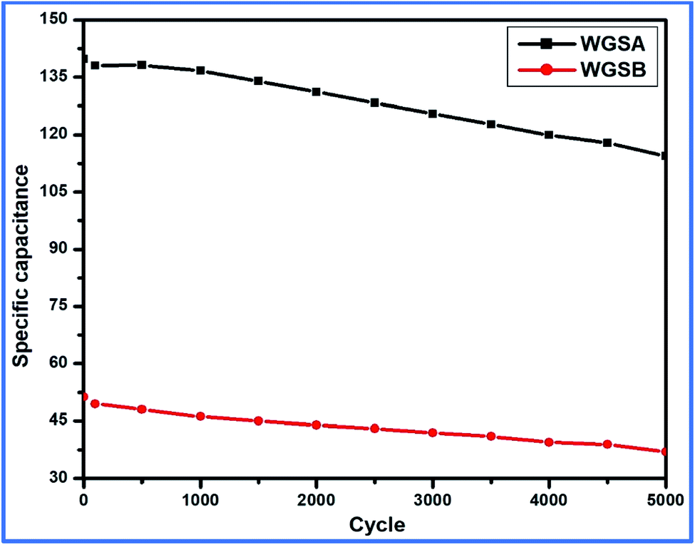 | ||
| Fig. 13 Cyclic stability of WGSA and WGSB up to 5000 cycles. | ||
The specific capacitance was calculated using eqn (7), and the specific capacitance related to each cell is shown in Table 2. Furthermore, the evaluations related to the specific capacitance were studied over different scan rates, suggesting excellent stability of both cells, especially cell 1 with increasing scan rates (Table 2):16,25
 | (7) |
Furthermore, the energy densities were calculated for cells 1 and 2 using eqn (8), and their values are given in Table 3:
 | (8) |
| Scan rates (in mV s) | 5.00 | 10.00 | 50.00 | 100.00 |
|---|---|---|---|---|
| ED of cell 1 (in W h kg−1) | 19.70 | 13.60 | 10.80 | 7.20 |
| PD of cell 1 (in W kg−1) | 5312.36 | 4730.43 | 4182.69 | 3600.00 |
| ED of cell 2 (in W h kg−1) | 7.20 | 5.90 | 3.20 | 2.30 |
| PD of cell 1 (in W kg−1) | 1941.00 | 1872.00 | 1232.08 | 1089.47 |
The power density (PD) was also calculated for each cell using eqn (9). Cell 1 showed the highest power density of 5312 W kg−1, and cell 2 showed the highest power density of 1941 W kg−1.31,34
 | (9) |
Thus, cell 1 with the highest energy density of 19.7 W h kg−1 and power density of 5312 W kg−1 emerged as the superior device in comparison to cell 2, which shows the highest energy density of 7.2 W h kg−1 and power density of 1941 W kg−1 (Fig. 13).
Additionally, galvanic charge–discharge (GCD) analysis was performed for both cells to understand the cyclic stability and the charging–discharging behavior at current densities of 1 A g−1, 2 A g−1, and 3 A g−1 over the wide potential range of 0–1 V (Fig. 12c and d). The charge–discharge plot of cells 1 and 2 showed nearly triangular charging and discharging behavior of each cell. This confirmed the excellent charge storage behavior of these devices. Furthermore, the capacitative performance of both cells was tested by GCD using eqn (10) given below, and the findings are tabulated in Table 4.
 | (10) |
| Current density (in A g−1) | 1 | 2 | 3 |
|---|---|---|---|
| Cs of cell 1 (in F g−1) | 58.15 | 33.40 | 19.00 |
| ED of cell 1 (in W h kg−1) | 8.07 | 4.63 | 2.63 |
| PD of cell 1 (in W kg−1) | 968 | 1386 | 1567 |
| Cs of cell 2 (in F g−1) | 17 | 10 | 9 |
| ED of cell 2 (in W h kg−1) | 2.36 | 1.38 | 1.25 |
| PD of cell 2 (in W kg−1) | 499 | 993 | 1499 |
Based on the above-tabulated data (Table 4), it is very clear that cell 1 has better electrochemical potential in comparison to cell 2. Furthermore, the cyclic stability of each cell was tested on a charge–discharge plot up to 5000 cycles, and is shown in Fig. 10. Cell 1 showed 82% retention in specific capacitance up 500 cycles. However, cell 2 showed up to 73% retention of cycle life. Higher retention of specific capacitance of the WGBA sample might be correlated to the existence of admirable interaction between WGS and the metal oxide ions that are relatively lower in the case of the sample WGSB (Fig. 12).
Moreover, electrochemical impedance spectroscopy (EIS) was used for the detection of equivalent sheet resistance (ESR) on cells 1 and 2. The evaluations were performed at 10 MHz (Fig. 14). The Nyquist plot revealed the impedance of the devices, which was obtained by plotting the imaginary part of the impedance against the real parts of the impedance.
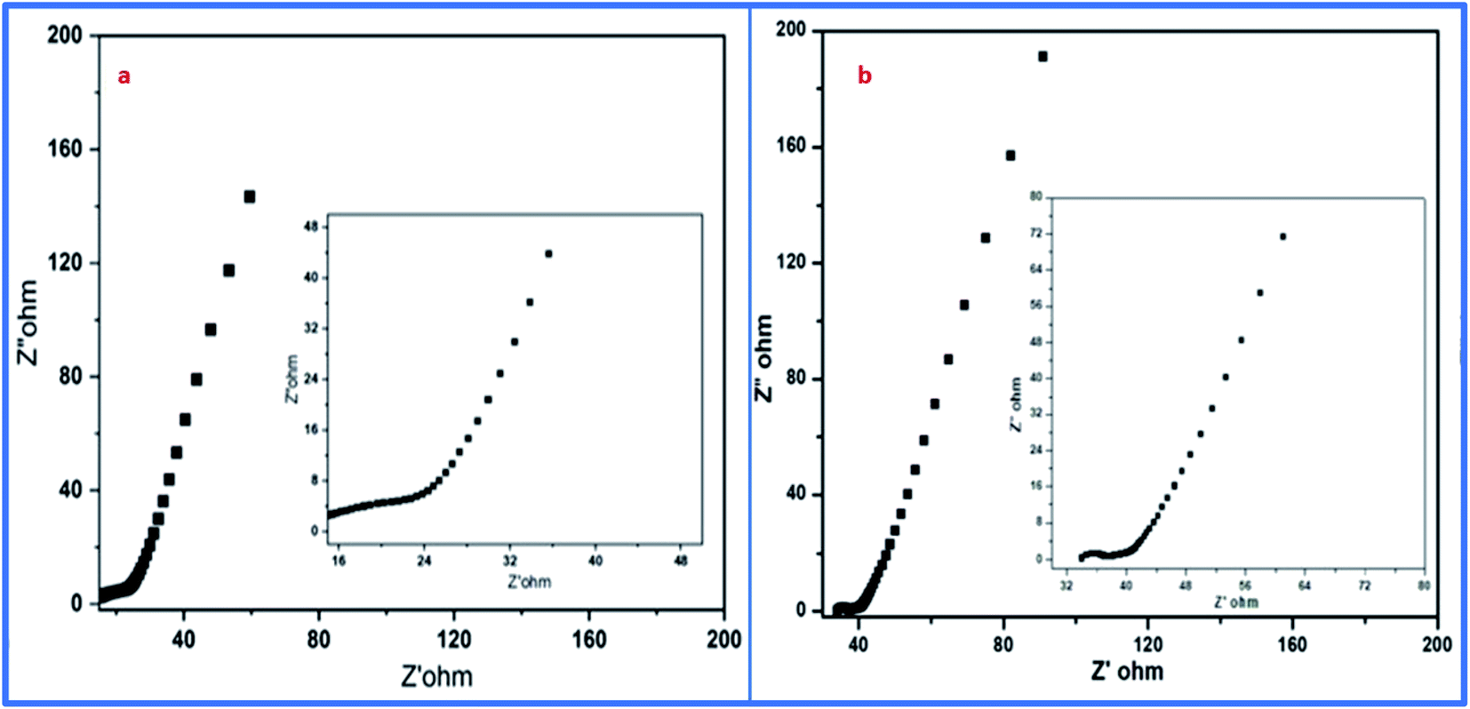 | ||
| Fig. 14 EIS-based Nyquist plots of (a) WGSA and (b) WGSB. | ||
The initial steep increase in the plot around the lower frequency region represents the capacitative behavior of both cells. The ESR of 6.3 Ω cm−2 was obtained from the Nyquist plot of cell 1. Meanwhile, for cell 2, it was evaluated to be about 32.2 Ω cm−2. This represents the restricted transportation of ions due to ESR, which holds fast conduction of ions in the electrolyte for cell 2. This can be outlined as the basic reason for the depletion of specific capacitance in cell 2 in comparison to cell 1. The lower value of ESR results in higher electronic conditions and lower impedance of the circuit. This affects the overall performance of cells in terms of their stability, capacitance, and transportation of ions around the interface of the electrolyte and electrode materials. Furthermore, the electrochemical performance of both samples was evaluated using a three-electrode system, where platinum wire acted as a current collector electrode, while Ag/AgCl was used as a reference electrode, and the glassy carbon was used as the working electrode in 1 M H3PO4 as an electrolyte. The detailed study is attached and explained in the ESI (Fig. S1, S2 and Table S1†). The three-electrode system-based data evaluation showed a correlation with the results of the two-electrode system. Next, the capacitance behavior of both samples was evaluated by Dunn's method, as the capacitance behavior of a device is divided into two parts, i.e., surface capacitance and diffusion capacitance. The surface capacitance is due to the contribution from the electric double layer at the surface of the material, which follows the faradaic mechanism of charge storage. In the case of EDL capacitance or pseudocapacitance, the response of the current with voltage is linear. Alternatively, in the case of diffusion capacitance, the insertion of electrolyte ions on top of the electrode material shows a redox nature, which corresponds to the battery type behavior and is controlled by the diffusion potential of ions. Due to this diffusion capacitance, the current responds non-linearly to the voltage. However, a practical device can have coexisting capacitance including both types. In such a case, the current can be explained as follows:
| i(V) = k1v + k2v0.5 = is + id | (11) |
| I(V)/v0.5 = k1v0.5 + k2 | (12) |
Furthermore, by plotting the i/v0.5 versus v0.5 plot, the values of the constants k1 and k2 can be easily calculated as the slope and intercept, respectively. These values of constants k1 and k2 can also be used to determine the surface capacitance (Cs) and diffusion capacitance (Cd) of the device. In addition, the samples, WGSA and WGSB were investigated using the aforementioned method at a low scan rate of 1 mV s−1 to 10 mV s−1 using the potential window of 0–1 V (Fig. 14). In particular, we calculated the current arrived from the diffusion capacitance, i.e., id, and the current produced from the surface capacitance, i.e., is, for the scan rate of 1 mV s−1.
The CV curve was also divided into two sections (Fig. 15), where the inner section represents the contribution from the surface capacitance, while the outer part represents the contribution from the diffusion capacitance at the scan rate of 1 mV s−1. The results are shown in Table 5, representing 77.97% contribution of surface capacitance for WGSA, and 55.95% contribution of surface capacitance for the WGSB sample at the scan rate of 1 mV s−1. The results showed a higher contribution of the surface capacitance for both samples at the higher scan rate of 100 mV s−1 (Table 5).
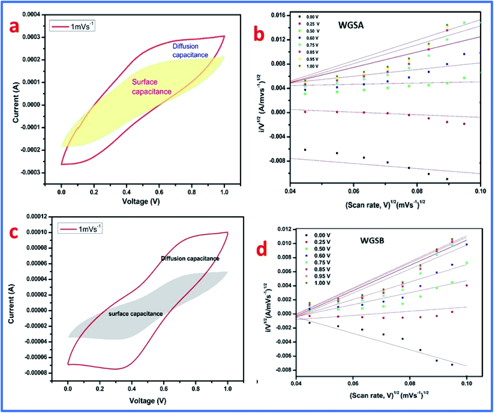 | ||
| Fig. 15 Kinetics of both samples. (a) CV plot of WGSA at 1.0 mV s−1 separated into surface and diffusion capacitances. (b) Plot of i/v0.5 versus v0.5 at different potentials. (c) CV plot of WGSB at 1.0 mV s−1 separated into surface and diffusion capacitance. (d) Plot of i/v0.5 versus v0.5 at different potentials. | ||
| Scan rate | WGSA | WGSB |
|---|---|---|
| a Where Cs is the surface capacitance and Cd is the diffusion capacitance. | ||
| 1 mV s−1 | Cs = 77.97% | Cs = 55.95% |
| Cd = 22.02% | Cd = 44.04% | |
| 100 mV s−1 | Cs = 97.25% | Cs = 88.75% |
| Cd = 2.74% | Cd = 11.25% | |
From this data, it can be concluded that at a higher scan rate, the surface capacitance contributes more than the diffusion capacitance. Quite the reverse, at low scan rates, the contribution of the diffusion capacitance becomes more significant and cannot be considered as negligible. This concludes that both materials show diffusion behavior (one is higher than the other) like a battery, which may be due to metal oxides where the electrolyte ions take more time. However, the alternative is that the low scan rate enhances the availability of the active electrode material. Furthermore, Table 6 describes a comparative analysis of the current study with the previously reported research on the V2O5-based composites for supercapacitor applications, which showed that the developed materials have a very good potential that can be exploited in the future to be used as the electrode material in a wide range of supercapacitor applications.
| S. no. | The material used for device fabrication | Electrolyte | Scan rate or current density | Specific capacitance | References |
|---|---|---|---|---|---|
| 1 | Polypyrrole/V2O5 nanocomposite | 1 M Na2SO4 | 0.5 mV s−1 | 116.11 F g−1 | 34 |
| 2 | V2O5/carbon nanotubes (CNTs) in 0.5:1 (w/w) |
LiCl/PVA | 1 A g−1 | 74.2 F g−1 | 35 |
| 3 | V2O5/poly(3,4-ethylenedioxythiophene)/MnO2 nanosheets | 1 M Na2SO4 | 1 A g−1 | 15.6 F g−1 | 36 |
| 4 | V2O5/r-GO composite | 1 M LiClO4/propylene carbonate | 0.1 A g−1 | 50.6 mF cm−2 | 37 |
| 5 | V2O5/poly(3,4-ethylenedioxythiophene)/graphene hybrid | 5 M LiCl aqueous solution | 10 mV s−1 | 7.5 mF cm−2 | 38 |
| 6 | Carbon coated V2O5 | 0.5 M K2SO4 | 2 mV s−1 | 101 F g−1 | 39 |
| 7 | V2O5/PANI/graphene composite | 1 M Na2SO4 | 1 A g−1 | 127 F g−1 | 40 |
| 8 | V2O5 nanotube (VNT) composite | 2 M KCl | 10 mV s−1 | 25.5 F g−1 | 41 |
| 9 | Waste plastic derived graphene/V2O5 composite in 1:10 ratio |
1 M H3PO4 | 5 mV s−1 | 139.7 F g−1 | This work |
| 10 | Waste plastic derived graphene/V2O5 composite in 1:1 ratio |
1 M H3PO4 | 5 mV s−1 | 51.2 F g−1 | This work |
5. Conclusion
We have successfully synthesized graphene sheets using a cost-effective modified pyrolysis method. Furthermore, the low and high mass doping of vanadium pentaoxide was performed on the graphene sheets in 1:10 and 1:1 ratios, respectively. Raman spectroscopy, FT-IR spectroscopy, XRD analysis, TEM analysis, SEM analysis, TGA analysis, and UV-Vis spectroscopy confirmed the synthesis of the WGS and WGS-based composites. Moreover, the graphene sheets were used as the active material for the fabrication of the supercapacitor electrodes. The electrochemical performance of cells 1 and 2 was evaluated using CV, GCD, and EIS in 1 M H3PO4 as the electrolyte. The fabricated cells 1 and 2 showed excellent specific capacitance of 139.7 F g−1 and 51.2 F g−1 at a 5 mV s−1 scan rate. Cell 1 also showed a huge power density of 5312 W kg−1 and the highest energy density of 19.7 W h kg−1 at a 5 mV s−1 scan rate. Cell 2 showed a good power density of 1941 W kg−1 and the highest energy density of 7.2 W h kg−1 at a 5 mV s−1 scan rate. This study showed that high metal oxide doping played a very crucial role in generating interfacial effects on the graphene sheets, and resulted in generating good capacitance. Furthermore, we conclude that the high mass doping of vanadium pentaoxide can boost energy storage in graphene-based supercapacitors. We have demonstrated an overall 82% cycle retention of the specific capacitance after up to 5000 cycles for cell 1, while cell 2 demonstrated 73% retention of cycle life. Our results showed that the high mass loading of vanadium pentaoxide on WGS in the WGSA sample exhibited better interfacial interaction towards each other, which boosted the overall electrochemical performance of cell 1. However, the low mass loading resulted in inappropriate interaction within the WGSB sample, which resulted in the reduced performance of cell 2. Still, the following conclusions can be made from this study:
(1) The higher mass doping of vanadium pentaoxide acts as a leading factor to boost the electrochemical performance in device fabrication.
(2) Lower mass loading of vanadium pentaoxide results in poor cyclic stability in comparison to high mass loading of vanadium pentaoxide.
(3) The reduction in oxidative functionality will enhance the electrochemical performance of these devices.
(4) The peak shift in FT-IR spectroscopy resulted due to the resonating network formation in the developed composites, which either strengthen or weaken specific bonds in the WGS matrix.
(5) The agglomeration of materials, coating of the electrode surface, and reducing defects in graphene sheets will enhance the electrochemical performance.
This process offers a low-budget production of graphene sheets, which is multiple times cheaper than commercially available graphene. Moreover, we disclose a novel practice that can deal with universal plastic problems, along with the development of high-performance supercapacitors.
Author contributions
Nirvik Sahoo: methodology, experiments, writing-original draft; Gaurav Tatrari: conceptualization, methodology, experiments, investigation, software work, writing complete draft; Chetna Tewari: methodology and review; Manoj Karakoti: formal analysis and review: Bhashkar Singh Bohra: characterization, Anirban Danadapat: coordinated overall work, review & editing.Conflicts of interest
The authors declare no competing interests.Acknowledgements
The authors would like to thank the National Mission of Himalayan Studies (NMHS), Kosi Katarmal, Almora, India (Ref. No. GBPNI/NMHS-2019-20/MG), DST INSPIRE Faculty Project (IFA16-MS81), project SUTRAM, DST, India (Ref No. DST/TM/WTI/WIC/2K17/82(G)), and DST-FIST, India for their financial support.References
- H. Ritchie and M. Roser, Plastic pollution, Our World in Data, https://ourworldindata.org/plastic-pollution?utm_source=newsletter, published 2018, accessed 14 July, 2021 Search PubMed.
- Plastic Statistics, https://oceancrusaders.org/plastic-crusades/plastic-statistics/, published 29 Sept. 2015, accessed 14 July, 2021 Search PubMed.
- O. A. Alabi, K. L. Ologbonjaye, O. Awosolu and O. E. Alalade, J. Toxicol. Risk Assess., 2019, 5, 1–3 Search PubMed.
- G. Tatrari, M. Karakoti, M. Pathak, A. Dandapat, T. Rath and N. G. Sahoo, Quantum Dots based Materials for New Generation Supercapacitors Application: A Recent Overview, Mater. Res. Forum LLC, 2021, vol. 96, p. 215 Search PubMed.
- S. Sahoo, P. Walke, S. K. Nayak, C. S. Rout and D. J. Late, Nano Res., 2021, 1, 20–21 Search PubMed.
- H. Tiwari, N. Karki, M. Matiyani, G. Tatrari, A. B. Melkani and N. G. Sahoo, Quantum Dots Based Material for Drug Delivery Applications, Mater. Res. Forum LLC, 2021, vol. 96, pp. 191–215 Search PubMed.
- S. Sahoo, K. Krishnamoorthy, P. Pazhamalai, V. K. Mariappan and S. J. Kim, Inorg. Chem. Front., 2019, 6, 1775–1784 RSC.
- A. Patra, K. Namsheer, J. R. Jose, S. Sahoo, B. Chakraborty and C. S. Rout, J. Mater. Chem., 2021, 9, 25852–25891 RSC.
- J. Wang, X. Zhang, Q. Wei, H. Lv, Y. Tian, Z. Tong and L. Mai, Nano Energy, 2016, 19, 222–233 CrossRef CAS.
- G. Ren, R. Zhang and Z. Fan, Appl. Surf. Sci., 2018, 441, 466–473 CrossRef CAS.
- C. Miao, P. Xu, J. Zhao, K. Zhu, K. Cheng, K. Ye, J. Yan, D. Cao, G. Wang and X. Zhang, ACS Appl. Energy Mater., 2019, 2, 3595–3604 CrossRef CAS.
- M. Kandasamy, S. Sahoo, S. K. Nayak, B. Chakraborty and C. S. Rout, J. Mater. Chem. A, 2021, 9, 17643–17700 RSC.
- S. Sahoo, P. Walke, S. K. Nayak, C. S. Rout and D. J. Late, Nano Res., 2021, 14, 3669–3689 CrossRef.
- S. Subhadarshini, E. Pavitra, G. S. R. Raju, N. R. Chodankar, A. Mandal, S. Roy, S. Mandal, M. B. Rao, D. K. Goswami, Y. S. Huh and N. C. Das, Ceram. Int., 2021, 47, 15293–15306 CrossRef CAS.
- W. Younas, N. Muhammad, C. Chuanbao, S. Khalid, S. Rafai, W. Zhitao and Y. Wu, Appl. Surf. Sci., 2020, 505, 144618 CrossRef CAS.
- G. Tatrari, M. Karakoti, C. Tewari, S. Pandey, B. S. Bohra, A. Dandapat and N. G. Sahoo, Mater. Adv., 2021, 2, 1454–1484 RSC.
- G. Tatrari, C. Tewari, B. S. Bohra, S. Pandey, M. Karakoti, S. Kumar, H. Tiwari, S. Dhali and N. G. Sahoo, Cleaner Engineering and Technology, 2021, 5, 100275 CrossRef.
- C. Tewari, G. Tatrari, M. Karakoti, S. Pandey, M. Pal, S. Rana and N. G. Sahoo, Mater. Sci. Eng., C, 2019, 104, 109970 CrossRef CAS PubMed.
- W. K. Chee, H. N. Lim, Z. Zainal, N. M. Huang, I. Harrison and Y. Andou, J. Phys. Chem. C, 2016, 120, 4153–4172 CrossRef CAS.
- V. Augustyn, P. Simon and B. Dunn, Energy Environ. Sci., 2014, 7, 1597–1614 RSC.
- G. Tatrari, C. Tewari, M. Karakoti, M. Pathak, R. Jangra, B. Santhibhushan, S. Mahendia and N. G. Sahoo, RSC Adv., 2021, 11, 10891–10901 RSC.
- Y. L. Chan, S. Y. Pung and S. Sreekantan, J. Catal., 2014, 14, 370696 Search PubMed.
- J. Yu, J. C. Yu, W. Ho, L. Wu and X. A. Wang, J. Am. Chem. Soc., 2004, 126, 3422–3423 CrossRef CAS PubMed.
- W. Avansi Jr, C. Ribeiro, E. R. Leite and V. R. Mastelaro, Cryst. Growth Des., 2009, 9, 3626–3631 CrossRef.
- W. Jin, S. Yan, L. An, W. Chen, S. Yang, C. Zhao and Y. Dai, Sens. Actuators, B, 2015, 206, 284–290 CrossRef CAS.
- Y. Qin, G. Fan, K. Liu and M. Hu, Sens. Actuators, B, 2014, 190, 141–148 CrossRef CAS.
- Y. Chen, C. Chen, W. Chen, H. Liu and J. Zhu, Sens. Actuators, B, 2015, 25, 42–46 CAS.
- M. Gattrell, J. Park, B. MacDougall, J. Apte, S. McCarthy and C. W. Wu, J. Electrochem. Soc., 2003, 151, A123 CrossRef.
- A. Parasuraman, T. M. Lim, C. Menictas and M. Skyllas-Kazacos, Electrochim. Acta, 2013, 101, 27–40 CrossRef CAS.
- X. Sun, Q. Li and Y. Mao, Electrochim. Acta, 2015, 174, 563–573 CrossRef CAS.
- G. Yilmaz, C. X. Guo and X. Lu, ChemElectroChem, 2016, 3, 158–164 CrossRef CAS.
- C. X. Guo, G. Yilmaz, S. Chen, S. Chen and X. Lu, Nano Energy, 2015, 12, 76–87 CrossRef CAS.
- C. Y. Foo, A. Sumboja, D. J. H. Tan, J. Wang and P. S. Lee, Adv. Energy Mater., 2014, 4, 1400236 CrossRef.
- L. Wang, T. Shu, S. Guo, Y. Lu, M. Li, J. Nzabahimana and X. Hu, Energy Storage Mater., 2020, 27, 150–158 CrossRef.
- S. Balasubramanian and K. K. Purushothaman, Electrochim. Acta, 2015, 186, 285–291 CrossRef CAS.
- Z. Xu, R. Gao, T. Yang, X. Hou and L. Cao, RSC Adv., 2021, 119, 108584 CAS.
- J. S. Bonso, A. Rahy, S. D. Perera, N. Nour, O. Seitz, Y. J. Chabal and D. J. Yang, J. Power Sources, 2012, 203, 227–232 CrossRef CAS.
- S. Balasubramanian and K. K. Purushothaman, Electrochim. Acta, 2015, 186, 285–291 CrossRef CAS.
- P. Haldar, Electrochim. Acta, 2021, 381, 138221 CrossRef CAS.
- X. Zhou, Q. Chen, A. Wang, J. Xu, S. Wu and J. Shen, ACS Appl. Mater. Interfaces, 2016, 8, 3776–3783 CrossRef CAS PubMed.
- M. Lee, S. K. Balasingam, H. Y. Jeong, W. G. Hong, B. H. Kim and Y. Jun, Sci. Rep., 2015, 5, 1–8 Search PubMed.
Footnotes |
| † Electronic supplementary information (ESI) available. See DOI: 10.1039/d1ra07458j |
| ‡ Both authors contributed equally and should be considered as the first author of this work. |
| This journal is © The Royal Society of Chemistry 2022 |