DOI:
10.1039/D1RA07360E
(Paper)
RSC Adv., 2022,
12, 3386-3393
Tunable giant magnetoresistance ratio in bilayer CuPc molecular devices
Received
3rd October 2021
, Accepted 8th January 2022
First published on 26th January 2022
Abstract
We investigate the influence of the distance between the buffer layer and the central molecule on the electrical transport, spin-filter transport, magnetoresistance effects and thermoelectric properties of a bilayer CuPc molecular device with V-shaped zigzag-edged graphene nanoribbon (VZGNR) electrodes by combining density functional theory and the non-equilibrium Green's function. The results show that the spin-dependent total conductance and spin filter efficiency of the bilayer CuPc molecular device reach a maximum with a parallel spin configuration (PC) when the carbon atom at the edge of the electrode is in the center of the carbon atom at the edge of the bilayer molecules due to the stronger coupling interaction between the double-layer molecules and the leads. Moreover, the spin polarization of the bilayer CuPc molecular device is reversed at certain distances; there is a minimum spin filter efficiency (SFE) of −99.93448% and a maximum SFE of 97.91% observed in the anti-parallel spin configuration (APC) of the device and there is a minimum SFE of −26.03175% and a maximum SFE of 99.99996% observed with the PC at zero bias. The SFE oscillates with increasing considered bias voltage in the PC and APC when the distances are d = 0 Å and d = −1.06 Å, and a negative differential resistance (NDR) effect was observed. For the PC and APC, there is a giant magnetoresistance (MR) effect and the MR ratio exceeds 5.21 × 10⁷% (99.9996%), and the MR ratio oscillates with increasing considered bias voltage when d = 0 Å. The MR ratio could be reserved by applying a certain bias voltage. These transport behaviors can be well understood by analyzing the transmission spectra, projected density of states and scattering states. There are pure spin Seebeck coefficients and pure charge Seebeck coefficients at certain temperatures when the distances are certain values, which means that the corresponding temperature differences could produce pure spin current and pure charge current, respectively. Our results provide new ideas for designing ultrahigh-performance spintronic molecular devices.
1. Introduction
Molecular spintronics is a promising approach in downsizing spintronic devices, storing high-density data and quantum computing1,2 to achieve the negative differential resistance (NDR) effect,3 spin filtering effect4 and giant magnetoresistance (GMR) effect5 studied in molecular spintronic devices. One of the important characteristics of molecular spintronic devices is that they are able to generate a large spin-filter efficiency (SFE) by adopting a magnetic molecule sandwiched between the two nonmagnetic electrodes.6–8 The SFE in FePc with gold electrodes can be prominently affected by tuning carbon chains with different connection positions.9 A study of matching styles between CuPc and the electrode indicated that a symmetrical matching interaction will enhance electron transport.10 Injecting holes into the molecular orbitals or resonance electrons of the SnPc molecule can realize the conversion between spin-up filtering and spin-down filtering.11,12 Single-molecule magnets can be connected to gold electrodes through sulfur atoms13,14 and connected to carbon nanotube electrodes or graphene nanoribbon electrodes through carbon atoms.15,16 Different magnetic structures cause a resistance change, which could be quantitatively described by the MR ratio.17 MR ratios of 27% and ∼2 × 10⁷% were found in a Ni-bezenedithiol-Ni molecular junction18 and ZGNR-based molecular junctions,19 respectively. The spin-dependent hybridization of the electrode and molecular orbitals could cause a large MR.5 Perfect SFE and GMR effects were observed in an MnPc molecular device.17 Bipolar SFE, NDR and spin rectifying effect were found in an all-carbon multifunctional spintronic device.20 Metal (Co, Cr, Fe and Mo)-salophen molecular chains exhibited almost ideal SFE, and there was a GMR of over 109 for the Co-salophen molecular chain.21 In our previous work, we investigated the quantum transport properties of a twisted bilayer CuPc molecular device and found that the twist angle could effectively modulate the conductance and SFE of the CuPc molecular device.22 For a topological insulator quantum dot, its conductance could be adjusted by changing the quantum well bandgap, the width of the topological insulator constrictions and the Fermi energy.23
In this paper, we studied the spin transport and thermoelectric properties of a bilayer CuPc molecular device with two VZGNR electrodes by non-equilibrium Green's function in combination with density functional theory24,25 for two conditions: a parallel spin configuration (PC) and an anti-parallel spin configuration (APC). We found that bilayer CuPc molecular devices show ultrahigh spin filter efficiency at zero bias when the distances between the buffer layer and CuPc molecule are certain values, which exceed 99.99996% and 97.91% for PC and APC, respectively. Meanwhile, we observed that the SFE decreases and the spin-polarized current shows an increasing trend with a bias for the PC. Interestingly, the spin polarization of the bilayer CuPc molecular device could be reversed when the distance was a certain value and the MR could also be reserved by applying a specific bias voltage. Particularly, there are reserved SFEs for PC and APC when the distances are certain values and the reserved SFEs exceed −26.03175% and −99.93448%, respectively. The MR ratio exceeds 5.21 × 10⁷% (99.9996%). When the distances are at certain values, there are pure spin Seebeck coefficients and pure charge Seebeck coefficients at certain temperatures.
2. Computational details
We investigated the spin transport properties of a bilayer CuPc molecular device with different distances between the buffer layer linked with the lead and the central position of the atoms at the edge of the bilayer CuPc molecules by combining density functional theory and the non-equilibrium Green's function approach, as implemented by the Nanodcal transport package.26 The device is formed by three parts: right and left electrodes (which extend to ±∞) and a central scattering region, which contains two CuPc molecules, as well as left and right buffer layers. The energy cutoff is set to 150 Rydberg, the k-point grid is chosen to be 100 × 1 × 1 and the electrode temperature is set to 300 K. We introduced a vacuum layer of about 15 Å in the y and z directions to eliminate interaction between GNRs in neighboring cells and the edge atoms, both electrodes and the central region are saturated with hydrogen atoms to remove dangling bonds.22,27 The exchange–correlation function is described by the local density approximation proposed by Perdew and Zunger. We defined the distance as zero when the edge atoms of the buffer layer linked with the lead are at the central position of the atoms at the adjacent edge of the bilayer CuPc molecules, as shown in Fig. 1. When the buffer layer is kept away from the two CuPc molecules, the distance is positive; otherwise, it is negative. The quantum transport phenomena with the bilayer CuPc molecular device are further understood by analyzing the transmission spectrum, density of states and the scattering states.
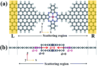 |
| | Fig. 1 The structure of the bilayer CuPc molecular device. The red, blue, black, and grey balls represent Cu, N, C, and H atoms, respectively. The molecule in the scattering region is CuPc and the electrode is a V-shaped zigzag-edged GNR electrode. (a) and (b) are the top and side view of the molecular device, respectively. | |
The spin-polarized current through the central scattering region is calculated by the Landauer–Buttiker formula as follows28
| |
 | (1) |
where
e is the electron charge,
h is Planck's constant,
Tσ (
ε,
Vb) is the electron transmission coefficient for the spin-up (↑) and spin-down (↓) electrons (σ = ↑/↓),
f(
ε![[thin space (1/6-em)]](https://www.rsc.org/images/entities/char_2009.gif)
−
μL/R) is the Fermi distribution function, and
μL and
μR represent the electrochemical potentials of the left and right electrode, respectively.
Vb is the bias voltage and
Iσ is the total charge current. For every spin state,
Tσ (
ε,
V) is given by
17,28| | |
Tσ(ε, Vb) = Tr[ΓL(ε, Vb)GR(ε)ΓR(ε, Vb)GA(ε)]
| (2) |
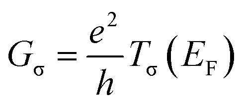
The spin-polarized conductance at zero bias is given by the Landauer–Buttiker formula28 and is derived from the current with respect to the voltage,29 as follows
| |
 | (3) |
where
EF is the Fermi level. The spin-polarized conductance unit is
G0 =
e2/
h. For each spin state,
Tσ (
EF) is given by
17| | |
Tσ(EF) = Tr[ΓLGRΓRGA]σσ
| (4) |
where
ΓL and
ΓR represent the contact broadening functions associated with the left and right electrode, and
GR and
GA stand for the retarded and advanced Green's functions of the central region, respectively.
At zero bias, SFE is defined as
| |
 | (5) |
where
T↑(
EF) and
T↓(
EF) stand for the transmission coefficient of the spin-up (SU) and spin-down (SD) states at the Fermi level, respectively.
Considering the spin direction of the lead, there is a giant magnetoresistance (MR) effect, and the MR ratios for the device for PC and APC are defined by the following two formulae20
| |
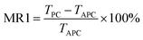 | (6) |
| |
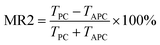 | (7) |
where
TPC =
TPC(
EF)
↑ +
TPC(
EF)
↓, and
TAPC =
TAPC(
EF)
↑ +
TAPC(
EF)
↓.
The spin-filter efficiency (SFE) with different bias voltages is defined as
| |
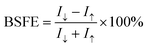 | (8) |
where
Iσ (σ = ↑, ↓, spin up: ↑; spin down: ↓) is the spin-resolved current.
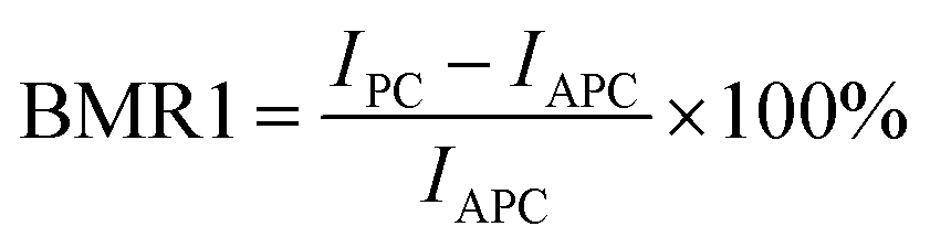
The magnetoresistance ratios at different bias voltages are defined by the following two formulae17,20
| |
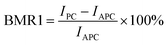 | (9) |
| |
 | (10) |
where
IPC and
IAPC are the total currents in the PC and the APC, respectively.
At zero bias, the charge and spin Seebeck coefficient are defined as SC = (S↑ + S↓)/2 and SS = (S↑ − S↓)/2, where S↑ and S↓ are the spin-up and spin-down Seebeck coefficients, respectively.30
3. Results and discussion
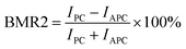
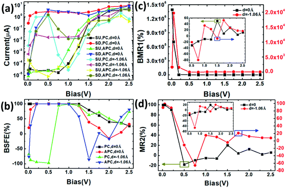
Fig. 2(a) and (b) show the SU and SD conductance versus the distance in an oscillating manner; when the distance is negative, the SU and SD conductance first increase, then decrease and then increase; the SU conductance increases and SD conductance decreases with the distance when the distance is positive in the PC. The SD conductance in the PC is larger than the one in the APC. When the distance is in the special range about −1.194 Å to −1.109 Å, the SU G is larger than the SD G (Fig. 2(c)), and when the distance is something else, the SD G is greater than the SU G. The SD and total conductance (the sum of the SU and SD conductance) reach their maximum when the distance is zero for the PC. The SU and SD conductance versus the distance in an oscillating manner are shown in Fig. 2(a) and (d).
 |
| | Fig. 2 At zero bias, (a and b) the SU and SD conductance G in the PC and APC and the detail in the range of −1.215 to −1.079 Å at the Fermi level of the CuPc molecular device versus the distance with logarithmic ordinate; (c) the SU and SD G in the PC and APC versus the distance with linear ordinate; (d) the SU and SD G in the APC versus the distance with linear ordinate. | |
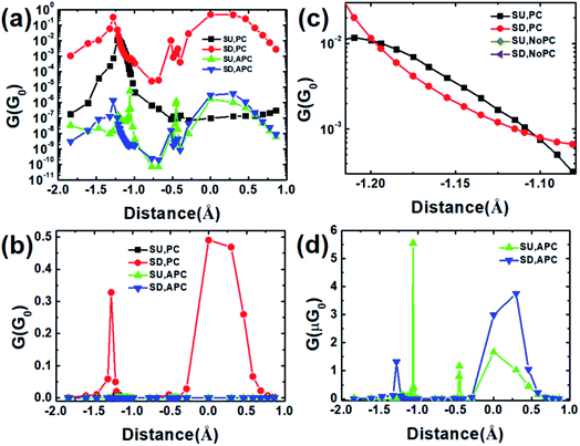
Fig. 3(a) demonstrates the transmission at the Fermi level of the CuPc molecular device versus the distance, which is exactly the same as the change rule of the conductance. According to eqn (5), there are negative SFEs, as shown in Fig. 3(b), when the SU transmission is larger than the SD transmission in the PC and APC, and the maximum and minimum SFEs are about −26.03175% and 99.99996% for the PC, and −99.93448% and 97.91% for the APC. At zero bias, the SFE also exhibits oscillation. Fig. 3(c) and (d) show the MR ratio versus the distance in an oscillating manner, and the maximum MR1 and MR2 are 5.21 × 10⁷% and 99.9996%, respectively. The SD G, total G and SFE of the bilayer CuPc molecular device for the PC are the greatest when the distance is zero, and the SD and total conductance for the APC are smaller than the ones for the PC. In other words, the electrical and spin properties of the bilayer CuPc molecular device are optimal with d = 0 Å. To understand the underlying physical mechanism, we calculated the transmission spectrum, spin polarized projected (projected onto orbitals and considering the angular momentum quantum number) density of states and the scattering states, as shown in Fig. 4 and Fig. 5.
 |
| | Fig. 3 (a) The spin-polarized transmission, (b) SFE and (c and d) MR ratio of the CuPc molecular device versus the distance. | |
 |
| | Fig. 4 The transmission and scattering states of the CuPc molecular device in the PC with d = 0 Å (d0) (a–e) and d ≈ −1.16584 Å (d1) (f–j). | |
 |
| | Fig. 5 The transmission spectrum and the spin polarized projected (projected onto orbitals and considering the angular momentum quantum number) density of states (PDOS) of the CuPc molecular device in the PC and APC with Vb = 0 V and d = 0 Å. | |
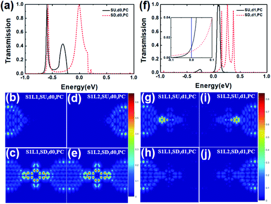
Fig. 4 demonstrates the transmission and scattering states of the CuPc molecular device in the PC with d = 0 Å (a–e) and d ≈ −1.16584 Å (f–j). For the bilayer CuPc molecular device at zero bias, the transmission at the Fermi level in the SU channel is smaller than the one in the SD channel (a) and the scattering states in the SD channel are stronger than the one in the SU channel (b–e) with d = 0 Å (SFE ≈ 99.99996%). However, there is a diametrically opposite law of change for the transmission (f) and scattering states (g-j) of the device with d ≈ −1.16584 Å (SFE ≈ −26.03175%).
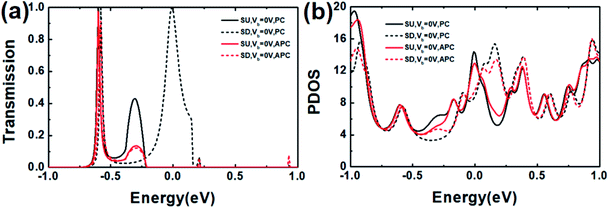
Fig. 5 shows the transmission spectrum and the spin polarized projected (projected onto orbitals and considering the angular momentum quantum number) density of states (PDOS) of the CuPc molecular device in the PC and APC with Vb = 0 V and d = 0 Å. The transmission spectrum for the PC is generally larger than the one for the APC. At the Fermi level, the SD transmission in the PC is clearly higher than the SU transmission and the transmission in the APC. As a whole, the PDOS in the PC is greater than the one in the APC.
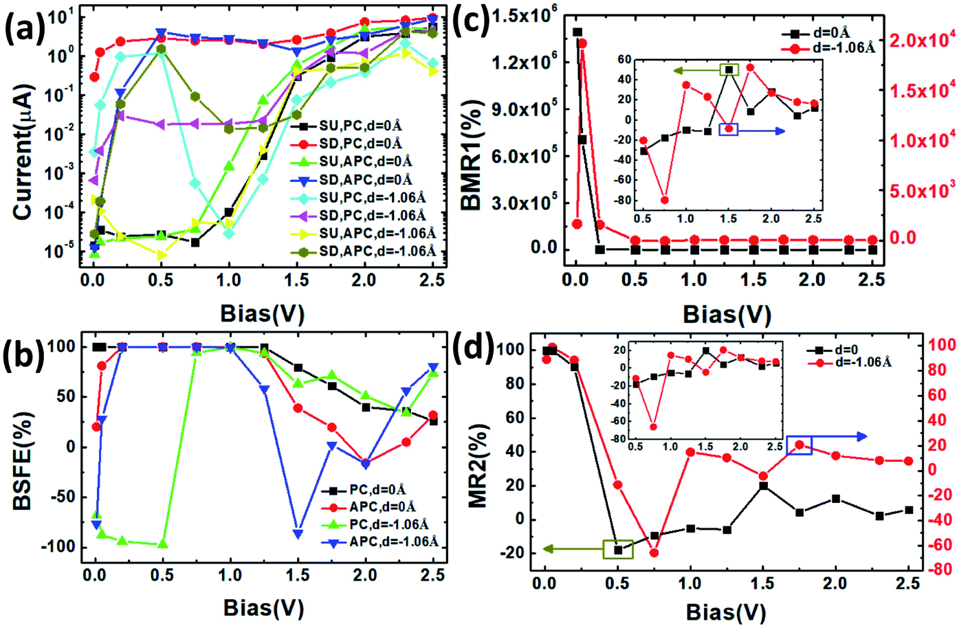
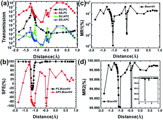
The above results drove us to investigate the effect of bias voltage on the spin filtering efficiency. Fig. 6 shows the influence of bias voltage on the electrical properties of the bilayer CuPc molecular device with the distances d = 0 Å and d = −1.06 Å for the PC and APC. There is an increasing trend for the SU and SD currents when the bias increases and the bias is larger than certain values. The SD current in the PC and APC for d = 0 Å and the SU current in the PC and SD current in APC for d = −1.06 Å show a NDR effect with an onset bias of about 0.5 V. The SU current for d = 0 Å and SD current for d = −1.06 Å show a NDR effect with an onset bias of about 0.05 V and 0.2 V, respectively. The bias-dependent spin filtering efficiency (BSFE) first increases and then decreases with the PC, and first increases, then decreases and then increases with the APC with increasing considered bias voltage when d = 0 Å and the BSFE for d = −1.06 Å oscillates with increasing bias, as shown in Fig. 6(b). The largest BSFEs for d = 0 Å and d = −1.06 Å in the PC are about 99.9986% and 99.69%, and are about 99.9988% and 99.999% in the APC, respectively. The largest reversal BSFEs for d = −1.06 Å are about −97.08% in the PC and −85.75% in the APC. For the PC and APC, there is a giant magnetoresistance effect, and the bias-dependent magnetoresistance ratios BMR1 and BMR2 change with increasing considered bias voltage in an oscillating manner when d = 0 Å and d = −1.06 Å, as shown in Fig. 6(c) and (d). The highest MR1 values are about 1.39 × 10⁶% and 1.97 × 10⁴% for d = 0 Å and d = −1.06 Å, respectively. As shown in eqn (9) and (10), the SFE and MR are determined by the SU and SD currents (Fig. 6(a)).
 |
| | Fig. 6 (a) The spin-polarized current, (b) SFE, and (c and d) MR ratio of the CuPc molecular device versus the bias voltage. | |
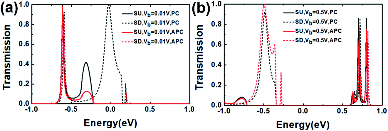
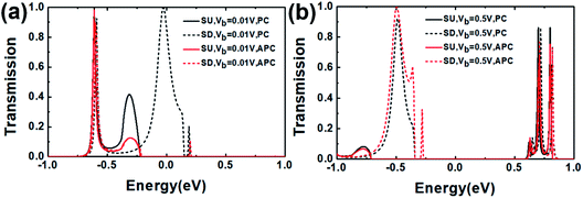
Fig. 7 shows the transmission in the SU and SD channel of the CuPc molecular device for the PC and APC with a distance of 0 Å at Vb = 0.01 V and Vb = 0.5 V.
 |
| | Fig. 7 The transmission spectrum of the CuPc molecular device in the PC and APC with Vb = 0.01 V and Vb = 0.5 V. | |
The SU and SD transmission for the PC at Vb = 0.01 V are greater than the ones for the APC (Fig. 7(a) and (b)). At Vb = 0.5 V, there is a little difference in the SU transmission in the PC and APC, and the SD transmission in the PC is lower than the one in the APC, as shown in Fig. 7(a) and (b), respectively. The change values of the SU and SD transmission at Vb = 0.01 V and Vb = 0.5 V correspond to the change of the spin-polarized current.
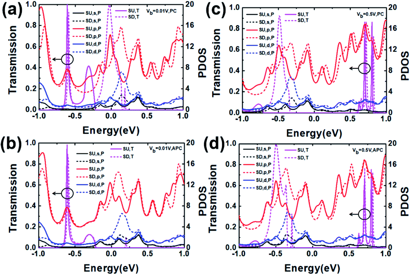
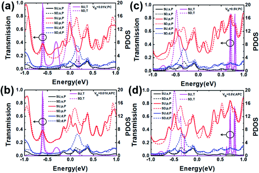
Fig. 8 shows the transmission (T) and PDOS (P) of the s, p, and d orbitals in the SU and SD channels of the CuPc molecular device for the PC and APC with a distance of 0 Å at Vb = 0.01 V and Vb = 0.5 V, which correspond to the changing rule of the spin-polarized current at bias = 0.01 V and 0.5 V.
 |
| | Fig. 8 The transmission spectrum and the spin polarized projected (projected onto orbitals and considering the angular momentum quantum number) density of states (PDOS) of the CuPc molecular devices in the PC and APC with Vb = 0.01 V in (a) and (b), and in the PC and APC Vb = 0.5 V in (c and d). | |
At bias = 0.01 V, as shown in Fig. 8(a), there are two main transmission peaks from −1 eV to 1 eV: about −0.59 eV and −0.025 eV for SD, and about −0.61 eV and −0.31 eV for SU for the PC. There is one main transmission peak for the SU and SD channel (Fig. 8(b)) at about −0.61 eV and −0.59 eV, respectively. At bias = 0.5 V, as shown in Fig. 8(c) and (d), there are two main transmission peaks of about 0.7 eV and 0.8 eV for the SU channel and three main transmission peaks of about −0.49 eV, 0.71 eV and 0.81 eV for the SD channel for the PC. For APC, there are two main transmission peaks of about 0.7 eV and 0.8 eV for the SU channel and four main transmission peaks of −0.49 eV, −0.36 eV, 0.71 eV and 0.82 eV for the SD channel (Fig. 8(d)). The origin of the transmission peaks could be figured out by projected density of states (PDOS);12 therefore, we demonstrated the PDOS of the s, p, d orbitals in the SU and SD channels of the CuPc molecular device with the PC and APC (Fig. 8). As shown in Fig. 8(a–d), the transmission is mainly controlled by the PDOS of the p orbital. The transmission peaks essentially coincide with the corresponding PDOS peaks, and most other PDOS peaks have no distribution to the transmission peaks.
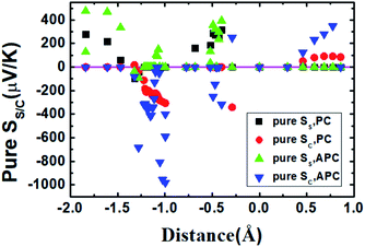
Fig. 9 shows the pure spin Seebeck coefficient (SC = 0) and charge Seebeck coefficient (SS = 0) of the CuPc molecular device in the PC and APC versus the distance. It can be seen that when the distance is greater than about 0.5 Å, there is only the pure charge Seebeck coefficient in the PC and APC, that is, there is a pure charge flow at the corresponding temperature difference. As the distance increases, the pure charge Seebeck coefficient first increases and then decreases in the PC, while the pure charge Seebeck coefficient in APC increases, that is, the corresponding pure charge flow increases. However, when the distance is about 0.859 Å, the pure SS and SC are zero, that is, there are no pure SS and SC at the corresponding temperature. When the distance is negative, in different regions, there are pure spin Seebeck coefficients and pure charge Seebeck coefficients for the PC and APC, respectively, that is, there are pure spin current and pure charge current. When the distance is around −0.5 Å, there is a positive pure spin Seebeck coefficient for the PC and APC, and there is a negative pure charge Seebeck coefficient for the APC. When the distance is near 1 Å, there is a large negative pure charge Seebeck coefficient; when the distance is less than about −1.46 Å, there is a positive pure spin Seebeck coefficient for the PC and APC, and it increases with decreasing distance, that is, there is a pure spin current increasing with decreasing distance. As shown in Fig. 10(b) and (d), when the distances are about −0.9958 Å (d2) and −1.8388 Å (d3), there are three pure SC and two pure SS at different temperatures in the APC, respectively, which means that there are three and two different temperature differences to produce pure charge current and pure spin current, respectively. Fig. 10(a) shows that the SU and SD Seebeck coefficients first decrease and then increase with the temperature; the SD Seebeck coefficient first decreases and then increases with the temperature; however, the SU Seebeck coefficient first increases, then decreases, then increases and then decreases with temperature.
 |
| | Fig. 9 The pure spin Seebeck coefficient and charge Seebeck coefficient of the CuPc molecular device in the PC and APC versus the distance. | |
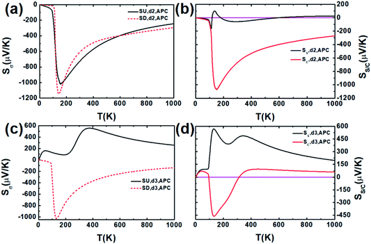 |
| | Fig. 10 The spin-dependent Seebeck coefficient Sσ, the spin Seebeck coefficient SS and the charge Seebeck coefficient SC of the CuPc molecular device in the APC versus temperature for distances of about −0.9958 Å (d2) in (a) and (b), and for distances of about −1.8388 Å (d3) in (c) and (d). | |
4. Conclusions
In conclusion, we have investigated the spin-dependent conductance, current, SFE and MR ratio of a bilayer CuPc molecular device with different buffer layer-molecule distances using DFT-NEGF. The results show that the greatest spin filter efficiency of the bilayer CuPc molecular device at zero bias exceeds 99.99996% in the parallel spin configuration and 97.91% in the anti-parallel spin configuration. Particularly, there are reserved SFEs for the PC and APC when the distances are certain values, and the reserved SFEs exceed −26.03175% and −99.93448%, respectively. For the PC and APC, there is a giant magnetoresistance effect, and the MR ratio exceeds 5.21 × 10⁷% (99.9996%). Moreover, the MR is reserved when the bias voltage is at certain values. With an applied bias, a negative differential resistance effect was observed for the distance at certain values, such as d = 0 and −1.06 Å. When the distances are certain values, there are pure spin Seebeck coefficients and pure charge Seebeck coefficients at certain temperatures, which means that the corresponding temperature differences could produce pure spin current and pure charge current. Our results provide a promising approach for designing high-performance spintronic and spin thermoelectric molecular devices.
Conflicts of interest
There are no conflicts to declare.
Acknowledgements
This work was supported by the National Key Research and Development Program of China under Grant No. 2021YFA1200502, the General Program of National Natural Science Foundation of China under Grant No. 12174423 and 61774168.
References
- S. A. Wolf, D. D. Awschalom, R. A. Buhrman, J. A. Daughton, S. von Molnár, M. L. Roukes, A. Y. Chtchelkanova and D. M. Treger, Science, 2001, 294, 1488 CrossRef CAS PubMed.
- S. Lakshmi, S. Roche and G. Cuniberti, Phys. Rev. B, 2009, 80, 193404 CrossRef.
- J. Huang, W. Y. Wang, Q. X. Li and J. L. Yang, J. Chem. Phys., 2014, 140, 164703 CrossRef PubMed.
- H. Hao, X. H. Zheng, Z. X. Dai and Z. Zeng, Appl. Phys. Lett., 2010, 96, 192112 CrossRef.
- S. Schmaus, A. Bagrets, Y. Nahas, T. K. Yamada, A. Bork, M. Bowen, E. Beaurepaire, F. Evers and W. Wulfhekel, Nat. Nanotechnol., 2011, 6, 185–189 CrossRef CAS PubMed.
- A. R. Rocha, V. M. Garcia-Suárez, S. W. Bailey, C. J. Lambert, J. Ferrer and S. Sanvito, Nat. Mater., 2005, 4, 335 CrossRef CAS PubMed.
- N. Atodiresei, J. Brede, P. Lazic, V. Caciuc, G. Hoffmann, R. Wiesendanger and S. Blugel, Phys. Rev. Lett., 2010, 105, 066601 CrossRef PubMed.
- H. Wan, B. Zhou, X. Chen, C. Q. Sun and G. Zhou, J. Phys. Chem. C, 2012, 116, 2570 CrossRef CAS.
- X. Q. Deng, Z. H. Zhang, G. P. Tang, Z. Q. Fang, L. Sun and C. X. Li, Org. Electron., 2016, 35, 1 CrossRef CAS.
- T. Tada, S. Hamayama, M. Kondo and K. Yoshizawa, J. Phys. Chem. B, 2005, 109, 12443 CrossRef CAS PubMed.
- Y. F. Wang, J. Kroger, R. Berndt and W. A. Hofer, J. Am. Chem. Soc., 2009, 131, 3639 CrossRef CAS PubMed.
- C. C. Zhao, S. H. Tan, X. F. Peng, X. J. Wang and M. Q. Long, Org. Electron., 2017, 43, 47–54 CrossRef CAS.
- C. Arrigo, F. Andrea and N. M. Buongiorno, Nanotech, 2007, 18, 15464 Search PubMed.
- J. Zeng and K. Q. Chen, J. Mater. Chem. C, 2013, 1, 4014 RSC.
- Y. D. He, H. L. Dong, T. Li, C. L. Wang, W. Shao, Y. J. Zhang, L. Jiang and W. P. Hu, Appl. Phys. Lett., 2010, 97, 133301 CrossRef.
- J. Huang, K. Xu, S. Lei, H. Su and S. Yang, J. Chem. Phys., 2012, 136, 064707 CrossRef PubMed.
- L. L. Tao and J. Wang, Nanoscale, 2017, 9, 12684–12689 RSC.
- D. Waldron, P. Haney, B. Larade, A. MacDonald and H. Guo, Phys. Rev. Lett., 2006, 96, 166804 CrossRef PubMed.
- B. Wang, J. W. Li, Y. J. Yu, Y. D. Wei, J. Wang and H. Guo, Nanoscale, 2016, 8, 3432–3438 RSC.
- X. X. Han, J. J. Yang, P. P. Yuan and B. A. Bian, Eur. Phys. J. B, 2019, 92, 32 CrossRef.
- X. X. Fu, F. Wei, Y. Niu and C. K. Wang, Phys. E, 2021, 131, 114737 CrossRef CAS.
- J. H. Liu, K. Luo, K. L. Huang, B. Sun, S. L. Zhang and Z. H. Wu, Nanoscale Adv., 2021, 3, 3497–3501 RSC.
- Z. H. Wu, L. Z. Lin, W. Yang, D. Zhang, C. Shen, W. Lou, H. Yin and K. Chang, RSC Adv., 2017, 7, 30963–30969 RSC.
- P. Hohenberg and W. Kohn, Phys. Rev., 1964, 136, 864–871 CrossRef.
- W. Kohn and L. J. Sham, Phys. Rev., 1965, 140, 1133–1138 CrossRef.
- J. Taylor, H. Guo and J. Wang, Phys. Rev. B, 2001, 63, 245407 CrossRef.
- L. L. Cui, B. C. Yang, X. M. Li, J. He and M. Q. Long, Int. J. Mod. Phys. B, 2014, 28, 1450019 CrossRef.
- M. Buttiker, Y. Imry, R. Landauer and S. Pinhas, Phys. Rev. B, 1985, 31, 6207–6215 CrossRef PubMed.
- N. A. Bruque, M. K. Ashraf, G. J. O. Beran, T. R. Helander and R. K. Lake, Phys. Rev. B, 2009, 80, 155455 CrossRef.
- M. X. Zhai, X. F. Wang, P. Vasilopoulos, Y. S. Liu, Y. J. Dong, L. P. Zhou, Y. J. Jiang and W. L. You, Nanoscale, 2014, 6, 11121–11129 RSC.
Footnote |
| † These authors contributed equally. |
|
| This journal is © The Royal Society of Chemistry 2022 |
Click here to see how this site uses Cookies. View our privacy policy here. 
 Open Access Article
 This Open Access Article is licensed under a Creative Commons Attribution-Non Commercial 3.0 Unported Licence
 ab,
Kun Luo†ab,
Hudong Changab,
Bing Sunab,
Shengli Zhang
ab,
Kun Luo†ab,
Hudong Changab,
Bing Sunab,
Shengli Zhang