
 Open Access Article
 This Open Access Article is licensed under a
 Creative Commons Attribution 3.0 Unported Licence
High performance and gate-controlled GeSe/HfS2 negative differential resistance device†
Amir Muhammad Afzal *a,
Muhammad Zahir Iqbalb,
Muhammad Waqas Iqbala,
Thamer Alomayric,
Ghulam Dastgeerd,
Yasir Javede,
Naveed Akhter Shadf,
Rajwali Khang,
M. Munir Sajidf,
R. Neffatihi,
Tasawar Abbasa and
Qudrat Ullah Khanj
*a,
Muhammad Zahir Iqbalb,
Muhammad Waqas Iqbala,
Thamer Alomayric,
Ghulam Dastgeerd,
Yasir Javede,
Naveed Akhter Shadf,
Rajwali Khang,
M. Munir Sajidf,
R. Neffatihi,
Tasawar Abbasa and
Qudrat Ullah Khanj
aDepartment of Physics, Riphah International University, 13 Raiwind Road, Lahore, Pakistan. E-mail: amirafzal461@gmail.com
bNanotechnology Research Laboratory, Faculty of Engineering Sciences, GIK Institute of Engineering Sciences and Technology, Topi 23640, Khyber Pakhtunkhwa, Pakistan
cDepartment of Physics, Faculty of Applied Science, Umm-Al-Qura University, 21955, Makkah, Saudi Arabia
dDepartment of Physics & Astronomy, Graphene Research Institute–Texas Photonics Center International Research Center (GRI–TPC IRC), Sejong University, Seoul 05006, Korea
eDepartment of Physics, University of Agriculture, Faisalabad, 38000, Pakistan
fDepartment of Physics, GC University, Faisalabad, 38000, Pakistan
gDepartment of Physics, University of Lakki Marwat, Lakki Marwat, KPK, Pakistan
hDepartment of Physics, Faculty of Science, King Khalid University, P.O. Box 9004, Abha, Saudi Arabia
iLaboratoire de Physique de la Matière Condensée, Département de Physique, Faculté des Sciences de Tunis, Université Tunis El Manar, Campus Universitaire, 1060 Tunis, Tunisia
jGreater Bay Area Institute of Precision Medicine (Guangzhou), Fudan University, Nansha District, Guangzhou, Guangdong 511458, P. R. China
First published on 5th January 2022
Abstract
Transition metal dichalcogenides (TMDs) have received significant attention owing to their thickness-dependent folded current–voltage (Ids–Vds) characteristics, which offer various threshold voltage values. Owing to these astonishing characteristics, TMDs based negative differential resistance (NDR) devices are preferred for the realization of multi-valued logic applications. In this study, an innovative and ground-breaking germanium selenide/hafnium disulfide (p-GeSe/n-HfS2) TMDs van der Waals heterostructure (vdWH) NDR device is designed. An extraordinary peak-to-valley current ratio (≈5.8) was estimated at room temperature and was used to explain the tunneling and diffusion currents by using the tunneling mechanism. In addition, the p-GeSe/n-HfS2 vdWH diode was used as a ternary inverter. The TMD vdWH diode, which can exhibit different band alignments, is a step forward on the road to developing high-performance multifunctional devices in electronics.
Introduction
Graphene (Gr), formed from a single layer of carbon atoms, is considered to be a suitable material for use in field-effect transistors (FETs), photodetectors and sensors owing to its zero bandgap.1–4 The zero bandgap in Gr has inspired researchers to develop a novel family of materials that possess a suitable bandgap and have analogous features.5,6 Beyond the discovery of Gr,7 the transition metal dichalcogenides (TMDs) are considered to possess remarkable high performance electronic and optoelectronic characteristics.8 TMDs based devices are widely used in different applications, such as photovoltaics, data storage, diodes, and as chemical sensors.9–13Black phosphorus (BP) and molybdenum ditelluride (MoTe2) have been widely used in high-performance devices because of their thickness-dependent bandgap and work function, large hole charge carrier densities, and unexpected mobility. Recently, both materials have attracted extraordinary attention owing to their unique optical characteristics.14–16 On the other hand, the electronic and optical properties show deterioration because both TMDs are unstable and easily oxidized under ambient conditions.17 In contrast, GeSe, an emerging and auspicious p-type transition metal dichalcogenide (TMD), with a unique structure, is considered to be an alternate to BP. The bandgap nature of GeSe changes from indirect (1.08 eV) to direct (1.7 eV) in the bulk compared to the monolayer, respectively.18–20 It has significant application potential in FETs, chemical sensors, and photovoltaic devices.21
Other widely studied Hf-based layered TMDs, such as HfS2 and HfSe2, in which the layers are linked by van der Waals forces, have been discovered. The HfS2 has an octahedral coordinate structure with an indirect bandgap (1.1–1.2 eV) in the case of the monolayer.22 It has broad applications in electronics and optoelectronics because of its narrow bandgap, large and tunable work function, and huge mobility.23–25 It is clear from the literature that the device applications of HfS2 are quite limited. Contact resistance also plays a vital role in the performance of the devices; a genuine issue is presented when the work function is not the same as that of the TMDs materials and metal contacts.26,27 If there is contact resistance between the metal contact and the TMDs materials it is difficult to achieve a high performance in electronics and optoelectronics. By stacking the TMDs materials, a compact system is developed called the van der Waals heterostructures (vdWHs), which offers a novel platform to develop nano-devices.
The nano devices based on 2D-TMDs vdWHs have been efficiently used in FETs,28 sensors,29 data storage devices,30 photodetectors,31–34 integrated circuits,35 energy storage,36 amplifiers,37 inverters,38 spin-field effect transistors,39 water splitting,40 and diodes.38,41 Heterostructures and homojunction type devices have been designed by the doping of TMDs materials (chemically and electrostatically), and Fermi-level pinning. These techniques are not suitable for use in a high-performance device. The performance of the devices decreased with the passing of time. Secondly, the performance of the TMDs based nano devices is also controlled by controlling the Schottky barrier height (ϕB) of the metal–TMDs junction.38,42 The ϕB is considered to be a key parameter to control the performance of nano devices.
Hence, the 2D-TMDs vdWHs multifunctional devices with extraordinary performances, such as negative differential resistance (NDR) diode type devices and a high value of peak-to-valley current ratio, have yet to be realized. In this research, we fabricated advanced and unique GeSe/HfS2 vdWHs for multiple applications, such as NDR diode type devices and broadband photo-detecting. Each material (p-GeSe and n-HfS2) was characterized using different metal contacts to estimate the low resistance electrode and high mobility. The high peak-to-valley current ratio values were estimated at room temperature and explain the tunneling and diffusion currents using the tunneling mechanism. These high gate-modulated NDR characteristics, with an extraordinary peak-to-valley current, represent an outstanding potential in electronics, which are likely to be essential when developing highly efficient multi-valued logic applications.
Materials and methods
Device fabrication
Nano-flakes of the TMDs material (p-GeSe and n-HfS2) were obtained by mechanical exfoliation. The Scotch tape method was used to exfoliate the materials. The dry transfer method was used to fabricate the NDR devices. A compound microscope was used to observe and estimate the thickness of the p-GeSe flakes. After selection of the GeSe flake, a polydimethylsiloxane (PDMS) stamp was used to make the n-HfS2 flake a suitable size and it was then placed onto a p-GeSe flake with a micro-aligner stage. The electrode pattern was designed, and a thermal evaporation system was used for the metal contacts of (Pd/Au, Ni/Au, Cr/Au, and Ag/Au: 6/60 nm) and (Sc/Au, Al/Au, Ti/Au, Pt/Au: 6/60 nm) for p-GeSe and n-HfS2, respectively. For the lift-off process, acetone was used.All of the measurements (electrical) were performed in a vacuum box with a Keithley-2400 and Keithley-6485.
Results and discussion
The p-type GeSe was exfoliated and moved onto the substrate (p-Si/SiO2 = 300 nm) with the help of a micro-aligner attached to the camera of a microscope. The n-type HfS2 was transferred onto the GeSe to form the vdWHs. A schematic diagram is shown Fig. 1a. The optical image of the final device is shown in Fig. 1b. Raman spectroscopy was used for the identification of materials. Fig. 1c shows the Raman spectra of each material (GeSe and HfS2) and the heterostructure. Raman spectroscopy was used to determine the nature of the materials. Fig. 1c shows the Raman spectra of GeSe, HfS2, and GeSe/HfS2. The peaks that appear at 151.8 and 191 cm−1 in the case of GeSe match those observed in the previously published literature.19,43 In the case of n-HfS2, the Raman peaks appeared at 260 and 337 cm−1 and the Raman modes are consistent with previous reports.44,45 | ||
| Fig. 1 (a) Schematic diagram of the GeSe/HfS2 broken band gap p–n heterojunction device. (b) Optical image of the p-GeSe/n-HfS2 broken band gap p–n junction. (c) Raman spectroscopy of each flake (GeSe and HfS2) and the heterojunction (GeSe/HfS2) device, respectively. (d) Mobility of the p-GeSe and HfS2 TMDs with different electrodes. | ||
Atomic force microscopy (AFM) was used to determine the thickness of the p-GeSe and n-HfS2 flakes, and these were found to lie in the range of 16 and 28 nm, respectively. The AFM image with height profiles is shown in Fig. S1a and b (ESI†). The electrode Pd/Au and Sc/Au is used for p-GeSe and HfS2, respectively, to form the low resistance contacts. The types of charge carriers in p-GeSe and n-HfS2 were confirmed by the transfer curve at a constant Vds = 0.5 V (Fig. S2a and b†). The Vbg was swept between ±40 V and measured the output across the source to the drain.
First, we measured the p-GeSe and n-HfS2 field-effect transistors with dissimilar metal electrodes and then performed electrical measurements. To estimate the electrical performance, the charge carrier mobility (μFE) of p-GeSe and n-HfS2 was measured. The μFE of the device was extracted by using the following relationship:46
 | (1) |
In which, L and W represent the length and width of the channel respectively,  provides the slopes, and Cbg is the gate capacitance. In GeSe FET, the estimated μFE were observed to be Pd = 90.7, Ni = 74.5, Cr = 51.4, and Ag = 43.5 cm2 V−1 s−1.47 Secondly, the conceived μFE in the case of n-HfS2 with Sc, Al, Ti, and Pt were found to be 75, 61.6, 42.5, and 36 cm2 V−1 s−1 (Fig. 1d). In the case of the ohmic contacts (Pd–GeSe/Sc–HfS2), a large hole/electron mobility and lower value of the threshold voltage were obtained because of the high/low work function, respectively. The Pd/Sc metals with a high/low work function doped the GeSe/HfS2 TMDs materials and improved the charge carrier densities in the channel of the device. Furthermore, the current–voltage (Ids–Vds) characteristics were estimated using various contacts to determine the linear and non-linear behavior of the electrodes. Fig. S3† displays the Ids–Vds curves of the GeSe and HfS2 with various metal contacts. The metal contact (Pd), which has a high work function, shows a linear behavior (ohmic) with GeSe. Other metals show non-linear curves because of the difference in the work function. The linear behavior of the Ids–Vds curves validate the ohmic behavior because of the low potential barrier between the junction of the metal–TMDs. Furthermore, the Ids–Vds characteristics were also measured with different electrodes (Sc, Al, Ti, and Pt) to find the most suitable electrode for high-performance n-HfS2 devices. Primarily, the linear tendency of the Ids–Vds characteristics depends on the difference in the work function between the metal and TMDs materials and potential barrier between them. The energy band diagram of the GeSe with different metals before and after contact between the metals and the GeSe material is shown in Fig. S4.† The values of the work functions, electron affinities and bandgaps of GeSe and n-HfS2 were taken from previously reported studies.41,48–56
Temperature-dependent electrical measurements were performed to obtain the Schottky barrier height (ϕB). Then, we extracted the ϕB between the metals with TMDs by using the standard current model for thermionic emission, given as:
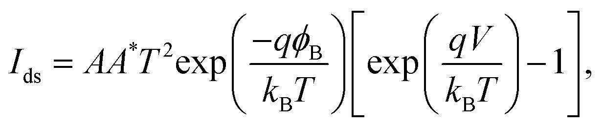 | (2) |
 plotted against
  , which is used for the estimation of the ϕB height at metal–TMD junctions. The estimated values of ϕB are 29, 45, 58, and 68 meV for Pd, Ni, Cr, and Ag, respectively. In the case of HfS2, the obtained values of ϕB are 41, 52, 60, and 78 meV for Sc, Al, Ti, and Pt, respectively. After the optimization of the most suitable electrode for the Pd–GeSe/Sc–HfS2 vdWH heterojunction device, the NDR characteristics were measured. After successfully designing the GeSe/HfS2 TMDs vdWH NDR device, the electrical measurement was performed at room temperature. Fig. 2a shows the current–voltage values (Ids–Vds) are measured at zero back gate voltages (Vbg). The device demonstrates a high value for the peak-to-valley current ratio (PVCR = 5.4) between 0.5 V and 1.1 V, which is larger than the previously reported literature values.57,58 The highest and lowest values of the current are called the peak current (Ipeak) and the valley current (Ivalley). Fig. 2b shows the gate-dependent Ids–Vds characteristics, which indicates that the peak current (Ipeak) is successfully modulated using the back gate voltage (Vbg). When the Vbg decreases, the Ipeak also decreases. When the Vbg is tuned from 40 V to −40 V, the Fermi level (Ef) of GeSe moves downward because of the accumulation of charge carriers (holes).59
 | ||
| Fig. 2 Electrical measurement of the p-GeSe/n-HfS2 NDR devices. (a) Current as a function of the bias voltage at Vbg = 0 V. (b) Change in current at different Vbg of p-GeSe/n-HfS2 NDR devices. (c) Change in the peak to the valley with back gate voltage at room temperature. (d) Change in the peak current and valley current versus the number of cycles. | ||
As a result, the energy band bending of GeSe is increased. The Ef of HfS2 is hardly tuned by Vbg because of the thick GeSe. The shifting of the energy band in the downward direction in GeSe behaves like a potential well at the interface of the heterojunction, which decreases the Ipeak. It is difficult to escape the charge carriers from the potential well because of the strong confinement of the electron carriers in the potential well. Therefore, the value of PVCR for the heterojunction was tuned to between 3.83 and 5.87 A/A using the Vbg (−40 V to 40 V) (Fig. 2c). To check the stability of the Ipeak to Ivalley, ten consecutive Ids–Vds sweeps were measured. The estimated values show stable peak- and valley-current values (Fig. 2d).60
For a graphical explanation of the NDR mechanism, a band energy diagram is shown in Fig. 3. Fig. 3a shows the band energy diagram of the GeSe/HfS2 TMDs vdWH NDR device before and after contact at a zero biased voltage. The Efof the GeSe and HfS2 are aligned after contact at the same level. A type-III bandgap (broken bandgap) was developed between the GeSe and HfS2 because the valence band of the GeSe exists above the conduction band of HfS2. The current mechanism can be explained based on the diffusion and tunneling current by using the band energy diagram. Fig. 3b shows the energy band diagram of the GeSe/HfS2 TMDs vdWH NDR device under a different bias voltage. At a negative bias voltage (Vds < 0 V), the tunneling current becomes prominent over the diffusion current. During the negative region, the charge carriers (electron) tunnel from GeSe (filled valence band states) to HfS2 (empty conduction band states), which amplifies the current. The tunneling current also becomes prominent between 0 and 0.5 V. In this region, the charge carriers (electrons) tunnel from the conduction band of HfS2 to the empty valence states of GeSe, increasing the current. The current is unceasingly enhanced in anticipation of the Fermi level of HfS2, which is aligned with the uppermost valence band energy of the GeSe. The overlapping of the filled states in HfS2 with unoccupied states in GeSe gives rise to the maximum tunneling current (Ipeak). In the range of 0.5 V < Vds < 1 V, the magnitude of the current is decreased because of the reduction in the degree of overlap between the filled and empty states. Therefore, the tunneling current is decreased as the Vbias is increased, which results from the NDR behavior in the heterojunction device. At a higher bias voltage (Vds > 0.5 V), the diffusion current predominantly contributes to the NDR behavior of the GeSe/HfS2 TMDs vdWH NDR device. In this region, the electrons are capable of diffusing from HfS2 to GeSe by attenuating the potential well, which again increases the current in the device.
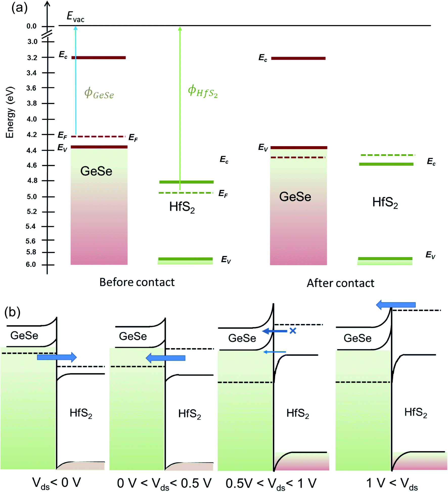 | ||
| Fig. 3 (a) Energy band diagram of the p-GeSe/n-HfS2 NDR heterojunction device before contact and after contact at zero back gate voltage. (b) Energy band diagram of the p-GeSe/n-HfS2 NDR device at different Vds. | ||
Furthermore, to check the effect of temperature, the Ids–Vds measurements were performed at different temperatures from 50–300 K (Fig. 4a). We observed that the Ipeak is improved, whereas the Ivalley declined with the falling temperature (Fig. 4b and c). The value of the peak-to-valley current was enhanced from 5.8 to 10 A/A with the temperature (Fig. 4d). The values of the peak voltage and valley voltage were shifted towards positive values. To confirm the highest values (Table S1†) of the peak and valley current, the analytic NDR device model was used. The Ids–Vds characteristics were also measured using this model and the peak-to-valley ratio was estimated. The total current (tunneling and diffusion current) is calculated by using the following equation:52
 | (3) |
 | (4) |
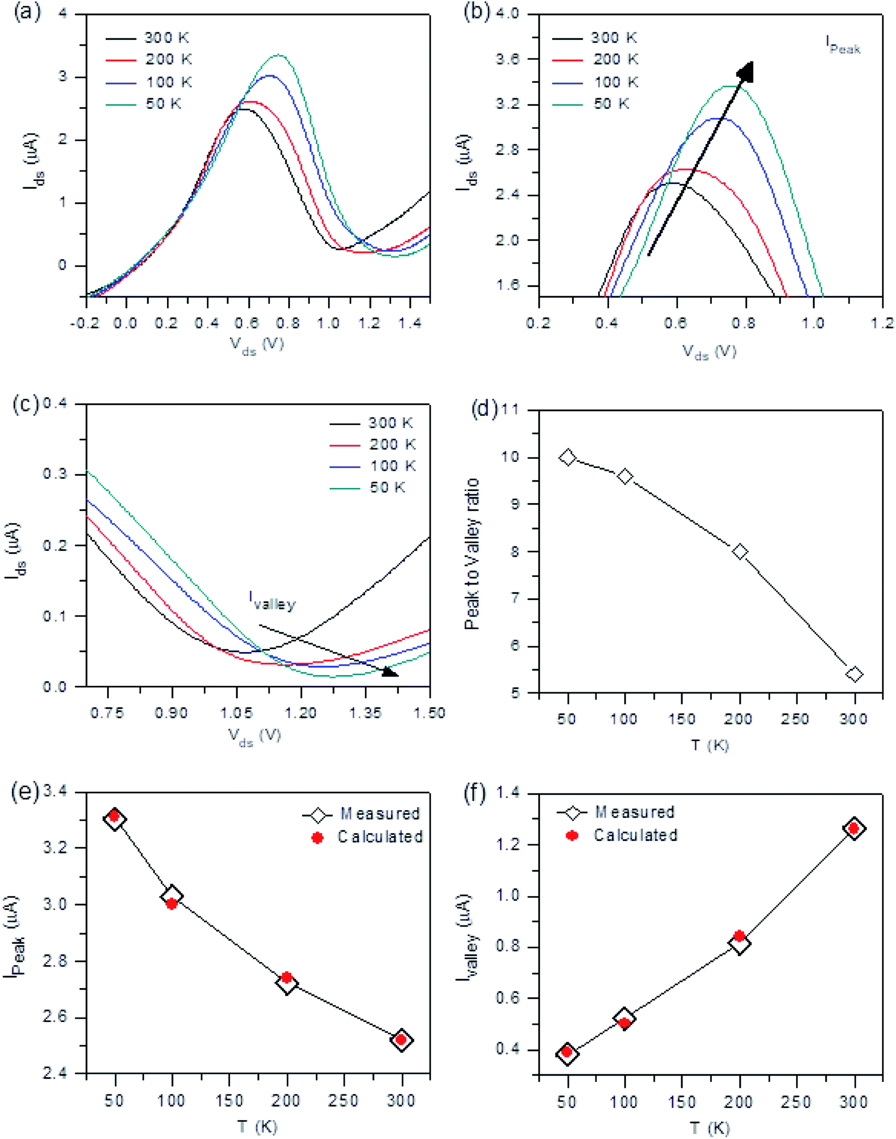 | ||
| Fig. 4 (a) Current–voltage (Ids–Vds) characteristics of the GeSe/HfS2 NDR device at different temperatures. (b) Change in the valley current with the temperature. (c) Change in the valley current with the temperature of the GeSe/HfS2 NDR devices. (d) Change in the peak to valley current with temperature of the GeSe/HfS2 NDR devices. (e) Comparison of the measured and calculated value of the peak current as a function of time. (f) Comparison of the measured and calculated value of the valley current as a function of time. | ||
In which α, Ev − GeSe, Ec − HfS2, DOSGeSe(E), DOSHfS2(E), fGeSe(E), and fHfS2(E) represents the screening factor, the highest valence band energy in GeSe, the lowest conduction band energy in HfS2, the density of states and the Fermi–Dirac distribution functions of GeSe and HfS2, respectively. Fig. 4e and f show the measured and calculated values, which demonstrate the consistency of the results. The measured value is obtained from the experimental data. The calculated value is conceived from the theoretical Ids–Vds curves estimated using the analytical model.
Basically, most of the Ipeak is primarily occupied by tunnel currents. The Ipeak looks to be allied with the density of states in the CB and VB of the HfS2 and GeSe. Both the current values (Ipeak and Ivalley) show different behaviors because the tunneling current is increased and the diffusion current is decreased as the temperature decreases. The parasitic series resistance (Rs) was also determined using the analytic model to enable accurate analysis. The Rs is the contact resistance between the contact and TMD materials. The metal–semiconductor (MS) junction resistance is enhanced at a lower temperature because of the decline in the n-type charge carriers, which leads to an enhanced depletion width at the MS junction. Therefore, a high voltage value is required to operate the NDR device at a lower temperature.61,62 We measured multiple devices of the same thickness to check the self-consistency (Fig. S6†). The effect of the thickness is also measured, as shown in Fig. S8.† In the case of a few layers, the device shows a linear behavior because of direct tunneling. Finally, an innovative ternary inverter has been designed, which is the elementary building block of multivalued logic applications. This ternary inverter is fabricated by using the GeSe/HfS2 TMDs vdWH. In most thin-film transistors (TFT), the BP was used as p-channel materials that oxidize in the ambient environment and decrease the performance of the devices.52
To overcome this critical issue, we used p-GeSe as a p-channel material. The entire resistance (R) in GeSe could be controlled by Vbg. The source and back gate electrodes were used as a supply and input voltage, respectively. The electrode on HfS2 is connected to the ground. The output voltage is measured across the middle-shared electrode. Fig. 5d shows the change in VOUT as a function of VIN at fixed VDD = 2 V from 5 to 25 V. We observed three distinct states that are mentioned as state-2, state-1, and state-0. At state 2, the output voltage is greater than 1.75 V, which appears at 4.9 V< VInput < 7.9 V. In state-1 and 0 the output voltage is around 0.85 and 0.22 V, respectively (Fig. 5d). Load line circuit analysis was performed to explain the working of the inverter. The point of intersection between the two curves indicates the point of operation of the circuit (Fig. 5c and d).
 | ||
| Fig. 5 Ternary inverter (p-GeSe/n-HfS2 NDR) device: (a) an analog circuit representation of the ternary inverter p-GeSe/n-HfS2 NDR device. (b) Output versus input characteristics of the ternary inverter p-GeSe/n-HfS2 NDR device. (c and d) Load line analysis under different bias conductions for the GeSe/HfS2 ternary inverter device. | ||
During the low voltage range, the load resistor offers a path with a small resistance between the source and drain. In this state, the input voltage is higher than the threshold voltage and a high value of the output voltage is obtained, which is almost equal to the VDD. When a high voltage is applied at the input terminal, the GeSe TFT is turned off and the resistance decreases between the output terminal and the ground. At an intermediate voltage, the device works as an NDR device. The ternary device based on GeSe/HfS2 TMDs provides an opportunity to develop multi-valued logic applications.
Conclusion
In this work, we designed a novel and innovative p-GeSe/n-HfS2 TMDs vdWH diode type NDR device. An astonishing peak-to-valley current ratio (≈5.8) was conceived at 300 K. The NDR device was also measured at different back-gate voltages and the NDR behavior was successfully modulated. The performance of the NDR device was also measured at different temperatures. From an application point of view, the p-GeSe/n-HfS2 vdWH) diode was used as a ternary inverter.Conflicts of interest
The authors declare no conflicts of interest.Author contributions
A. M. Afzal performed the experimental work and wrote the manuscript. M. Z. Iqbal, M. W. Iqbal, T. Alomayri, G. Dastgeer, Y. Javed, N. A. Shad, R. Khan, M. M. Sajid, R. Neffati, T. Abbas, and Q. U. Khan helped with the experimental work.Acknowledgements
The author (R. Neffati) extends his appreciation to the Deanship of Scientific Research at King Khalid University, Saudi Arabia for funding this work through the Research Groups Program under grant number (R.G.P.2/170/42).References
- A. K. Geim and K. S. Novoselov, in Nanoscience and Technology: A Collection of Reviews from Nature Journals, World Scientific, 2010, pp. 11–19 Search PubMed.
- E. P. Randviir, D. A. Brownson and C. E. Banks, Mater. Today, 2014, 17, 426–432 CrossRef CAS.
- Y. Zhang, Y.-W. Tan, H. L. Stormer and P. Kim, Nature, 2005, 438, 201 CrossRef CAS PubMed.
- K. S. Novoselov, A. K. Geim, S. V. Morozov, D. Jiang, Y. Zhang, S. V. Dubonos, I. V. Grigorieva and A. A. Firsov, Science, 2004, 306, 666–669 CrossRef CAS PubMed.
- K. F. Mak, C. Lee, J. Hone, J. Shan and T. F. Heinz, Phys. Rev. Lett., 2010, 105, 136805 CrossRef PubMed.
- M. Chhowalla, H. S. Shin, G. Eda, L.-J. Li, K. P. Loh and H. Zhang, Nat. Chem., 2013, 5, 263 CrossRef PubMed.
- G. R. Bhimanapati, Z. Lin, V. Meunier, Y. Jung, J. Cha, S. Das, D. Xiao, Y. Son, M. S. Strano and V. R. Cooper, ACS Nano, 2015, 9, 11509–11539 CrossRef CAS PubMed.
- P. Johari and V. B. Shenoy, ACS Nano, 2012, 6, 5449–5456 CrossRef CAS PubMed.
- H. Wang, H. Feng and J. Li, Small, 2014, 10, 2165–2181 CrossRef CAS PubMed.
- Y. Zhang, B. Zheng, C. Zhu, X. Zhang, C. Tan, H. Li, B. Chen, J. Yang, J. Chen and Y. Huang, Adv. Mater., 2015, 27, 935–939 CrossRef CAS PubMed.
- K. F. Mak and J. Shan, Nat. Photonics, 2016, 10, 216 CrossRef CAS.
- B. W. Baugher, H. O. Churchill, Y. Yang and P. Jarillo-Herrero, Nat. Nanotechnol., 2014, 9, 262 CrossRef CAS PubMed.
- M.-L. Tsai, S.-H. Su, J.-K. Chang, D.-S. Tsai, C.-H. Chen, C.-I. Wu, L.-J. Li, L.-J. Chen and J.-H. He, ACS Nano, 2014, 8, 8317–8322 CrossRef CAS PubMed.
- I. G. Lezama, A. Arora, A. Ubaldini, C. Barreteau, E. Giannini, M. Potemski and A. F. Morpurgo, Nano Lett., 2015, 15, 2336–2342 CrossRef CAS PubMed.
- C. Ruppert, O. B. Aslan and T. F. Heinz, Nano Lett., 2014, 14, 6231–6236 CrossRef CAS PubMed.
- I. G. Lezama, A. Ubaldini, M. Longobardi, E. Giannini, C. Renner, A. B. Kuzmenko and A. F. Morpurgo, 2D Mater., 2014, 1, 021002 CrossRef CAS.
- J. S. Ross, P. Klement, A. M. Jones, N. J. Ghimire, J. Yan, D. Mandrus, T. Taniguchi, K. Watanabe, K. Kitamura and W. Yao, Nat. Nanotechnol., 2014, 9, 268 CrossRef CAS PubMed.
- M. Koike, E. Shikoh, Y. Ando, T. Shinjo, S. Yamada, K. Hamaya and M. Shiraishi, Appl. Phys. Express, 2013, 6(2), 023001 CrossRef.
- H. Zhao, Y. Mao, X. Mao, X. Shi, C. Xu, C. Wang, S. Zhang and D. Zhou, Adv. Funct. Mater., 2018, 28, 1704855 CrossRef.
- A. M. Afzal, M. Z. Iqbal, S. Mumtaz and I. Akhtar, J. Mater. Chem. C, 2020, 8, 4743–4753 RSC.
- S. H. Jo, H. W. Lee, J. Shim, K. Heo, M. Kim, Y. J. Song and J. H. Park, Adv. Sci., 2018, 5, 1700423 CrossRef PubMed.
- W. Zhang, Z. Huang, W. Zhang and Y. Li, Nano Res., 2014, 7, 1731–1737 CrossRef CAS.
- C. Lei, Y. Ma, X. Xu, T. Zhang, B. Huang and Y. J. T. Dai, J. Phys. Chem. C, 2019, 123, 23089–23095 CrossRef CAS.
- J. Chang, J. Appl. Phys., 2015, 117, 214502 CrossRef.
- C. Gong, H. Zhang, W. Wang, L. Colombo, R. M. Wallace and K. Cho, Appl. Phys. Lett., 2013, 103, 053513 CrossRef.
- S. McDonnell, R. Addou, C. Buie, R. M. Wallace and C. L. Hinkle, ACS Nano, 2014, 8, 2880–2888 CrossRef CAS PubMed.
- H.-Y. Chang, W. Zhu and D. Akinwande, Appl. Phys. Lett., 2014, 104, 113504 CrossRef.
- B. Radisavljevic, A. Radenovic, J. Brivio, V. Giacometti and A. Kis, Nat. Nanotechnol., 2011, 6, 147–150 CrossRef CAS PubMed.
- W. Shi, L. Huo, H. Wang, H. Zhang, J. Yang and P. Wei, Nanotechnology, 2006, 17, 2918 CrossRef CAS.
- T. Kim, D. Kang, Y. Lee, S. Hong, H. G. Shin, H. Bae, Y. Yi, K. Kim and S. Im, Adv. Funct. Mater., 2020, 30, 2004140 CrossRef CAS.
- W. Zhu, X. Wei, F. Yan, Q. Lv, C. Hu and K. Wang, J. Semicond., 2019, 40, 092001 CrossRef CAS.
- X. Wei, F. Yan, Q. Lv, W. Zhu, C. Hu, A. Patanè and K. Wang, Adv. Opt. Mater., 2019, 7, 1900190 CrossRef.
- Q. Lv, F. Yan, X. Wei and K. Wang, Adv. Opt. Mater., 2018, 6, 1700490 CrossRef.
- F. Yan, Z. Wei, X. Wei, Q. Lv, W. Zhu and K. Wang, Small Methods, 2018, 2, 1700349 CrossRef.
- B. Radisavljevic, M. B. Whitwick and A. Kis, ACS Nano, 2011, 5, 9934–9938 CrossRef CAS PubMed.
- Z. Jiang, C. Wang, G. Du, Y. Zhong and J. Jiang, J. Mater. Chem., 2012, 22, 9494–9496 RSC.
- L. Liu, N. Xu, Y. Zhang, P. Zhao, H. Chen and S. Deng, Adv. Funct. Mater., 2019, 29, 1807893 CrossRef.
- A. M. Afzal, Y. Javed, N. A. Shad, M. Z. Iqbal, G. Dastgeer, M. M. Sajid and S. Mumtaz, Nanoscale, 2020, 12, 3455–3468 RSC.
- W. Yan, O. Txoperena, R. Llopis, H. Dery, L. E. Hueso and F. Casanova, Nat. Commun., 2016, 7, 1–6 Search PubMed.
- Y. Sun, H. Cheng, S. Gao, Z. Sun, Q. Liu, Q. Liu, F. Lei, T. Yao, J. He and S. Wei, Angew. Chem., Int. Ed., 2012, 51, 8727–8731 CrossRef CAS PubMed.
- A. M. Afzal, G. Dastgeer, M. Z. Iqbal, P. Gautam and M. M. Faisal, ACS Appl. Mater. Interfaces, 2020, 12, 19625–19634 CrossRef CAS PubMed.
- D. S. Schulman, A. J. Arnold and S. Das, Chem. Soc. Rev., 2018, 47, 3037–3058 RSC.
- Y. Mao, C. Xu, J. Yuan and H. Zhao, J. Mater. Chem. A, 2019, 7, 11265–11271 RSC.
- X.-R. Nie, B.-Q. Sun, H. Zhu, M. Zhang, D.-H. Zhao, L. Chen, Q.-Q. Sun and D. W. Zhang, ACS Appl. Mater. Interfaces, 2017, 9, 26996–27003 CrossRef CAS PubMed.
- K. Xu, Y. Huang, B. Chen, Y. Xia, W. Lei, Z. Wang, Q. Wang, F. Wang, L. Yin and J. He, Small, 2016, 12, 3106–3111 CrossRef CAS PubMed.
- Y. Ke, D. Qi, C. Han, J. Liu, J. Zhu, Y. Xiang and W. Zhang, ACS Appl. Electron. Mater., 2020, 2, 920–926 CrossRef CAS.
- S. Fathipour, N. Ma, W. Hwang, V. Protasenko, S. Vishwanath, H. Xing, H. Xu, D. Jena, J. Appenzeller and A. Seabaugh, Appl. Phys. Lett., 2014, 105, 192101 CrossRef.
- T. Kanazawa, T. Amemiya, A. Ishikawa, V. Upadhyaya, K. Tsuruta, T. Tanaka and Y. Miyamoto, Sci. Rep., 2016, 6, 22277 CrossRef CAS PubMed.
- Y. Wang, J. C. Kim, R. J. Wu, J. Martinez, X. Song, J. Yang, F. Zhao, A. Mkhoyan, H. Y. Jeong and M. Chhowalla, Nature, 2019, 568, 70–74 CrossRef CAS PubMed.
- F. A. Rasmussen and K. S. Thygesen, J. Phys. Chem. C, 2015, 119, 13169–13183 CrossRef CAS.
- J. Shang, S. Zhang, X. Cheng, Z. Wei and J. Li, RSC Adv., 2017, 7, 14625–14630 RSC.
- J. Shim, S. Oh, D.-H. Kang, S.-H. Jo, M. H. Ali, W.-Y. Choi, K. Heo, J. Jeon, S. Lee, M. Kim, Y. J. Song and J.-H. Park, Nat. Commun., 2016, 7, 13413 CrossRef CAS PubMed.
- A. M. Afzal, M. Z. Iqbal, S. Mumtaz and I. Akhtar, J. Mater. Chem. C, 2020, 8, 4743–4753 RSC.
- A. M. Afzal, M. Z. Iqbal, G. Dastgeer, G. Nazir, S. Mumtaz, M. Usman and J. Eom, ACS Appl. Mater. Interfaces, 2020, 12, 39524–39532 CrossRef CAS PubMed.
- A. M. Afzal, S. Mumtaz, M. Z. Iqbal, M. W. Iqbal, A. Manzoor, G. Dastgeer, M. J. Iqbal, Y. Javed, R. Khan, N. A. Shad, M. M. Sajid and T. Zahid, J. Mater. Chem. C, 2021, 9, 7110–7118 RSC.
- G. Dastgeer, A. M. Afzal, G. Nazir and N. Sarwar, Adv. Mater. Interfaces, 2021, 8, 2100705 CrossRef CAS.
- L. Britnell, R. V. Gorbachev, A. K. Geim, L. A. Ponomarenko, A. Mishchenko, M. T. Greenaway, T. M. Fromhold, K. S. Novoselov and L. Eaves, Nat. Commun., 2013, 4, 1794 CrossRef CAS PubMed.
- A. Mishchenko, J. S. Tu, Y. Cao, R. V. Gorbachev, J. R. Wallbank, M. T. Greenaway, V. E. Morozov, S. V. Morozov, M. J. Zhu, S. L. Wong, F. Withers, C. R. Woods, Y. J. Kim, K. Watanabe, T. Taniguchi, E. E. Vdovin, O. Makarovsky, T. M. Fromhold, V. I. Fal'ko, A. K. Geim, L. Eaves and K. S. Novoselov, Nat. Nanotechnol., 2014, 9, 808–813 CrossRef CAS PubMed.
- M. P. Mikhailova, K. D. Moiseev and Y. P. Yakovlev, Semicond. Sci. Technol., 2004, 19, R109–R128 CrossRef CAS.
- M. Mikhailova, K. Moiseev and Y. P. Yakovlev, Semicond. Sci. Technol., 2004, 19, R109 CrossRef CAS.
- V. L. Rideout, Thin Solid Films, 1978, 48, 261–291 CrossRef CAS.
- P. Zhou, J. Cheng, C. F. Schaus, S. Z. Sun, K. Zheng, E. Armour, C. Hains, W. Hsin, D. R. Myers and G. A. Vawter, IEEE Photonics Technol. Lett., 1991, 3, 591–593 Search PubMed.
Footnote |
| † Electronic supplementary information (ESI) available. See DOI: 10.1039/d1ra07276e |
| This journal is © The Royal Society of Chemistry 2022 |