
 Open Access Article
 This Open Access Article is licensed under a Creative Commons Attribution-Non Commercial 3.0 Unported Licence
Prediction of intermediate band in Ti/V doped γ-In2S3†
R. Mariyal Jebastya,
Anja Olafsen Sjåstad b and
R. Vidya*a
b and
R. Vidya*a
aDepartment of Medical Physics, Anna University, Sir C. V. Raman Advanced Science Block, Sardar Patel Road, Guindy, Chennai - 600 025, India. E-mail: vidyar@annauniv.edu
bCentre for Materials Science and Nanotechnology, Department of Chemistry, University of Oslo, PO Box 1033, N-0315 Oslo, Norway
First published on 6th January 2022
Abstract
Materials with an intermediate energy band (IB) introduced in the forbidden gap are viable alternatives to tandem configurations of solar cells for increasing the photon-conversion efficiency. One of the aspiring designs proposed for the intermediate band concept is hyperdoped (Ti, V):In2S3. Being very important in copper indium gallium sulfide (CIGS) solar cells, indium thiospinel (In2S3) is known for its three different temperature as well as pressure, polymorphs. The most stable β-In2S3 was experimentally shown to have an isolated intermediate band (IB) and exhibits sub-band gap absorption due to the completely filled IB after V-doping. Though experimental observation holds a positive signature, recent DFT studies did not show a metallic intermediate band for the V dopant in the 3+ charge state. In order to clarify this, we have taken incentive from experimental XRD analysis that V-doped β-In2S3 shows peaks from disordered In vacancies (either α or γ), in addition to the ordered In vacancies expected. Hence, we have carried out state-of-the-art DFT based computations on pure and Ti, V-doped In2S3 in the γ-phase which has not been studied yet. We considered the Ti and V dopants in various charge states. Our theoretical study including hybrid functional, does in fact find the IB in V-doped γ-In2S3. However, at equilibrium the IB lies in between the Fermi level (EF) and conduction band minimum (CBM).
1 Introduction
The imposing concept of an intermediate band gap (IB) was proposed by Luque and Martí1 in 1997, as one of the methodologies to overcome the Shockley and Queisser (SQ) limit of efficiency of solar cells. Historically, the tandem cell with three-layers has been proposed for a high efficiency of about 49%.2 However, a recently demonstrated 2D BAs/InTe tandem cell configuration reaches an experimental high photo conversion efficiency (PCE) of 30.2%.4 Furthermore, the recently reported bulk perovskites/In2S3 based tandem cell reaches a maximum PCE of 18.83%.5 Intermediate band gap solar cells (IBSCs) can potentially reach quantum efficiency of no more than 50% since the tandem cell requires two photons to emit one electron.3 However, either a band gap or sub-band gap photon is enough to drop down an electron in the case of an ideal intermediate band gap semiconductor. The expected quantum efficiency of the IBSC model is 63.1% with the radiative bands.Until now, the search for IB materials has been conducted mainly within the traditional semiconductors.1–3 The IB feature has been identified in a few wide bandgap materials with specific dopants, as reported in selected theoretical and experimental studies.6,7 Among the numerous theoretically proposed materials, special focus on wide band gap semiconductors with transition metal doping has received profound interest because of its metallic intermediate band.8–16 In this series, indium thiospinel has been a recurring material for photo-voltaic cells operating with an intermediate band.17–19 The interest over this material is stimulated due to its exotic surface chemistry in photocatalytic, photo-electrocatalytic applications,20–22 and optoelectronic devices like thin film solar cells, battery materials, as well as in the photochemical cells because of its cyclic-ability, which explains the success of In2S3.23–27
Being a promising candidate for CIGS solar cells, indium thiospinel (In2S3) allows three different temperature modifications in addition to a pressure transition.28–32 α-In2S3 is a low temperature polymorph, which takes a cubic-defect spinel structure of space group Fd![[3 with combining macron]](https://www.rsc.org/images/entities/char_0033_0304.gif) m with 1/3rd of tetrahedral indium sites remaining vacant.33 Further, the vacancy is randomly distributed and the structure can be stabilized up to 400 K. The β-In2S3 crystallizes at room temperature in the defect spinel structure with 1/4 of tetrahedral hole (Td) vacancies.34 However, the vacancies are arranged in a 41 screw axis along the c-axis. This forms tetrahedral geometry of three cubes stacked along the c-axis. At 700 K temperature, the ordered spinel is transformed into disordered cubic-spinel (α-In2S3) and with excess In content, it can be stabilized at room temperature. Hahn and Klinger suggested that the ordering of the ‘In’ atom is the main difference between the α and β phases.35
m with 1/3rd of tetrahedral indium sites remaining vacant.33 Further, the vacancy is randomly distributed and the structure can be stabilized up to 400 K. The β-In2S3 crystallizes at room temperature in the defect spinel structure with 1/4 of tetrahedral hole (Td) vacancies.34 However, the vacancies are arranged in a 41 screw axis along the c-axis. This forms tetrahedral geometry of three cubes stacked along the c-axis. At 700 K temperature, the ordered spinel is transformed into disordered cubic-spinel (α-In2S3) and with excess In content, it can be stabilized at room temperature. Hahn and Klinger suggested that the ordering of the ‘In’ atom is the main difference between the α and β phases.35
Further increases in temperature lead to complete re-arrangement of atoms resulting in a new γ-In2S3, which is stable in the trigonal phase up to the melting point.36 The γ-In2S3 is of reconstructive type and can be quenched at room temperature with substituted impurities.33 The high pressure polymorph (ε-In2S3) is a special case of a trigonal γ-In2S3 with corundum structure with hexagonal close packing.37 An unobtrusive change in physico-chemical properties will result based on the vacancy and ordered/disordered pattern of the In arrangement.38 However, the role of vacancy ordering has not received much attention from the research community so far.
The room temperature β-In2S3 has received more attention compared to other phases, while few physical properties of the other phases are predicted with the aid of theoretical calculations.25,39,40 Nevertheless, the theoretical formation energy of the various phases has not been studied yet. Even though the β and γ phases were shown to have the same ground state energy using the full potential linearized augmented planewave (FP-LAPW) method,39 only the β-In2S3 has been focused on with no further analysis on properties of γ-In2S3.
Recently, the thermodynamic and kinetic factors analyzed by Horani and Lifshitz,41 showed the structural transition of the γ to β phase. They exposed the less stable γ-phase as a room temperature polymorph in addition to the β-phase. Since the experimentally synthesized phases have not been studied yet for their bulk physical properties, Horani and Lifshitz alluded to the energy gap of nanoplatelets by correlating the electronic states of the bulk materials.
Notably for Ti:In2S3, a DFT study has shown that completely filled IB can be formed.42 Furthermore, the predicted IBSC, V-doped In2S3 (V:In2S3) also underlined the ease of structural transition from the β to γ phase. The solution processed V:β-In2S3 led to the formation of less stable V:γ-In2S3 (trigonal).43 But the doped sample is well crystallized having a quite similar band gap to that of β-In2S3. Notably, the electron paramagnetic resonance (EPR) signal at g ≈ 1.98 indicates the formation of a superimposed hyper-fine structure. Also, the coexistence of α and β phases has been observed, and both are identified with IB formation by hyperdoping of vanadium since they have a spinel structure.44 Due to the presence of doped impurities, a small transition pressure is enough to destabilize the β-phase. Upon increasing the dopant concentration the less stable γ-phase becomes stable.45–47
A recent study by Ghorbani et al.,48 using the HSE functional has included the V-impurity in different charge states. They showed that V3+ does not introduce any IB, whereas the V2+ introduces an IB that is filled. Further increase in the dopant concentration was shown to decrease the cell parameter. More generally, impurities are ascribed to reduce the pressure and temperature needed for phase-transition.49 Therefore it can be inferred that the dopants increase the strain in the lattice, leading to the reduction in the cell parameter. This could reduce the pressure required for β to γ phase transition, as reported in previous experimental observations.43 Moreover, the HSE calculation elicits the ineffective role of dopant from the absence of intermediate states by doping. On the contrary, the experimental studies show exaggerated absorption spectra with respect to doping. So, it is still an open question, whether the correlation effect or the structural transition plays a decisive role in the introduction of intermediate band states.
So we have attempted to give a quantitative conclusion for the phase transition based on the calculated free energy as supporting evidence for the above-said experimental phase transition. Moreover the present study explores the presence of an intermediate band by Ti/V doping In2S3. In addition, a comparative study to find the critical doping concentration, their influence in the electronic structure, and the energy barrier associated with the structural transition with respect to all polymorphs of In2S3 is underway, and will be published elsewhere.
Although a few studies are available on doping the β-In2S3, they have not considered the structural transition of doped β-In2S3. It is better to look into the impurity substituted γ-In2S3 rather than β-In2S3. Therefore we have put substantial effort into doping the trigonal (γ) phase of In2S3 with different charge states of Ti and V. Formation energy has been calculated for various charge states to check whether the defect structure is stable. We made a detailed analysis on the electronic structure to understand the nature of the IB introduced by the respective impurity. We have also introduced the HSE calculation for the hyper doped system along with spin polarization, in order to take into account the role of the correlation effect on the dispersion of IB.
2 Computational details
The Vienna Ab initio simulation package (VASP) was used for the total-energy calculations to study structural stability and to extract the equilibrium structural parameters.50,51 The projected augmented wave (PAW) method and Perdew, Burke, and Ernzerhof (PBE)52 parameterization of pseudo-potentials have been adopted to treat the core-valence electron interactions and exchange–correlation functional, respectively. A plane-wave basis set of 550 eV, and 4 × 4 × 2 k-point sampling was used for Brillouin zone integration. For suitable repetition of primitive cell a super cell of 60 atoms has been built. However, the defect–defect interaction is not effective for the hexagonal lattice since r1 = and Z1 = 12. For charged defect, the neutralizing background charge has been added. To provide accurate band gap results, hybrid-DFT was employed for the unit cell calculation incorporating 25% screened Hartree–Fock exchange (HSE06 functional).53 In order to place the IB introduced by the dopant accurately, we carried out the band-edge correction by taking the Eg from the HSE functional. For calculating the defect formation energy, dilute doping (TM0.08In1.92S3) by the supercell approach is carried out. The size of the super cell is selected in such a way that the formation energy is not affected by more than the allowed error value. Usually dilute doping leads to intermediate states, whereas hyper-doping is suggested for forming the IB. Therefore, after careful analysis of the position of intermediate states inside the Eg, the doping concentration has been increased to achieve a potential IB. To ensure superior agreement of our results with experimental findings, the spin-polarization has also been included in structural relaxation schemes, wherever required.
3 Results and discussion
3.1 Structural relaxation and defect formation energy
The crystal structures of the α and β-phase of In2S3 are given in Fig. 1. β-In2S3 is the well-known thermodynamically stable phase with ordered vacancies in the defect spinel structure (space group: I41/amd).34 γ-In2S3 takes a defect-Th3P4 type structure in the Rc space group (formula unit; Z = 6) with In3+ cation occupying 88.89% of 12(a) sites randomly and sulfur anions at the 16(c) sites, without any ordering of the vacancies.38 Indeed, the intrinsic defects have favorable bonding stability. The C3d point group symmetry of the structure results in three different equatorial bond lengths as shown in Fig. 2a.
 | ||
| Fig. 1 Crystal structures of (a) α-In2S3 and (b) β-In2S3. | ||
 | ||
| Fig. 2 Crystal structures of (a) γ-In2S3, (b) total energy vs. volume for γ-In2S3, (c) Gibbs free energy of γ-In2S3 and (d) defect formation energy of Ti:In2S3, and V:In2S3. | ||
The formation energy for the most studied β-In2S3 and the new γ-In2S3 has been calculated. The heat of formation energy of β-In2S3 is −2.74 eV f.u.−1 and that for γ-In2S3 is −2.63 eV f.u.−1. As the β-phase is lower in energy by only 0.11 eV compared to the γ phase, easy structural transition from β to γ phase is evidenced. In general, Gibbs free energy given by G = U + PV defines the total energy (U) for a particular pressure (P) at volume (V). Herein, the Gibbs free energy at zero pressure is −20.6 eV for the γ-In2S3 phase.
Fig. 2c shows the relative Gibbs free energy between the β and γ phases of In2S3 as a function of pressure. It shows that both the β and γ phases co-exist at 2 GPa indicating that the phase transition would occur at 2 GPa. However, the reported experimental transition pressure (6.6 GPa) is higher than the theoretically observed value. Further, before starting the defect calculation, the lattice parameters have been optimized in the equilibrium volume and fitted to the Birch–Murnaghan equation of state to find the lowest energy configuration (Fig. 2b). These optimized structural parameters are used to build the super cell.
Though the β-In2S3 crystal structure consists of octahedral (Od) and Td sites for the In atom, the transition metal dopants prefer to substitute those In-sites at Od positions. The transition metals Ti and V are substituted for the In atoms at the Od sites in the supercell. The energy required to form In vacancies is 2.341 eV. For the γ-In2S3, only the octahedrally coordinated In sites are available for substitution.
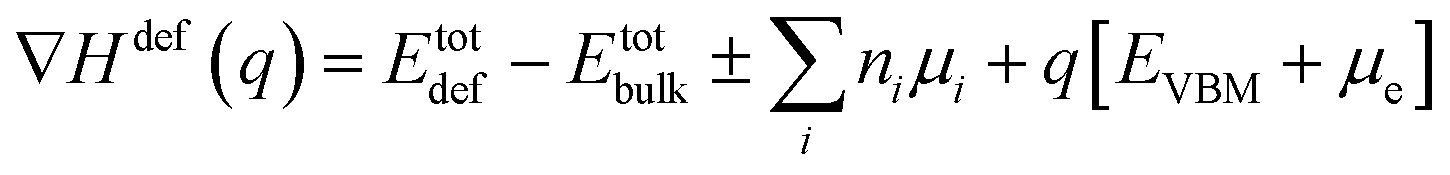
The lowest formation energy configuration is shown in Fig. 2d. The formation energy of different defects in various charge states was calculated using the formula.54
 | (1) |
Both Ti and V substituents are stable in the 1+ charge state in γ-In2S3. The 1+ charge state becomes neutralized when the EF is close to 0.25 eV above the VBM. So by manipulating the synthesis conditions it is possible to stabilize the dopants in the preferred oxidation state. When the EF is close to the VBM (p-type condition), both Ti and V have lower formation energy for donor states (i.e., 1+ charge state). On the contrary, acceptor type Ti1−In, V1−In and V2−In are stable when EF is close to the CBM (n-type condition). It can be noted that XPS studies on Fe-substituted In2S3 reveal the Fe peaks coming from Fe2+ and Fe3+ oxidation states (i.e., +1 and neutral charge states).
The EF is pinned at 0.437 eV with the co-existence of 1+ and 1− charge states of VIn. This may occur due to the reduction of V2−In into V1−In and V1+In. This aligns with the co-existence of V1−In (25%) and V0In valence states observed experimentally.43 Further, the structure is hyper-fine because of the mixed valence states. The elongation of octahedra to fit the defect inside the Od site may be the reason for reducing the valence state.
The vanadium substituent follows two defect transition paths (i) V1+In and V0In, (ii) another defect path can be followed as V1+In–V1−In–V2−In states. In the latter, the defect transition study shows that the second possibility has a direct transition of 1+ charged state to 1− state. In turn, overestimation of electron–phonon coupling takes place, thereby two electrons become attractive (negative-U). This observation indicates that the lattice experiences more vibration when transition of defect states takes place, which is reflected in the bond length. Moreover, the reduction of V2−In into V1+In is impractical since it needs a reducing agent like Li or Na etc.55 Hence the defect charge states 0/(neutral), 1− and 2− have the maximum thermodynamic probability to occur. This indicates that a charge transition occurs in the embedded dopant changes, when the Fermi energy is 0.5 eV. The triple donar impurity Ti0In and V0In, become favorable through thermal energy.
Our results lend support to the spontaneous formation of defects since all the charge states have negative formation energy. The finding here is that thermal energy can assist charged defects rather than neutral defects. Hence, the Od coordination of Ti1−In–S, and V2−In–S, seem to be quite unsuccessful. This means that defects with lower oxidation states fit better to occupy the Od symmetry sites than those with higher oxidation state. Furthermore, the transition from p-type to n-type conductivity is imminent for Ti:In2S3 and V:In2S3 near the VBM.
3.2 Electronic properties
In order to find out the favorable defects, reasonable effort has been made to analyze the complete electronic structure of the pure and doped γ-In2S3. Depending on the stabilization of the charge state of the impurities, the geometric and electronic structures become modified. First, the Eg of intrinsic γ-In2S3 has been calculated by the highly accurate HSE functional which is found to be 2.5 eV (Fig. 3a). Usually the HSE functional gives Eg close to that of experimental values; however, the experimental Eg value is not available for γ-In2S3 for comparison.41 A broad shift in the band gap from 2.15 to 2.50 eV is observed upon the structural phase change from β to γ-In2S3. This shows that a small difference in total energy of the β and γ phases induces a huge distinction within the band gap and band features. The partial density of states (pDOS) shows that the valence band maximum (VBM) is contributed to by the hybridized In-d and S-p states. The conduction band minimum (CBM) has predominant In-s states. In order to find the implications of Ti and V dopants and their charge states, on the electronic structure, the total DOS plots are given in Fig. 3b and c.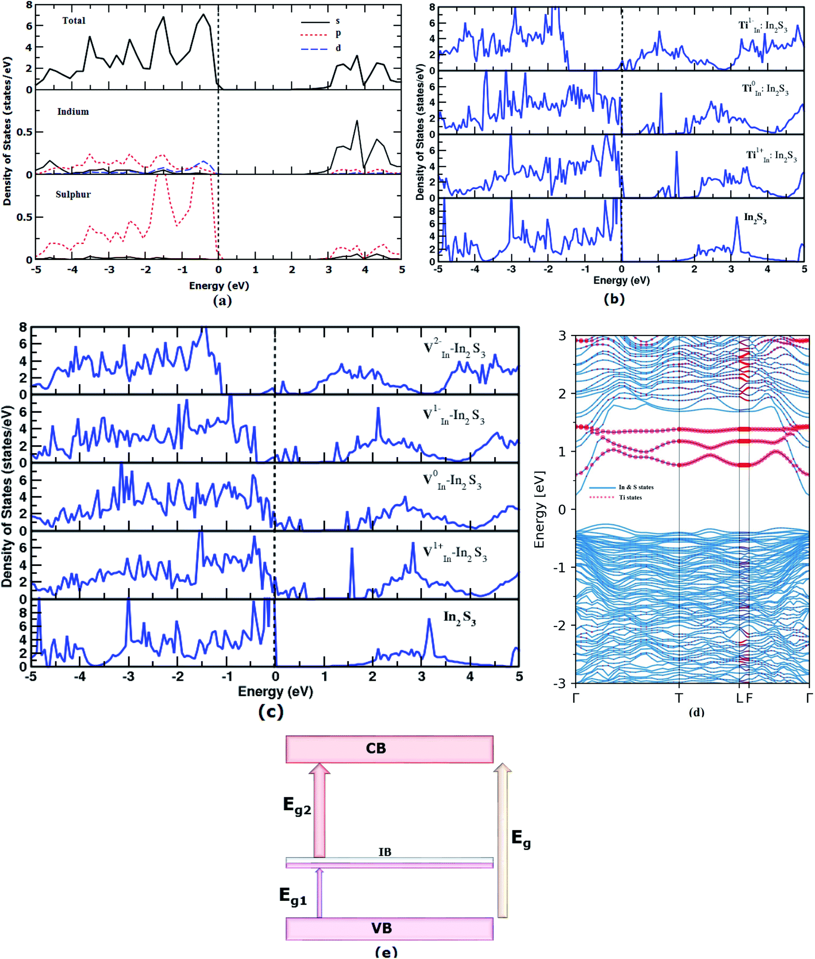 | ||
| Fig. 3 Density of states of (a) pure γ-In2S3 (b) Ti:In2S3, and (c) V:In2S3. (d) Electronic band structure of Ti0In:In2S3 and (e) illustration of the possible multi-transitions in an intermediate band semiconductor. | ||
In Fig. 3b and c, the total DOS of pristine γ-In2S3 are given in the lowest panel for comparison. The other panels illustrate the DOS plots of the substituted Ti and V atoms in different charge states. Herein, the new bands introduced between the VBM and CBM are called intermediate bands (IB) represented by total bandgap Eg, lower bandgap Eg1 and higher bandgap of Eg2. These are located in different positions within Eg based on the electronic state of the defects.
The Ti1−In does not introduce any IB whereas Ti0In and Ti1+In give rise to IB at ≈0.5 and ≈1 eV above the VBM, respectively. Hence these two later defects introduce three different band gaps (Eg) into the single semiconductor band gap. Thus, the Ti-doped γ-In2S3 can embody the IB which promotes a direct transition of electrons from the VB → IB, IB → CB and VB → CB. In a way, it helps in the effective utilization of a single incident photon to promote three excitations.
The band structure of the Ti0In defect state has been plotted along the high symmetry points (Fig. 3d). There is a significant state starting from 0.5 eV which pertains to the TM-d orbital electron. The intermediate states are highlighted in the electronic structure plot. It depicts the intermediate band of moderate width rather than discrete defect levels. The fat band analysis throws more light on the origin of the IB due to TiIn, viz., the dxy, dz2, and dx2−y2 orbitals constitute to the IB seen from 0.5 to 1.5 eV, whereas the dxz, dyz orbitals are contributing to the lower unoccupied states of the CB (given in ESI Fig. S2†).
Previous experimental studies stated that the lower energy photons are not absorbed and hence excitations from VBM to lower IB are not seen. If the IB is close to the conduction band it may enhance the possibility for the second gap transition. In this viewpoint, the ‘Ti’ substitution moves the potential IB position close to the conduction band.
In the case of V substitution at the indium site, the intermediate states fall in the EF for the V1−In and V2−In charge states. The IB seems to be a partially filled band the same as that of the VIn in the tetragonal β-In2S3. An interesting feature called the pseudo-gap is observed in the neutral state (V0In) of the defect close to the vicinity of EF (0 eV), further implicating the partial occupancy of IB. The effect of VIn on the electronic structure of β-In2S3 and γ-In2S3 is similar using the PBE functional.
Fat band analysis shows that for V0In substituted γ-In2S3, the orbitals dxy, dz2, dx2−y2 form ground state t2g states, and the dxz, dyz orbitals form the eg states (not shown here). It is worthwhile noting that the intermediate bands introduced by Ti and V substitution are well dispersed. Moreover, the dispersion of bands that were close to the VBM in undoped In2S3 increases after the Ti/V substitution. This makes the material suitable for potential photovoltaic applications.58
The position of the intermediate band solely depends on the electron count in the valence shell which is reflected in the DOS plot. Further, the intermediate band is placed in close proximity to the valence band.
3.3 Effect of hyper-doping
The optimized bond lengths of Ti, V–S and the total energy with respect to the VBM are given in the Table 1, providing information about the distortion induced by the added substituent. The In is surrounded by six sulfur atoms with octahedral co-ordination which contains the rarely observed two pairs of trigonal planar arrangements. Here, the Ti–S bond length decreases in the order Ti1−In–S > Ti0In–S > Ti1+In–S, in which Ti exists in Ti4+, Ti3+, and Ti2+ states, respectively. This implies that the Ti1+In–S defect forms the strongest covalent bonds with its S neighbours compared to the other two defects. Also, the ELF value of 0.7 clearly shows the polar covalent nature of the just mentioned bonds. This could explain the stabilization of the Ti1+In–S defect complex, in spite of less electrons being transferred from Ti to the In–S lattice.
| Compound | Charge state | Atom | Bond length (Å) | |
|---|---|---|---|---|
| (3×) | (3×) | |||
| Pure In2S3 | Neutral | In–S | 2.549 (2.513) (ref. 41) | 2.697 (2.746) |
| Ti:In2S3 | Ti1−In | In–S | 2.534 | 2.747 |
| Ti–S | 2.429 | 2.531 | ||
| Ti0In | In–S | 2.406 | 2.876 | |
| Ti–S | 2.229 | 2.574 | ||
| Ti1+In | In–S | 2.351 | 2.807 | |
| Ti–S | 2.174 | 2.505 | ||
| V:In2S3 | V2−In | In–S | 2.539 | 2.725 |
| V–S | 2.424 | 2.446 | ||
| V1−In | In–S | 2.411 | 2.756 | |
| V–S | 2.216 | 2.471 | ||
| V0In | In–S | 2.359 | 2.907 | |
| V–S | 2.092 | 2.391 | ||
| V1+In | In–S | 2.363 | 2.614 | |
| V–S | 2.295 | 2.534 | ||
However, the bond length of the V substituent site follows the order: V2−In–S > V1+In–S > V1−In–S > V0In–S, where V exists in V5+, V2+, V4+, and V3+ states, respectively. This result aligns with the experimental study,19 showing that the V substituent takes up the V3+ state. The bonding analysis shows that the lower oxidation states of V increase the stability by enhancing the covalent interaction with a shorter bond length. The reduction in bond length experienced by the V3+-dopant explains the dominant covalent bonding nature which relaxes atoms inward towards the dopant, compared to the other defect states. Further, the increase in bond length is observed for the V2+ substituent which however reduces the stability of the structure relative to the neutral case.
The electron localization function (ELF) yields visual information about the chemical bond in an easily understandable way. It depicts the 3D view of the paired electron distribution. The mapping of electron pair probability for the TM0In doped In2S3 is given in Fig. 4. The electron pair density η(r) has a proportionality relationship with the electron density (log![[thin space (1/6-em)]](https://www.rsc.org/images/entities/char_2009.gif) ρ(r)). Hence the electron density becomes maximum nearer the cation than ionic sulfur. An isosurface value of 0.7 is set to the above mentioned system to identify the difference in the electron pair distribution. The quite high value of ELF (0.7) isosurface lobes are close to the TM sites, implying the polar covalent nature of bonds. The electron localization is a kind of closed loop geometry around the Ti/V–S bonds. The sulfur atom shared by In and Ti has more ELF value and un-symmetric distribution of ELF compared to other S atoms.
ρ(r)). Hence the electron density becomes maximum nearer the cation than ionic sulfur. An isosurface value of 0.7 is set to the above mentioned system to identify the difference in the electron pair distribution. The quite high value of ELF (0.7) isosurface lobes are close to the TM sites, implying the polar covalent nature of bonds. The electron localization is a kind of closed loop geometry around the Ti/V–S bonds. The sulfur atom shared by In and Ti has more ELF value and un-symmetric distribution of ELF compared to other S atoms.
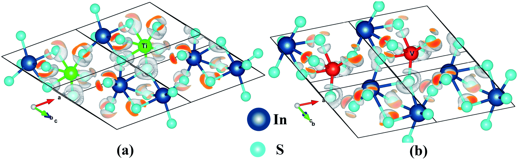 | ||
| Fig. 4 3D visualization of electron pair localization for (Rc type): (a) Ti0In:In2S3 (b) V0In:In2S3. | ||
The ELF is closer to Ti than that of V which illustrates the influence of d-electrons of the dopants on the distortion of the surrounding octahedra. Furthermore, the vanadium has much more distorted octahedral coordination for the ‘V’ substitution.
3.4 Density of states
A total density of states and the spin-resolved, atom-projected DOS are shown in Fig. 5a for the Ti0In:In2S3 (the same is given in ESI Fig. S3† for charged dopants). The heavily substituted In1.5Ti0.5S3 has an Eg of 3.5 eV. The bonding electronic states of ‘3d’ Ti, and V, clearly manifest the formation of an intermediate band. The sub-band gap Eg1 starts at 1.5 eV above EF and spreads up to 3.1 eV. This results in three different energy gap values of Eg = 3.5 eV, Eg1 = 1.2 eV and Eg2 = 0.4 eV (refer to Fig. 3e). This indicates the complete change in electronic structure due to the doping concentration beyond the saturation limit.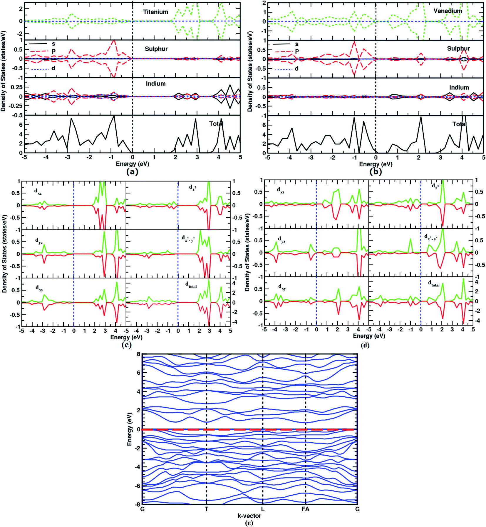 | ||
| Fig. 5 Spin-resolved density of states of (a) Ti0In:In2S3 (b) V0In:In2S3, the d-orbital projected DOS for (c) Ti in Ti0In:In2S3, (d) V in V0In:In2S3, and (e) band structure of V0In:In2S3. | ||
However, the V0In:In2S3 shows Eg similar to the undoped In2S3. The IB appearing in V0.5In1.5S3 extends from 0.6 eV above EF to 2.2 eV inside the band gap of 2.8 eV. Therefore, the entire visible light radiation can be absorbed. The optimum band position has been observed for V0.5In1.5S3 and it is similar to the experimental observation.43
In Fig. 5, the additional intermediate bands lie above EF, contrary to the previous theoretical work, where the completely occupied IB was observed. The completely filled IB can only indulge in the IB → CB transition. Then the material performance would be same as that of the un-doped semiconductor. For instance, if the band is completely filled, the e−–h+ pair generation is the same as that of an intrinsic semiconductor since the IBSC would have the IB isolated from the electrical contact. Thereby, the possibility of achieving two e−–h+ pair becomes interdependent and may be possible by the following steps: (i) the Eg2 sub-band photon should promote an e− from the IB to the CB (refer to Fig. 3e); (ii) simultaneously, the Eg1 sub-band photon would excite an e− from the VB to the IB to fill the hole created by the just-mentioned process. Therefore it can create an e−–h+ pair in addition to the e−–h+ pair introduced by the semiconductor gap (Eg). In our case, the un-filled IB can accommodate and promote an e− after the first irradiation. In fact, the present results validate the experimental observation of sub-band absorption by allowing three transitions. The overall experimental results have no significant evidence for V−2In states. So it might be reduced to lower oxidation states.
Because of the D4d symmetry of tetragonal β-In2S3, the d-band further splits into t2g and eg sub-shells, thereby causing overlapping of the lower energy states (t2g) with the VBM, and higher energy states (eg) with the CBM. This precludes the formation of IB.48 However due to the C3d symmetry of the trigonal γ-In2S3 consisting of the trigonally elongated octahedra, where the d-orbitals do not split as in the above scheme. This results in the formation of IB by Ti and V doping in γ-In2S3 as shown in Fig. 5. The corresponding d-orbital DOS of the impurity atoms (Ti and V) are given in Fig. 5c and d.
The Ti-d electron sharing the S-p orbital is ascribed to its spin alignment with the S-p orbital. A remarkable observation for this Ti dopant is the formation of an IB with Eg 1.2 eV which is the ideal band gap required for maximum absorption. It seems there is an irregular hybridization of t2g and eg states in the higher energy region. There is a strong hybridization of the p orbital of In and S along with the d states of Ti in the energy range −3 to −2.5 eV. This implies the neighboring octahedral In interaction in addition to the ligand interaction. For Ti0In, the d1-electron is distributed evenly among the t2g (dxz, dyz, and dxy) orbitals.
For a given oxidation state, the occupancy of a particular d-orbital depends upon the degree of octahedral distortion. As the S-p orbital receives electrons from In, it has completely filled states. The doped Ti-3d states are predominantly seen in the −2.5 to −3.0 eV range (Fig. 5a).
For an electrically neutral charge state for V substituents, a geometric distortion is observed with compressed trigonal structure. Here, the octahedral distortion is quite high compared to the other valence state of V substitution. Hence, the next nearest neighbouring atomic bonds and angles become very flat along the distorted direction. These ions are expected to be susceptible to angular distortions, to accommodate the impurity in different charge states. Apparently, the geometry becomes planar. This results in energetic degeneracy of dxy, dyz and dx2−y2 orbitals as the t2g ground state. Then, eg states are contributed by dxz and dz2 orbitals which are almost empty in the VB. In addition, the states are hybridized to the S-p and In-p orbitals and may provide good bonding properties of solids.
It is shown in Fig. 5e that a narrow, intermediate band is introduced as a result of hyper doping. According to our findings, the intermediate band region is completely empty. So, it can be useful for photoemission of electrons from the VB to the IB, and the IB to the CB, in addition to direct VB to CB transitions. Herein, it can assist in two step absorption by allowing photons in the energy range, 0.6 eV, 2.2 eV and 2.8 eV, respectively, to the Eg, Eg1 and Eg2. Further the IB to CB has a direct band gap, which can be tuned by varying the doping concentration. Since the IB is less dispersive, the recombination of electrons and holes through this band is not expected to be significantly high.
4 Conclusions
Based on high precision DFT calculations, the structural phase stability of pure In2S3 in β and γ variants has been studied. It is found that β-In2S3 is the most stable phase being 0.11 eV lower in energy than the γ-phase, and 2 GPa external pressure is sufficient to induce a β to γ phase transition. The experimental structure observed in V-doped In2S3 could thus result from the strain induced by the V incorporation. In order to search for the potential intermediate band, we have carried out accurate electronic structure studies using the hybrid functionals. All possible charge states of the dopant atoms were also taken into consideration. Isolated intermediate states are identified within the primary energy gap upon dilute and hyper doping of γ-In2S3, which is the new room-temperature polymorph. Ti0In and V0In defects are inferred as the influential defects with IB residing above the Fermi level (EF). It can be noted that IB can be brought down below the EF by perturbing the equilibrium either by irradiation or by filling with oxidizing agents. The transition metal induced emphatic IB in γ-In2S3 is well placed to notch up enhanced photon absorption. Either way, the conclusions do stimulate further interest for choosing the right semiconductor phase by tuning the controlled growth mechanism to have the desired valence state of the TM dopant.Conflicts of interest
There are no conflicts to declare.Acknowledgements
The author R. Mariyal Jebasty is grateful to the Centre for Research, Anna University, Chennai for offering the Anna Centenary Research Fellowship (Lr. No. CR/ACRF/2017/41) and would like to thank the ‘NaFuMa’ group, the University of Oslo, for the hospitality under the project “Theoretical and Experimental Studies on Functional Materials (TESFun)” funded by the UTFORSK program of the Centre for Internationalizing Education (SIU), Norway (UTF-2017-four-year-10089). Also, the authors thank the Research Council of Norway for the computation time in NOTUR facilities under the NN2875k project.References
- A. Luque and A. Martí, Phys. Rev. Lett., 1997, 78(26), 5014 CrossRef CAS.
- A. De Vos, J. Phys. D: Appl. Phys., 1980, 13(5), 839 CrossRef.
- A. Luque, A. Martí and C. Stanley, Nat. Photonics, 2012, 6(3), 146 CrossRef CAS.
- M. Xie, B. Cai, Z. Meng, Y. Gu, S. Zhang, X. Liu, L. Gong, X. A. Li and H. Zeng, ACS Appl. Mater. Interfaces, 2020, 12(5), 6074–6081 CrossRef CAS PubMed.
- Z. Xu, J. Wu, Y. Yang, Z. Lan and J. Lin, ACS Appl. Energy Mater., 2018, 1(8), 4050–4056 CrossRef CAS.
- L. M. Yang, P. Ravindran, P. Vajeeston and M. Tilset, J. Mater. Chem., 2012, 22(32), 16324–16335 RSC.
- T. Wang, X. Li, W. Li, L. Huang, C. Ma, Y. Cheng, J. Cui, H. Luo, G. Zhong and C. Yang, Mater. Res. Express, 2016, 3(4), 045905 CrossRef.
- P. Olsson, C. Domain and J. F. Guillemoles, Phys. Rev. Lett., 2009, 102(22), 227204 CrossRef CAS PubMed.
- P. Palacios, I. Aguilera, K. Sanchez, J. C. Conesa and P. Wahnón, Phys. Rev. Lett., 2008, 101(4), 046403 CrossRef CAS PubMed.
- P. Wahnón, P. Palacios, I. Aguilera, Y. Seminovski, J. C. Conesa José and R. Lucena. 25th European Photovoltaic Solar Energy Conference and Exhibition, 2019, pp. 203–206, DOI:10.4229/25theupvsec2010-1bo.8.5.
- P. Wahnón and C. Tablero, Phys. Rev. B: Condens. Matter Mater. Phys., 2002, 65(16), 165115 CrossRef.
- C. Tablero, Sol. Energy Mater. Sol. Cells, 2006, 90(5), 588–596 CrossRef CAS.
- Y. Seminóvski, P. Palacios and P. Wahnón, Thin Solid Films, 2011, 519(21), 7517–7521 CrossRef.
- C. Tablero, A. J. García, J. J. Fernández, P. Palacios and P. Wahnón, Comput. Mater. Sci., 2003, 27(1–2), 58–64 CrossRef CAS.
- I. Aguilera, P. Palacios and P. Wahnón, Thin Solid Films, 2008, 516(20), 7055–7059 CrossRef CAS.
- I. Aguilera, P. Palacios, K. Sánchez and P. Wahnón, Phys. Rev. B: Condens. Matter Mater. Phys., 2010, 81(7), 075206 CrossRef.
- P. Wahnón, J. C. Conesa, P. Palacios, R. Lucena, I. Aguilera, Y. Seminovski and F. Fresno, Phys. Chem. Chem. Phys., 2011, 13(45), 20401–20407 RSC.
- O. A. Yassin, A. A. Abdelaziz and A. Y. Jaber, Mater. Sci. Semicond. Process., 2015, 38, 81–86 CrossRef CAS.
- C. Tapia, S. P. Berglund, D. Friedrich, T. Dittrich, P. Bogdanoff, Y. Liu, S. Levcenko, T. Unold, J. C. Conesa, A. L. De Lacey and M. Pita, J. Phys. Chem. C, 2016, 120(50), 28753–28761 CrossRef CAS.
- C. Tapia, S. Zacarias, I. A. Pereira, J. C. Conesa, M. Pita and A. L. De Lacey, ACS Catal., 2016, 6(9), 5691–5698 CrossRef CAS.
- R. K. Sharma, Y. N. Chouryal, S. Nigam, J. Saravanakumar, S. Barik and P. Ghosh, ChemistrySelect, 2018, 3(28), 8171–8182 CrossRef CAS.
- Y. Gao, S. Zhang, X. Bu and Y. Tian, Catal. Today, 2019, 327, 271–278 CrossRef CAS.
- R. Jayakrishnan, C. S. Kartha and K. P. Vijayakumar, Mater. Sci. Semicond. Process., 2011, 14(1), 58–61 CrossRef CAS.
- Y. Li, Y. Gao, N. Xiao, P. Ning, L. Yu, J. Zhang, P. Niu, Y. Ma and C. Gao, AIP Adv., 2018, 8(11), 115202 CrossRef.
- Y. X. Chen, K. Kitahara and T. Takeuchi, J. Appl. Phys., 2015, 118(24), 245103 CrossRef.
- L. Mohammed, A. M. Isa, A. Musa, T. Mahmood and M. A. Saeed, Chalcogenide Lett., 2016, 13(1) CrossRef CAS.
- L. Bhira, H. Essaidi, S. Belgacem, G. Couturier, J. Salardenne, N. Barreaux and J. C. Bernede, Phys. Status Solidi A, 2000, 181(2), 427–435 CrossRef CAS.
- K. S. Kambas, J. Spyridelis and M. Balkanski, Phys. Status Solidi B, 1981, 105(1), 291–296 CrossRef CAS.
- M. I. Naher, F. Parvin, A. K. Islam and S. H. Naqib, arXiv:1706.03314, 2017, 11.
- https://materialsproject.org/materials/mp-22216/.
- E. D. Jemmis, K. T. Giju and J. E. Leszczynski, Electron. J. Theor. Chem., 1997, 2(1), 130–138 CrossRef CAS.
- B. A. Andersson, Prog. Photovoltaics Res. Appl., 2000, 8(1), 61–76 CrossRef CAS.
- R. O. Diehl, C. D. Carpentier and R. Nitsche, Acta Crystallogr., Sect. B: Struct. Crystallogr. Cryst. Chem., 1976, 32(4), 1257–1260 CrossRef.
- P. Pistor, J. M. Merino Álvarez, M. León, M. Di Michiel, S. Schorr, R. Klenk and S. Lehmann, Acta Crystallogr., Sect. B: Struct. Sci., Cryst. Eng. Mater., 2016, 72(3), 410–415 CrossRef CAS PubMed.
- H. Hahn and W. Klingler, Z. Anorg. Chem., 1949, 260(1–3), 97–109 CrossRef CAS.
- K. Range and M. Zabel, Z. Naturforsch., B: Anorg. Chem., Org. Chem., 1978, 33, 463–464 CrossRef.
- X. Lai, F. Zhu, Y. Wu, R. Huang, X. Wu, Q. Zhang, K. Yang and S. Qin, J. Solid State Chem., 2014, 210(1), 155–159 CrossRef CAS.
- K. Liu, L. Dai, H. Li, H. Hu, L. Yang, C. Pu and M. Hong, Chem. Phys., 2019, 524, 63–69 CrossRef CAS.
- Y. Sharma and P. Srivastava, Mater. Chem. Phys., 2012, 135(2–3), 385–394 CrossRef CAS.
- H. B. Abdallah and R. Bennaceur, Phys. B, 2006, 382(1–2), 181–188 CrossRef.
- F. Horani and E. Lifshitz, Chem. Mater., 2019, 31(5), 1784–1793 CrossRef CAS.
- I. Aguilera, P. Palacios and P. Wahnón, Phys. Rev. B: Condens. Matter Mater. Phys., 2011, 84(11), 115106 CrossRef.
- R. Lucena, I. Aguilera, P. Palacios, P. Wahnón and J. C. Conesa, Chem. Mater., 2008, 20(16), 5125–5127 CrossRef CAS.
- L. A. Wagele, D. Rata, G. Gurieva and R. Scheer, Phys. Status Solidi C, 2017, 14(6), 1600204 Search PubMed.
- Y. Xu, H. Zhu, C. Ma, P. Zhu, R. Cong, X. Wu, W. Gao and Q. Cui, J. Solid State Chem., 2013, 202, 33–37 CrossRef CAS.
- Y. Wang, Y. Zhang, W. J. Chang, G. L. Lu, J. Z. Jiang, Y. C. Li, J. Liu and T. D. Hu, J. Phys. Chem. Solids, 2005, 66(10), 1775–1778 CrossRef CAS.
- L. Wu, T. Hou, Y. Wang, Y. Zhao, Z. Guo, Y. Li and S. T. Lee, J. Alloys Compd., 2012, 541, 250–255 CrossRef CAS.
- E. Ghorbani, P. Erhart and K. Albe, J. Mater. Chem. A, 2019, 7(13), 7745–7751 RSC.
- R. G. Hennig, D. R. Trinkle, J. Bouchet, S. G. Srinivasan, R. C. Albers and J. W. Wilkins, Nat. Mater., 2005, 4(2), 129 CrossRef CAS PubMed.
- G. Kresse and J. Hafner, Phys. Rev. B: Condens. Matter Mater. Phys., 1993, 47(1), 558 CrossRef CAS PubMed.
- G. Kresse and D. Joubert, Phys. Rev. B: Condens. Matter Mater. Phys., 1999, 59(3), 1758 CrossRef CAS.
- J. Perdew, K. Burke and M. Ernzerhof, Phys. Rev. Lett., 1996, 78, 1396 CrossRef.
- J. Heyd, G. E. Scuseria and M. Ernzerhof, J. Chem. Phys., 2003, 118(18), 8207 CrossRef CAS.
- R. Vidya, P. Ravindran, H. Fjellvag, B. G. Svensson, E. Monakhov, M. Ganchenkova and R. M. Nieminen, Phys. Rev. B: Condens. Matter Mater. Phys., 2011, 83(4), 045206 CrossRef.
- R. F. McCarthy, M. S. Weimer, R. T. Haasch, R. D. Schaller, A. S. Hock and A. B. Martinson, Chem. Mater., 2016, 28(7), 2033–2040 CrossRef CAS.
- R. F. McCarthy, M. S. Weimer, A. S. Hock, and A. B. Martinson, IEEE 40th Photovoltaic Specialist Conference (PVSC), 2014, vol. 8, pp. 0250–0253 Search PubMed.
- A. Luque, A. Marti, E. Antolin and C. Tablero, Phys. B, 2006, 382(1–2), 320–327 CrossRef CAS.
- M. I. Lee, A. Barragán, M. N. Nair, V. L. Jacques, D. Le Bolloc’h, P. Fertey, K. Jemli, F. Lédée, G. Trippé-Allard, E. Deleporte and A. Taleb-Ibrahimi, J. Phys. D: Appl. Phys., 2017, 50(26), 26LT02 CrossRef.
Footnote |
| † Electronic supplementary information (ESI) available. See DOI: 10.1039/d0ra08132a |
| This journal is © The Royal Society of Chemistry 2022 |