
 Open Access Article
 This Open Access Article is licensed under a Creative Commons Attribution-Non Commercial 3.0 Unported Licence
Mixed AgBiS2 nanocrystals for photovoltaics and photodetectors†
Ignasi
Burgués-Ceballos
 a,
Yongjie
Wang
a and
Gerasimos
Konstantatos
*ab
a,
Yongjie
Wang
a and
Gerasimos
Konstantatos
*ab
aICFO-Institut de Ciències Fotòniques, The Barcelona Institute of Science and Technology, 08860 Castelldefels (Barcelona), Spain. E-mail: Gerasimos.Konstantatos@icfo.eu
bICREA-Institució Catalana de Recerca i Estudis Avancats, Passeig Lluís Companys 23, 08010 Barcelona, Spain
First published on 3rd March 2022
Abstract
Heavy-metal-free colloidal nanocrystals are gaining due attention as low-cost, semiconducting materials for solution-processed optoelectronic applications. One common limitation of such materials is their limited carrier transport and trap-assisted recombination, which impede the performance of thick photoactive layers. Here we mix small-size and large-size AgBiS2 nanocrystals to judiciously favour the band alignment in photovoltaic and photodetector devices. The absorbing layer of these devices is fabricated in a gradient fashion in order to maximise charge transfer and transport. We implement this strategy to fabricate mixed AgBiS2 thin film solar cells with a power conversion of 7.3%, which significantly surpasses the performance of previously reported devices based on single-batch AgBiS2 nanocrystals. Additionally, this approach allows us to fabricate devices using thicker photoactive layers that show lower dark currents and external quantum efficiencies exceeding 40% over a broad bandwidth – covering the visible and near infrared range beyond 1 μm, thus unleashing the potential of colloidal AgBiS2 nanocrystals in photodetector applications.
Introduction
Colloidal quantum dots (CQDs) are an appealing class of semiconductor nanocrystal materials for solution-processable optoelectronic applications. Their outstanding material properties include a high absorption coefficient, a broad absorption spectrum, low-cost manufacturing and size-tunable optoelectronic characteristics.1 To date, the highest material performances have been achieved with nanocrystals that contain toxic materials such as lead or cadmium (PbS,2 CdTe3 and perovskites4). The search for environmentally friendly, high performing materials should not only target restriction of hazardous substances (RoHS) compliance, but also avoid using scarce elements5 and high-temperature processes such as sintering or selenization.6 In this context, in our group we have investigated deeply AgBiS2 as a promising alternative material that fulfils all of the above mentioned requirements.7–12In a previous work we reported on the hot-injection synthesis of colloidal AgBiS2 nanocrystals and their promising performance in solution-processed thin film solar cells.7 The high power conversion efficiencies (record 6.3%), obtained using very thin photoactive layers (∼35 nm), could not be improved in thicker devices. The low carrier transport and Shockley–Read–Hall (SRH) trap-assisted recombination were the main factors limiting charge extraction.13,14 In a subsequent work, we aimed at improving the carrier transport and charge collection efficiency by minimizing the surface to volume ratio of the nanocrystals. In particular, we showed a modified synthetic method to obtain AgBiS2 nanocrystals with larger average size.12 Therein, the addition of the sulfur precursor was done in two sequential steps under mild temperature conditions. In the first step, the injection of a small amount of the sulfur precursor provided the seeds that triggered the nucleation of the nanocrystals. The remaining sulfur precursor was added dropwise during the second step to favour a more progressive nanocrystal growth. Compared with the standard synthesis, the AgBiS2 nanocrystals obtained with the so-called double-step hot-injection synthesis not only were larger in size but also showed an improved hole mobility and subsequent better hole–electron mobility balance, a reduced recombination and a lower midgap trap state density. As a result, the fabricated solar cell devices showed a >20% improvement in photocurrent and a moderate decrease of 11 mV in voltage losses. However, the power conversion efficiency jumped only to 6.4% because of the 18 meV red-shift in the optical bandgap found for the larger nanocrystals, which caused a slight decrease in the open circuit voltage (VOC). Moreover, such high performances were still inaccessible with thick photoactive layers. In the present work we combine rationally AgBiS2 nanocrystals of two different size distributions to build thin and thick photoactive layers that show a considerably higher performance in photovoltaic and photodetector devices.
Mixed AgBiS2 nanocrystals to build photoactive layers with a gradient fashion
Following the hot-injection synthetic routes described in our previous works (see also ESI†), we prepared two batches of colloidal AgBiS2 nanocrystals with average particle sizes of 4.7 ± 1.0 nm and 7.1 ± 1.6 nm for the single-injection7 and the double-injection12 methods, respectively (Fig. S1†). The identical chemical composition and crystallographic structure of the two batches12 corresponded to that of the matildite AgBiS2 (cubic rock salt) structure, as seen in the X-ray diffraction pattern (Fig. S1†). Opportunely, the high-resolution transmission electron microscopy (HR-TEM) image of a large-size AgBiS2 nanocrystal revealed the predominant (001) and the secondary (111) lattice planes on the NCs (Fig. 1a), assigned to the 2.90 Å and 3.10 Å measured interplanar distances, respectively. This observation is in very good agreement with our previous Density functional theory-based calculations10 that concluded the Wulff shaped AgBiS2 nanoparticles to be dominated by two particularly stable facets: the (001) nonpolar surface containing Ag, Bi and S atoms, and the (111) polar terminations containing only Ag or S atoms (Fig. 1b). This is the first time that we have validated experimentally the formation of this particular shape in AgBiS2 (large size) nanocrystals. On the contrary, we have systematically observed solely the (001) facet on small size NCs (Fig. S1†). To shed light on this structural dissimilarity between the small and large NCs, we conducted X-ray photoelectron spectroscopy (XPS) analyses (Fig. S2†). While the Bi 4f, Ag 3d and S 2s core-level XPS spectra showed negligible differences, we observed a decrease in the intensity of the I 3d and significant changes in the O 1s spectra upon increasing the NC size. The O 1s spectra can be deconvoluted into three contributions: the peaks appearing at ∼529.7 eV can be attributed to Bi–O bonds, whereas those appearing at ∼531.3 eV and ∼533.7 eV can be ascribed to Ag–OH and to Ag–CH3OH, respectively (both from the ligand exchange with methanol).15 For the large NCs, the clear peak intensity increase corresponding to the hydroxyl ligand bonded to Ag is presumably related with the presence of the (111) polar facet. Moreover, the relative atomic amounts found with XPS reveal a significant decrease in the amount of the capping ligand I (0.77 to 0.36), a moderate increase in Ag (1.47 to 1.63), and a significant increase in S (2.14 to 2.70) content with respect to Bi (from small to large NCs). These data support the formation of the (111) polar facet in the large NCs, which might be predominantly S-rich, according to the higher increase in S content and the decreased I amount. As a result, proportionally fewer Bi atoms are exposed to the surface of the large NCs and remain in the bulk, thus reinforcing (Ag) surface passivation. In contrast, the small NCs, with a significantly larger surface-to-volume ratio, may not have enough size to develop the (111) polar facet. Noteworthy, in our previous work we demonstrated a reduced recombination and a lower midgap trap state density upon increasing the nanocrystal diameter.12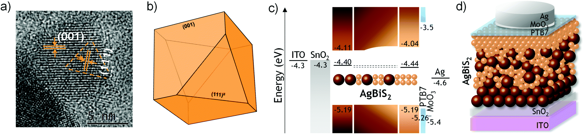 | ||
| Fig. 1 (a) HR-TEM image of a ∼10 nm AgBiS2 nanocrystal revealing the (001) and (111) lattice planes resembling the (b) optimal Wulff shape as predicted by Viñes et al.10 The matildite cubic structure features (001) facets, with only two cuts along the (111) direction. (c) Energy level diagram of the proposed device architecture. The light-absorbing layer is built in a gradient fashion, in which the first layer contains only large NCs, followed by 1 to n layers of mixed-size NCs and one last layer of only small NCs. (d) Schematic drawing of the cross-section of a photoactive device based on a mixture of small and large AgBiS2 nanocrystals. | ||
Besides the advantageous lower surface-to-volume ratio of the larger NCs, the other key difference between the two synthetic batches that motivated the present work is their moderate but appealing differences in the energy band alignment. Ultraviolet photoelectron spectroscopy (UPS) investigations concluded that the different sized NCs present a pinned valence band (−5.19 eV), and minor changes in the work function (Fig. S3†). On the contrary, the different energy bandgaps of the small (1.15 eV) and large (1.08 eV) NCs12 are responsible for the conduction band offset (Fig. 1c). We then recognized a parallelism with the work of Yang and co-workers, where the PbS quantum dot band alignment was intentionally shifted by mixing n- and p-type ligands. Therein, the promoted donor and acceptor domains favoured a more efficient interdot carrier transfer, thus resulting in a decreased recombination.16 In our work, the energy level engineering was done simply by using different sized AgBiS2 nanocrystals without modifying the iodide-based capping ligand. In particular, we took advantage from the layer-by-layer process to deposit photoactive layers with a gradient fashion in inverted architecture devices (Fig. 1d): a bottom layer of only large AgBiS2 NCs was coated on top of the electron transport layer (ETL) and followed by 1 to n layers of mixed-size NCs and an additional, top layer of only small NCs underneath the hole transport layer (HTL). In addition, such structures can provide a morphological benefit: the small NCs of the top layer fill the voids between the large NCs of the underneath mixed layers, which results in a smoother top layer topography and a potentially improved interface with the HTL. Such morphological improvement is visible in the nm scale (Fig. S4†); all the coated layers show a shiny aspect at a macroscopic scale. Overall, this architectural strategy has allowed us to build solar cells with a remarkable improvement in the power conversion efficiency as well as devices using thicker active layers that yielded promising photodetector performances.
Enhanced solar cell performance
In the past few years there has been a remarkable progress in the synthesis and application of colloidal AgBiS2 nanocrystals as the photoactive material in solar cell devices.7,11,12,17–23,24 The low carrier diffusion length and the non-negligible recombination pathways have been identified as the main limiting factors for photocurrent generation, especially when using thick active layers.7,12 Therefore, the record solar cell efficiencies reported so far typically limit the optimal AgBiS2 layer thickness at around 35 nm.Here, we started by fixing the same active layer thickness in mixed AgBiS2 solar cells as well as in the two control devices – employing only small and only large NCs (Fig. 2). In agreement with their dissimilar optical bandgaps, we observed a progressive drop in the VOC when changing the small NCs with mixed and large NCs (Table 1). In contrast, the average short-circuit current density (JSC) of the mixed NCs was as high as that obtained with the large NCs. The EQE spectra of the devices using mixed and only large NCs appeared to be almost identical, showing the expected red shift compared with the device using small NCs (Fig. 2c), as reported in our previous works.12 These data confirm that the JSC is strongly governed by the presence of the large NCs. Moreover, the use of mixed AgBiS2 NCs resulted in a ∼10% improvement in the fill factor (FF) with respect from the control devices, which is a signature of a more efficient charge transport. We ascribe this FF improvement primarily to the favourable cascade-type energy band structure25 of our proposed gradient fashion photoactive layer (Fig. 1c). Another set of control devices using the mixed NCs with the inverted gradient yielded statistically lower performances, especially due to lower fill factors (Fig. S5†). Additionally, the mixture of the small and large NCs helps to achieve a more balanced charge carrier mobility (Fig. S6†). These data further support the benefits of the proposed gradient. As a result, the PCE jumped from 6.5% and 6.3% for the control devices to a new record of 7.3% using mixed AgBiS2 nanocrystals, thus validating our strategy.
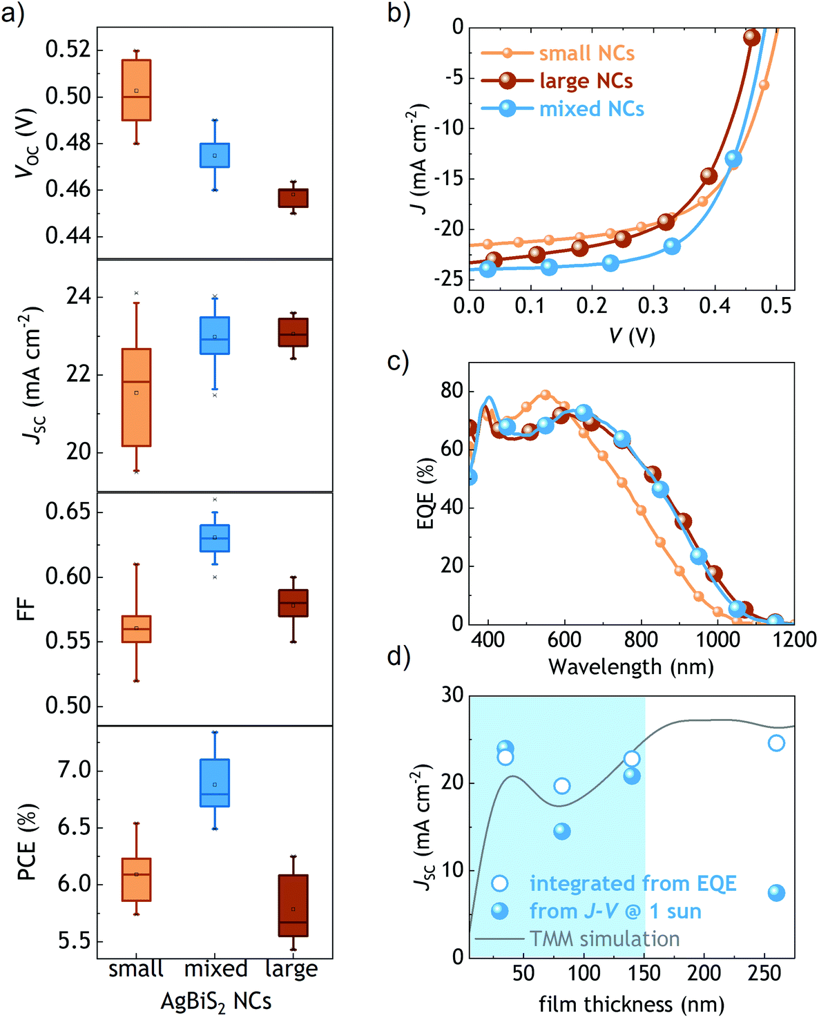 | ||
| Fig. 2 Photovoltaic performance of mixed AgBiS2 solar cells. (a) Statistical data of the open-circuit voltage (VOC), short-circuit current density (JSC), fill factor (FF) and power conversion efficiency (PCE) from devices based on small, large and mixed NCs. (b) JV characteristics of the best performing devices under 1 sun illumination conditions. (c) External quantum efficiency (EQE) spectrum of the best performing devices. (d) Influence of the photoactive layer thickness on the generated photocurrent. The shaded area defines the range of thicknesses where both the JSC under AM 1.5 G illumination (1 sun) and the JSC integrated from the external quantum efficiency spectra show a good match with the predicted values from the transfer-matrix model (solid line). Beyond that point, the recombination at high photon flux becomes stronger, and consequently the JSC at 1 sun deviates drastically from the predicted values. | ||
| AgBiS2 NCs | E g (eV) | V oc (V) | J sc (mA cm−2) | FF | PCE (%) |
|---|---|---|---|---|---|
| Small | 1.15 | 0.50 (0.50 ± 0.01) | 22.10 (21.54 ± 1.39) | 0.59 (0.56 ± 0.02) | 6.54 (6.09 ± 0.25) |
| Mixed | — | 0.48 (0.47 ± 0.01) | 23.97 (22.99 ± 0.66) | 0.64 (0.63 ± 0.01) | 7.33 (6.88 ± 0.25) |
| Large | 1.08 | 0.46 (0.46 ± 0.01) | 23.30 (23.06 ± 0.37) | 0.58 (0.58 ± 0.01) | 6.25 (5.78 ± 0.29) |
Then, we built thicker devices with the mixed NCs to evaluate the impact of the active layer thickness in photocurrent generation. Although the highest efficiency under 1 sun was still obtained with thin active layers (Fig. S7†), compared with our previous reports we did observe herein a significant improvement in the obtained photocurrent with thick active layers under low illumination conditions: for the first time, the JSC calculated from the integrated EQE spectra revealed a reasonably good match with our simulations made with a transfer-matrix model (Fig. 2d). The ∼260 nm thick device delivered an integrated JSC of 24.6 mA cm−2. These results motivated us to investigate the potential of mixed AgBiS2 nanocrystals in photodetector devices.
Thick AgBiS2 layers for photodetectors
In contrast to photovoltaics, the use of AgBiS2 nanocrystals in photodetector applications has been little studied.26,27 In this work, we fabricated devices with various absorbing layer thicknesses to explore the potential of this material as a broad bandwidth photodetector. We found that the record solar cell devices, based on a ∼35 nm thin active layer, delivered unsuitable, high dark currents. Upon increasing the thickness up to ∼260 nm, the dark current dropped between 2 and 3 orders of magnitude (Fig. 3). We ascribe this drop in the dark current to the prevention of shunt paths thanks to the layer thickness increase.28,29 Remarkably, the external quantum efficiency of that device remained above 60% within the 350–750 nm wavelength range and above 40% up to 1030 nm. The responsivity, which is proportional to the EQE at each wavelength,30 was found to peak at a wavelength of 1.01 μm with a value of 0.375 A W−1. In turn, the specific detectivity (D*, in cm Hz1/2 W−1 or Jones) was determined using eqn (1). | (1) |
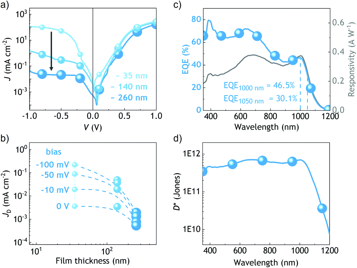 | ||
| Fig. 3 Photodetector performance of mixed AgBiS2 devices. (a) Dark JV characteristics of devices using different AgBiS2 layer thickness. (b) Dark current as a function of the photoactive layer thickness. The thickest device yielded the lowest dark current and best photodetector performance close to 0 V: (c) external quantum efficiency and responsivity spectra and (c) specific detectivity. | ||
Conclusions
We report herein an eco-friendly active ink based on mixed AgBiS2 colloidal nanocrystals that improves charge carrier extraction in photoactive layers. A tailored layer-by-layer process is implemented to build active layers with a gradient fashion, in which the mixture of small and large NCs intentionally facilitates the energy band alignment. Thanks to the enhanced charge transport, we construct solution-processed, thin film solar cells with higher fill factors and establish a new record power conversion efficiency of 7.3% for this semiconductor material. In addition, thicker devices that absorb more light demonstrate lower dark currents and specific detectivities above 3 × 10¹¹ Jones over the 350–1070 nm wavelength range, thus opening up new opportunities for AgBiS2 nanocrystals in the field of photodetectors.Author contributions
Conceptualisation, I. B.-C, G. K.; investigation, I. B.-C, Y. W; validation, Y. W; writing—original draft, I. B.-C; writing—review & editing, I. B.-C, G. K; supervision, G. K. The published version of the manuscript has been read and approved by all the authors.Lead contact
Further information and requests for resources and materials should be directed to and will be fulfilled by the lead contact, Gerasimos Konstantatos (gerasimos.konstantatos@icfo.eu).Data availability
The data that support this study are available from the lead contact upon reasonable request.Conflicts of interest
The authors declare no competing interests.Acknowledgements
G. K. acknowledges financial support from the European Research Council (ERC) under the European Union's Horizon 2020 research and innovation programme (grant agreement no. 725165) and the Fundació Joan Ribas Araquistain (FJRA). This project was supported also by Fundació Privada Cellex, the program CERCA, EQC2019-005797-P (AEI/FEDER UE), 2017SGR1373 and “Severo ochoa” Center of Excellence CEX2019-000910-S – Funded by the Spanish State Research Agency. Y. W. acknowledges the support from the European Union's Horizon 2020 research and innovation programme under the Marie Skłodowska-Curie grant agreement No. 754558. I. Burgués-Ceballos acknowledges support from the Government of Catalonia's Beatriu de Pinós postdoctoral programme (grant number 2017BP00241).Notes and references
- C. R. Kagan, E. Lifshitz, E. H. Sargent and D. V. Talapin, Building Devices from Colloidal Quantum Dots, Science, 2016, 353, aac5523, DOI:10.1126/science.aac5523
.
- M. J. Choi, F. P. García de Arquer, A. H. Proppe, A. Seifitokaldani, J. Choi, J. Kim, S. W. Baek, M. Liu, B. Sun, M. Biondi, B. Scheffel, G. Walters, D. H. Nam, J. W. Jo, O. Ouellette, O. Voznyy, S. Hoogland, S. O. Kelley, Y. S. Jung and E. H. Sargent, Cascade Surface Modification of Colloidal Quantum Dot Inks Enables Efficient Bulk Homojunction Photovoltaics, Nat. Commun., 2020, 11(1), 1–9, DOI:10.1038/s41467-019-13437-2
- M. G. Panthani, J. M. Kurley, R. W. Crisp, T. C. Dietz, T. Ezzyat, J. M. Luther and D. V. Talapin, High Efficiency Solution Processed Sintered CdTe Nanocrystal Solar Cells: The Role of Interfaces, Nano Lett., 2014, 14(2), 670–675, DOI:10.1021/nl403912w
- M. Hao, Y. Bai, S. Zeiske, L. Ren, J. Liu, Y. Yuan, N. Zarrabi, N. Cheng, M. Ghasemi, P. Chen, M. Lyu, D. He, J. H. Yun, Y. Du, Y. Wang, S. Ding, A. Armin, P. Meredith, G. Liu, H. M. Cheng and L. Wang, Ligand-Assisted Cation-Exchange Engineering for High-Efficiency Colloidal Cs1−xFAxPbI3 Quantum Dot Solar Cells with Reduced Phase Segregation, Nat. Energy, 2020, 5(1), 79–88, DOI:10.1038/s41560-019-0535-7
- Y. E. Romanyuk, H. Hagendorfer, P. Stücheli, P. Fuchs, A. R. Uhl, C. M. Sutter-Fella, M. Werner, S. Haass, J. Stückelberger, C. Broussillou, P. P. Grand, V. Bermudez and A. N. Tiwari, All Solution-Processed Chalcogenide Solar Cells - From Single Functional Layers Towards a 13.8% Efficient CIGS Device, Adv. Funct. Mater., 2015, 25(1), 12–27, DOI:10.1002/adfm.201402288
- J. Kim, H. Hiroi, T. K. Todorov, O. Gunawan, M. Kuwahara, T. Gokmen, D. Nair, M. Hopstaken, B. Shin, Y. S. Lee, W. Wang, H. Sugimoto and D. B. Mitzi, High Efficiency Cu2ZnSn(S,Se)4 Solar Cells by Applying a Double In2S3/CdS Emitter, Adv. Mater., 2014, 26(44), 7427–7431, DOI:10.1002/adma.201402373
- M. Bernechea, N. C. Miller, G. Xercavins, D. So, A. Stavrinadis and G. Konstantatos, Solution-Processed Solar Cells Based on Environmentally Friendly AgBiS2 Nanocrystals, Nat. Photonics, 2016, 10(8), 521–525, DOI:10.1038/nphoton.2016.108
- F. Viñes, G. Konstantatos and F. Illas, Bandgap Engineering by Cationic Disorder: Case Study on AgBiS2, Phys. Chem. Chem. Phys., 2017, 19, 27940–27944, 10.1039/C7CP05118B
- F. Viñes, M. Bernechea, G. Konstantatos and F. Illas, Matildite versus Schapbachite: First-Principles Investigation of the Origin of Photoactivity in AgBiS2, Phys. Rev. B, 2016, 94, 235203, DOI:10.1103/PhysRevB.94.235203
- F. Viñes, G. Konstantatos and F. Illas, Matildite Contact with Media: First-Principles Study of AgBiS2Surfaces and Nanoparticle Morphology, J. Phys. Chem. B, 2018, 122(2), 521–526, DOI:10.1021/acs.jpcb.7b03967
- M. Z. Akgul, A. Figueroba, S. Pradhan, Y. Bi and G. Konstantatos, Low-Cost RoHS Compliant Solution Processed Photovoltaics Enabled by Ambient Condition Synthesis of AgBiS2 Nanocrystals, ACS Photonics, 2020, 7(3), 588–595, DOI:10.1021/acsphotonics.9b01757
- I. Burgués-Ceballos, Y. Wang, M. Z. Akgul and G. Konstantatos, Colloidal AgBiS2 Nanocrystals with Reduced Recombination Yield 6.4% Power Conversion Efficiency in Solution-Processed Solar Cells, Nano Energy, 2020, 75, 104961, DOI:10.1016/j.nanoen.2020.104961
- T. Kirchartz, F. Deledalle, P. S. Tuladhar, J. R. Durrant and J. Nelson, On the Differences between Dark and Light Ideality Factor in Polymer:Fullerene Solar Cells, J. Phys. Chem. Lett., 2013, 4(14), 2371–2376, DOI:10.1021/jz4012146
- S. R. Cowan, A. Roy and A. J. Heeger, Recombination in Polymer-Fullerene Bulk Heterojunction Solar Cells, Phys. Rev. B: Condens. Matter Mater. Phys., 2010, 82(24), 1–10, DOI:10.1103/PhysRevB.82.245207
- Y. Cao, A. Stavrinadis, T. Lasanta, D. So and G. Konstantatos, The Role of Surface Passivation for E_cient and Photostable PbS Quantum Dot Solar Cells, Nat. Energy, 2016, 1, 16035, DOI:10.1038/NENERGY.2016.35
- Z. Yang, J. Z. Fan, A. H. Proppe, F. P. García de Arquer, D. Rossouw, O. Voznyy, X. Lan, M. Liu, G. Walters, R. Quintero-bermudez, B. Sun, S. Hoogland, G. A. Botton, S. O. Kelley and E. H. Sargent, Mixed-Quantum-Dot Solar Cells, Nat. Commun., 2017, 8, 1325, DOI:10.1038/s41467-017-01362-1
- P. Huang, W. Yang and M. Lee, AgBiS2 Semiconductor-Sensitized Solar Cells, J. Phys. Chem. C, 2013, 117, 18308–18314 CrossRef CAS
- N. Pai, J. Lu, D. C. Senevirathna, A. S. R. Chesman, T. Gengenbach, M. Chatti, U. Bach, P. C. Andrews, L. Spiccia, Y. Cheng and A. N. Simonov, Spray Deposition of AgBiS2 and Cu3BiS3 Thin Films for Photovoltaic Applications, J. Mater. Chem. C, 2018, 6, 2483–2494, 10.1039/C7TC05711C
- J. T. Oh, S. Y. Bae, S. R. Ha, H. Cho, S. J. Lim, D. W. Boukhvalov, Y. Kim and H. Choi, Water-Resistant AgBiS2 Colloidal Nanocrystal Solids for Eco-Friendly Thin Film Photovoltaics, Nanoscale, 2019, 11, 9633–9640, 10.1039/c9nr01192g
- S. Y. Bae, J. T. Oh, J. Y. Park, S. R. Ha, J. Choi, H. Choi and Y. Kim, Improved Eco-Friendly Photovoltaics Based on Stabilized AgBiS2 Nanocrystal Inks, Chem. Mater., 2020, 32(23), 10007–10014, DOI:10.1021/acs.chemmater.0c03126
- J. T. Oh, H. Cho, S. Y. Bae, S. J. Lim, J. Kang, I. H. Jung, H. Choi and Y. Kim, Improved Size Distribution of AgBiS2 Colloidal Nanocrystals by Optimized Synthetic Route Enhances Photovoltaic Performance, Int. J. Energy Res., 2020, 44, 11006–11014, DOI:10.1002/er.5695
- V. A. Öberg, M. B. Johansson, X. Zhang and E. M. J. Johansson, Cubic AgBiS2Colloidal Nanocrystals for Solar Cells, ACS Appl. Nano Mater., 2020, 3, 4014–4024, DOI:10.1021/acsanm.9b02443
- Y. Xiao, H. Wang, F. Awai, N. Shibayama, T. Kubo and H. Segawa, Eco-Friendly AgBiS2 Nanocrystal/ZnO Nanowire Heterojunction Solar Cells with Enhanced Carrier Collection Efficiency, ACS Appl. Mater. Interfaces, 2021, 13, 3969–3978, DOI:10.1021/acsami.0c19435
- S. Zhou, J. Yang, W. Li, Q. Jiang, Y. Luo, D. Zhang, Z. Zhou and X. Li, Preparation and Photovoltaic Properties of Ternary AgBiS2 Quantum Dots Sensitized TiO2 Nanorods Photoanodes by Electrochemical Atomic Layer Deposition, J. Electrochem. Soc., 2016, 163(3), 63–67, DOI:10.1149/2.0161603jes
- C. You, G. Zhang, W. Deng, C. Zhao, B. An, B. Liu, B. Wang, H. Yan, D. Liu and Y. Zhang, Cascade-Type Energy Band Design of a Black Phosphorus Photodetector with High Performance, J. Mater. Chem. C, 2019, 7, 2232, 10.1039/c8tc05735d
- C. H. Mak, J. Qian, L. Rogée, W. K. Lai and S. P. Lau, Facile Synthesis of AgBiS2 Nanocrystals for High Responsivity Infrared Detectors, RSC Adv., 2018, 8, 39203, 10.1039/c8ra08509a
- L. Jiang, Y. Li, J. Peng, L. Cui, R. Li, Y. Xu, W. Li, Y. Li, X. Tian and Q. Lin, Solution-Processed AgBiS2 Photodetectors from Molecular Precursors, J. Mater. Chem. C, 2020, 8, 2436, 10.1039/c9tc06499k
- P. E. Keivanidis, P. K. H. Ho, R. H. Friend and N. C. Greenham, The Dependence of Device Dark Current on the Active Layer Morphology of Solution-Processed Organic Photodetectors, Adv. Funct. Mater., 2010, 20, 3895–3903, DOI:10.1002/adfm.201000967
- Z. Tang, Z. Ma, A. Sánchez-Díaz, S. Ullbrich, Y. Liu, B. Siegmund, A. Mischok, K. Leo, M. Campoy-Quiles, W. Li and K. Vandewal, Polymer:Fullerene Bimolecular Crystals for Near–Infrared Spectroscopic Photodetectors, Adv. Mater., 2017, 29, 1702184 CrossRef PubMed
- Y. Fang, A. Armin, P. Meredith and J. Huang, Accurate Characterization of Next-Generation Thin-Film Photodetectors, Nat. Photonics, 2019, 13, 1–4, DOI:10.1038/s41566-018-0288-z
- Z. Wu, Y. Zhai, H. Kim, J. D. Azoulay and T. N. Ng, Emerging Design and Characterization Guidelines for Polymer- Based Infrared Photodetectors, Acc. Chem. Res., 2018, 51, 3144–3153, DOI:10.1021/acs.accounts.8b00446
- G. Konstantatos, Current Status and Technological Prospect of Photodetectors Based on Two-Dimensional Materials, Nat. Commun., 2018, 9, 5266, DOI:10.1038/s41467-018-07643-7
Footnote |
| † Electronic supplementary information (ESI) available: Details of the materials, syntheses, and device preparation and characterisation methods. See DOI: 10.1039/d2nr00589a |
| This journal is © The Royal Society of Chemistry 2022 |