
 Open Access Article
 This Open Access Article is licensed under a Creative Commons Attribution-Non Commercial 3.0 Unported Licence
Electromechanical conversion efficiency of GaN NWs: critical influence of the NW stiffness, the Schottky nano-contact and the surface charge effects†
Noelle
Gogneau
 *a,
Pascal
Chrétien
b,
Tanbir
Sodhi
ab,
Laurent
Couraud
a,
Laetitia
Leroy
a,
Laurent
Travers
a,
Jean-Chistophe
Harmand
a,
François H.
Julien
a,
Maria
Tchernycheva
a and
Frédéric
Houzé
b
*a,
Pascal
Chrétien
b,
Tanbir
Sodhi
ab,
Laurent
Couraud
a,
Laetitia
Leroy
a,
Laurent
Travers
a,
Jean-Chistophe
Harmand
a,
François H.
Julien
a,
Maria
Tchernycheva
a and
Frédéric
Houzé
b
aCentre de Nanosciences et Nanotechnologies, Université Paris-Saclay, CNRS, UMR9001, Boulevard Thomas Gobert, 91120 Palaiseau, France. E-mail: noelle.gogneau@c2n.upsaclay.fr
bUniversité Paris-Saclay, CentraleSupélec, Sorbonne Université, CNRS, Laboratoire de Génie électrique et électronique de Paris, 11 rue Joliot-Curie, 91190 Gif sur Yvette, France
First published on 17th March 2022
Abstract
The piezoelectric nanowires (NWs) are considered as promising nanomaterials to develop high-efficient piezoelectric generators. Establishing the relationship between their characteristics and their piezoelectric conversion properties is now essential to further improve the devices. However, due to their nanoscale dimensions, the NWs are characterized by new properties that are challenging to investigate. Here, we use an advanced nano-characterization tool derived from AFM to quantify the piezo-conversion properties of NWs axially compressed with a well-controlled applied force. This unique technique allows to establish the direct relation between the output signal generation and the NW stiffness and to quantify the electromechanical coupling coefficient of GaN NWs, which can reach up to 43.4%. We highlight that this coefficient is affected by the formation of the Schottky nano-contact harvesting the piezo-generated energy, and is extremely sensitive to the surface charge effects, strongly pronounced in sub-100 nm wide GaN NWs. These results constitute a new building block in the improvement of NW-based nanogenerator devices.
Introduction
Thanks to their large surface-to-volume ratio, high crystalline quality and nanometer scale dimensions, semiconductor nanowires (NWs) offer unique advantages for a wide range of applications.1–5 In particular, NWs presenting piezoelectric properties appear as promising active nanostructures for a new generation of piezoelectric sensors6–10 and harvesters.11–15 Especially, the sub-100 nm-wide NWs present the particularity to exhibit novel properties, non-existing or non-significant at micrometric scales that can lead to a strong modulation/modification of their characteristics. The exaltation of the piezoelectric coefficients,16–18 the modulation of the free carrier concentration19,20 or the formation of nano-contact at the NW/electrode interface21 are examples of these nanoscale phenomena. In-depth understanding of these new properties is crucial to take full advantage of the 1D-nanostructures and thus develop high-efficiency NW-based devices.However, characterization at the nanoscale is challenging, especially when dealing with the electrical properties. Indeed, the usual methods are often unsuitable for NWs. The development of new nano-characterization techniques is required.
For piezoelectric properties, the atomic force microscope (AFM) equipped with the piezo-response scanning mode (reverse piezoelectric effect) allows to quantify the piezoelectric coefficients of single connected 1D-nanostructures, such as NWs16 or nanofibers.22 By contrast, the characterization of piezoelectric conversion properties of NWs (direct piezoelectric effect) is challenging since no commercial system is available. In recent years, the piezoelectrical generation from various single 1D-nanostructures has been demonstrated by laterally bending them using in-house-AFM systems.23–27 Although this experimental approach allows quantifying the output voltage (OV) generation capacity, it does not give access to the mechanical behavior of the nanostructures. In addition, the induced lateral bending does not reflect the main deformation undergone by the 1D-nanostructures integrated into the devices, which are mainly deformed axially.
In situ SEM and TEM techniques have also been recently used to study the electromechanical properties of InAs,28,29 ZnO30 or BaTiO331 NWs. The main advantage of these techniques relies in the possible correlation of the piezoelectric properties of the investigated nanostructures, with their mechanical deformation, as well as their crystal structure, size or defects. However, following this characterization methodology, the nanostructures are transferred from their growth substrate and individually connected. It is thus difficult to establish an electromechanical behavior in a statistic way. Moreover, the experiments are performed under vacuum, which modulates the concentration of surface charges, known to affect the free carrier concentration within the materials and thus the screening of the piezo-charges.20,32 The conditions are, in these specific situations, non-representative of the ones met in the devices.
Today, establishing a direct correlation between the mechanical and piezoelectrical properties, in a configuration compatible with the device one, is of crucial importance to further improve NW-based device architectures and performances. To quantify direct piezoelectric measurement in device compatible conditions, we use a unique advanced nano-characterization tool based on AFM probing the piezo-conversion properties of GaN NWs axially compressed with a well-controlled applied force. The choice of the III-Nitride materials and more specifically of the GaN NWs is motivated by their high-piezoelectric conversion capacities. In fact, the output signals generated by III-N NWs in response to an external mechanical input exceed the ones obtained with other piezoelectric 1D-nanostructures, such as CdS,24 CdSe,25 PZT,26 BaTiO3,31 KNBO3,33 GaAs34 and even ZnO35,36 which is today the most widely used semiconductor in the NW-based piezo-generators. Hence, for a single nanowire, outputs ranging from several tens of millivolts (mV) to several hundreds of mV (up to 550 mV) for GaN27,37 have been measured, while output voltages for ZnO NWs does not exceed 90 mV per NW.36 With our unique instrument, we can measure simultaneously and thus correlate the OV generated by each NW of the array and its NW deformation rate. In other words, we can access the piezo-conversion of a large number of individual NWs and establish a general behavior on a statistically representative ensemble of nanostructures. Thus, for the first time, we are able to establish experimentally the relation between the OV generation and the NW stiffness, and we can quantify the electromechanical coupling coefficient of GaN NWs. We demonstrate that this coefficient reaches up to 43.4% and is extremely sensitive to nanometer scale phenomena. Especially, we show that this coefficient is affected by the formation of the Schottky nano-contact21 through which the piezo-generated energy is harvested; and by the expression of the surface charge effects, which are known to have an important impact for sub-100 nm wide GaN NWs.38
Methodology
Today, the most common method to measure direct piezoelectric response of vertically oriented 1D-nanostructures uses in-house-AFM equipped with an electrical module. The conductive AFM tip, operating in the usual contact mode, induces a local deformation of the nanostructure, while simultaneously measuring the generated electric potential resulting from its deformation. To ensure the piezoelectric charge collection, this technique is based on the combination of an Ohmic and a Schottky contact formed respectively at the substrate/nanostructure and nanostructure/conductive AFM tip (electrode) interfaces39,40 (ESI S1†). These measurements are performed without any external polarization.23,27In all reported measurements, the AFM tip always induces a lateral bending of the NW. This local deformation produces an internal piezoelectric field within the NW, which generates an output electrical signal (ESI S2†).23,27,41,42 However, the bending, which increases with the applied force is high, is extremely difficult to quantify from a mechanical point of view: the effective local force consists of two mixed components (normal and lateral), which are difficult to quantify in scanning mode. This results in even more complex mechanical response combining compression and bending. In these conditions, it is not straightforward to establish a correlation between the electrical and mechanical properties of the NWs and thus improve their electromechanical coupling, therefore the piezo-generator device efficiency. Furthermore, due to the NW-based device architecture and the type of applied deformation, the nanostructures are mainly deformed axially, so studies under bending are irrelevant for practical applications. The usual AFM technique is thus not well suited for correlating the properties of single NWs with the NW-based device performances.
To simultaneously characterize the piezoelectric and mechanical properties of 1D-nanostructures under conditions reflecting their deformations experienced in real devices, we use an unique AFM module based on a conducting probe AFM system working in an intermittent contact mode (Fig. 1a) inspired by the so-called ‘pulsed force mode’ (PFM), a low frequency non-resonant mode originally developed for local mechanical measurements.43 On this method, some modifications have been performed in order to allows us quantifying the piezoelectric response of individual NWs under a well-controlled and purely axial force. Where the z-piezo supports the NW sample, the technique consists in introducing a sinusoidal modulation on the AFM z-piezo at a frequency between 100 Hz and 2 kHz (i.e. far below the cantilever fundamental resonance), in order to oscillate in close proximity to the probe so that the tip furtively hits the sample surface at each period. The oscillation amplitude is adjusted so that the tip alternates contact and non-contact every cycle. The maximum repulsive force is measured from the deflection signal and is used as a feedback parameter, ensuring well-controlled scan conditions. The main advantages of this approach are: (i) the friction is considerably reduced compared with the classical permanent contact mode; and (ii) the low operating frequency leaves enough time to properly measure physical parameters simultaneously such as the generated OV and the topography during each cycle. Thus, AFM characterization of soft samples becomes possible and it is therefore applicable to sub-100 nm wide NWs.
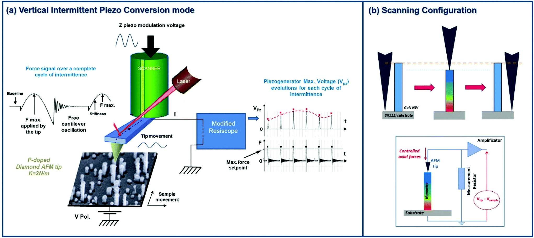 | ||
| Fig. 1 (a) Schematic view of the new conducting AFM technique working in intermittent-contact piezoelectric mode, inspired by the so-called ‘pulsed force mode’ (PFM). Combined with a specifically adapted Resiscope module, the AFM system allows quantifying the piezoelectric response of individual GaN NWs resulting from their deformation under a well-controlled axial normal force; (b) schematic views of the measurement principle and of the equivalent electrical circuit of the AFM system. | ||
To perform electrical measurements in such intermittent mode, we associated the PFM-type actuation with a specifically adapted version of our conversion and amplification Resiscope44 module (allowing dynamic resistance measurements over a very wide range (102–1012 Ω)) previously used in standard contact mode.27 In particular, we brought the possibility to precisely define, for each intermittency cycle, the moment at which the electrical information is collected during the brief contact duration when the tip applies a controlled normal force on the NW. As a result, due to the near absence of friction, we can image only the voltage generated by the pure axial force exerted by the tip on each NW (Fig. 1b). As for the classical AFM contact mode, the charge collection is ensured with ohmic/Schottky base/top contacts and without any external polarization of the nanostructures. However, in this experimental configuration, the piezo-generated energy is harvested through an intermittent and fast electric contact. To ensure reliable electrical measurements,21 the investigated samples have been technologically prepared.
Firstly, the NWs have been mechanically consolidated. In fact, the investigated p-doped GaN NWs, grown by plasma assisted molecular beam epitaxy are characterized by sub-100 nm wide diameters (Fig. 2a) and by a strong flexibility.27 In consequence, a small constant normal force of few nN is sufficient for folding up the NWs towards the substrate surface or the neighbouring NWs, and inducing a leakage of the piezoelectric charges created inside the NWs in response to its deformation. In addition, these extreme deformations of the NWs do not allow the establishment of a stable AFM tip/NW contact required for performing reliable electrical measurements. To circumvent these problems, the mechanical resistance of the NWs was increased by partially embedding their base into a polymethyl methacrylate (PMMA) resist layer as schematized in Fig. 2b and c.
 | ||
| Fig. 2 (a) GaN NWs grown by plasma-assisted molecular beam epitaxy; (b–d) schematic representation of the preparation for the GaN NW sample for AFM measurements. HNW-init, HEmbed.-NW and Hresist define respectively the initial NW height, the protruding NW height after consolidation and the resist height; (e) SEM images of tilted top view and cross-section view of the electrically connected NWs with a thin 5 nm-Cr/20 nm-Pt Schottky electrode directly deposited on the top of each NW forming the array. | ||
Secondly, the quality and stability of the electrical contact are crucial.21,45 Because the contact with the NW top is established under fast conditions, potential instability of the contact can affect the measurement.45 To circumvent this problem, instead of using the NW/tip interface as in the conventional AFM approach,23,27 the Schottky contact is delocalized by depositing directly on the NW top a thin 5 nm-Cr/20 nm-Pt top electrode (Fig. 2d). As we can see on Fig. 2e, the top electrode is localized on the NW tips without forming a continuous layer on their edges. Only isolated particles of metal are visible on their edges. This configuration thus avoids connecting the residual metallic film deposited on the PMMA top, and allows to ensure to the top deposition the role of electrode to harvest the piezo-generated output signal. The cross-section view shows well how the bottom of the NWs are embedded into the PMMA matrix, while their emerging part is characterized by the Schottky electrode localized on their top. Thus, thanks to the presence of this specific top electrode, a metal/metal contact is thus formed between the conductive p-type doped diamond AFM tip and the NW, leading to a more stable contact and thus a more efficient energy harvesting under fast AFM scanning conditions.
Following our unique experimental configuration, the GaN NWs are axially deformed. Under this vertical compression input, a positive piezo-potential in created in the top portion of the NW41 (ESI S3†), where the deformation is the strongest. The investigated GaN nanostructures being slightly p-doped (cf. Methods), the Schottky diode is positively biased and thus allows collecting the positive output signal.41,46 In addition, because the topographic and electrical signals are simultaneously recorded under a well-controlled axial deformation, it is thus possible to directly correlate the mechanical properties of the NWs and their piezo-conversion properties.
Results and discussion
Piezo-conversion measurements
The electromechanical coupling properties of GaN NWs are investigated under a well-controlled axial compressive force (defined as the constant normal force, CNF) evolving between 40 and 220 nN (Fig. 3). The 2D mappings of output voltage (OV) peaks generated by each NW of the array (Fig. 3b) experimentally demonstrate, for the first time, the piezoelectric response of individual NWs under axial mechanical input. Equivalent to NWs investigated by AFM under bending,27,42 and in agreement with the theoretical predictions,47 the direct piezoelectric effect is demonstrated: the OV generation increases with the axial applied force. The statistical analysis of the electrical mappings (Fig. 3c), approximated by Gaussian functions (Fig. 3d), details the variation of the average and maximum OV as a function of the CNF (table of values is presented in ESI Table S1†). Especially, it evidences a bimodal distribution of the average OV values. | ||
| Fig. 3 (a) (10 μm × 5 μm) topographic AFM image recorded for an applied force, so-called Constant Normal Force (CNF), of 180 nN. The colour dispersion illustrates the distribution in height resulting from the self-assembled growth mode used to synthesize the GaN NWs; (b) (10 μm × 5 μm) 2D mappings of OV generated by GaN NWs in response to an axial compression induced by the AFM tip with a CNF of 60, 100, 140 and 180 nN; (c) statistical analysis of 2D electrical mappings for an applied force evolving in the 40–220 nN range. A bimodal distribution of the averaged OV is evidenced as it is clearly visible in (d), showing examples of the OV distribution for three CNFs, approximated with Gaussian functions. | ||
The piezo-response of NWs is directly related to their degree of deformation, which itself strongly depends on their dimensions. In the present study, NWs are synthesized following the self-assembled growth mode. The nanostructures are thus characterized by a small dispersion in terms of height and diameter, which results in a dispersion of flexibility/stiffness. This dispersion allows spanning a significant range of stiffness values within one sample. Thereby, we could establish experimentally the intrinsic relation between the piezo-generated OV and the NW stiffness (Fig. 4) for three CNFs (80, 120 and 160 nN).
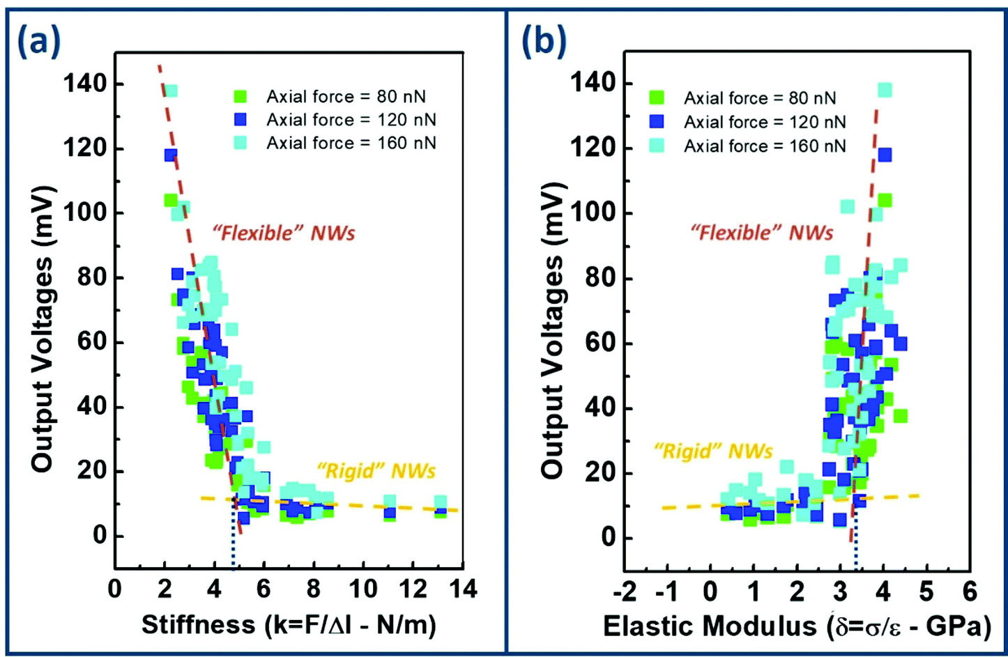 | ||
| Fig. 4 Variation of the OV piezo-generated by the GaN NWs as a function of their stiffness for three applied axial forces. The stiffness has been quantified following the Hooke's Law (a) and the elasticity modulus definition (b). Whatever the used quantification method, for a given force, two different regimes are distinguished: “rigid” NWs, defined by a stiffness higher than ∼5 N m−1 (δ lower than ∼3.5 GPa), and “flexible” NWs, defined by a stiffness lower than ∼5 N m−1 (δ higher than ∼3.5 GPa). | ||
The stiffness has been quantified by using the experimental NW height variation (Δl) in response to the action of the CNF (F). The F = f(Δl) plot (ESI S4†) shows a linear dependence for low to moderate CNFs (≤200 nN). The y-axis intercept of the linear part corresponds to the initial NW height and its slope represents the NW stiffness (k, in the unit of Nm−1) which indeed follows the Hooke's law, F = k·Δl. At higher F and for the NWs of lower stiffness, the data deviate from the ideal Hooke's law, Δl being larger than expected. This indicates that these NWs start to bend under the action of the CNF (ESI S4†). The stiffness can also be considered through the elastic modulus quantity, defined as the ratio between stress and strain: δ (Pa) = σ/ε (ESI S4†). Quantified with this method, the stiffness presents equivalent dependence with the CNFs.
Both experimental OV-k (Fig. 4a) and OV-δ (Fig. 4b) relations evidence the direct piezoelectric effect: the more important is the NW deformation (directly linked to its stiffness), the higher is the OV generation. Nevertheless, two regimes can be distinguished. For high-k (low-δ) NWs, called “rigid” NWs (k ≳ 5 Nm−1 or δ ≲ 3.5 GPa), the OV only weakly varies with stiffness. The NWs are characterized by a high rigidity, which limits their degree of compression under a given CNF and thus prevents the creation of a strong piezoelectric field. By contrast, for low-k (high-δ) NWs, called “flexible” NWs (k ≲ 5 Nm−1 or δ ≳ 3.5 GPa), the OV steeply increases by more than one decade. The NWs being more flexible, it is easier, under an equivalent CNF, to create a higher piezoelectric field and thus generate a stronger OV. These two distinct regimes correspond to the OV bimodal distribution observed on Fig. 3c: the first (second) distribution is related to the “rigid” (“flexible”) NWs.
The piezoelectric mechanism is conceptually illustrated in Fig. 5. Therefore, the difference in the OV variation slope between the two regimes probably refers to a different mode of deformation. While for “rigid” NWs, we can assume a purely axial deformation (Fig. 5a), for “flexible” NWs, a deformation combining axial compression and a slight buckling of the NW body is more likely. Thus, for an equivalent CNF, the resulting strain field within the “flexible” NWs is more complex than in “rigid” NWs, and their deformation is more important. In this case, the proportion of buckling, which depends on the NW aspect ratio48,49 plays a critical role in the NW piezo-response. For k in the [3–5 Nm−1] range (or δ in the [3.5–4 GPa] range), we assume that a soft buckling occurs via twinning/twisting along the NW body, as observed and simulated in 1D-nanostructues.49–51 This deformation mechanism tends to add compression in the NW,49,52 leading to an enhanced positive piezo-potential and thus to a higher piezo-generation (Fig. 5b). Due to the high flexibility of GaN NWs,27 and because the applied deformation does not exceed few percents, the buckling deformation is assumed to be reversible.50,53 This reversibility is supported by the integrity of NW piezo-response, non drastically decreased or disappeared with the successive measurements (Fig. 3). By contrast, for NW stiffness lower than 3 Nm−1 (elastic modulus higher than 4 GPa) and for a strong CNF, we assume a stronger buckling with a portion of the NW being laterally bended (Fig. 5c). In this case, the NW presents a complex distribution of the strain field with tensile and compression regions54 (ESI S2†). In consequence, the internal piezoelectric field is not characterized only by a positive value (case when the wire is fully compressed) which will increase with the degree of compression. It is characterized by the sum of a positive field created within the compressive portion of the NW and a negative field created within the tensile portion of the NW. The total piezo-potential is then lowered and thus leads to a reduced output signal. The onset of this regime is experimentally confirmed by the piezo-response plotted in Fig. 3c. While the average OV of the first NW population (the “rigid” NWs) increases continuously with the CNF, the average OV of the second population (the “flexible” NWs) and the maximum OV generation increase before decreasing for CNF higher than 200 nN.
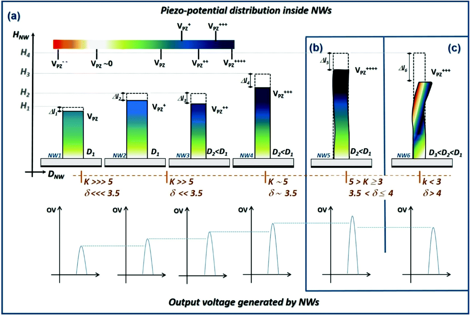 | ||
| Fig. 5 Schematic representation of the piezoelectric field distribution within the GaN NWs and the corresponding output signal generated in response to an equivalent axial mechanical input as a function of the nanostructure stiffness/elastic modulus (linked to the NW diameter D and height H). k and δ are respectively expressed in Nm−1 and in GPa. Δl illustrates the NW height variation in response to its deformation. (a) For NW stiffness higher than ∼5 Nm−1 (elastic modulus lower than 3.5 GPa), the deformation is purely compressive. The degree of compression, and thus the resulting piezoelectric field created within the nanostructure, increases with the NW stiffness decrease; (b) for stiffness in the [3–5 Nm−1] range (elastic modulus in the [3.5–4 GPa] range), a soft reversible buckling occurs via twinning/twisting along the NW body which tends to add compression in the NW and thus leads to an enhanced piezoelectric generation. (c) For NW stiffness lower than 3 Nm−1 (elastic modulus higher than 4 GPa) and for a strong CNF, a stronger buckling occurs with a portion of the NW being laterally bent. This results in a reduced strain state, leading to a lowered piezo-potential and thus a reduced output signal. | ||
Results displayed in Fig. 3 and 4 thus experimentally establish that the double OV distribution of our NWs is linked to their stiffness and their deformation modes.
In the specific case of high flexible NWs, our estimation of their stiffness is most certainly underestimated. In order to avoid any ambiguity, only the NWs with a stiffness ≥5 Nm−1 (elastic modulus lower than 3.5 GPa), thus being purely axially compressed, will be considered in the following of the manuscript.
Figure of merit: Eelectromechanical coupling coefficient
Currently, in the literature, the value of OV is considered to quantify the piezo-conversion capacity of NWs, which is not entirely rigorous. For the sake of comparison, we provide the OV values measured in this study under a purely axial compression. The values, reported in Table 1 for CNFs of 100 and 200 nN, equalize, or even exceed, those generated by various unique 1D-nanostructures, such as ZnS,55 CdS,56 CdSe,57 CdTe58 and ZnO nanowires,34,35 while they are tested under AFM according to the “classic” mode leading to a stronger deformation for an equivalent applied CNF (ESI S1†).| CNF | 100 nN | 200 nN | ||
|---|---|---|---|---|
| Rigid NWs (1st distribution) | Flexible NWs (2nd distribution) | Rigid NWs (1st distribution) | Flexible NWs (2nd distribution) | |
| Average OV (mV) | 16 | 54 | 29 | 88 |
| Maximum OV (mV) | 111 | 159 | ||
| Average output power density (mW cm−2) | 0.20 | 2.33 | 0.67 | 6.20 |
| Maximum output power density (mW cm−2) | 9.86 | 20.22 | ||
To illustrate the powering capacity of the NWs axially compressed (deformation compatible with device conditions), the following equation is used: 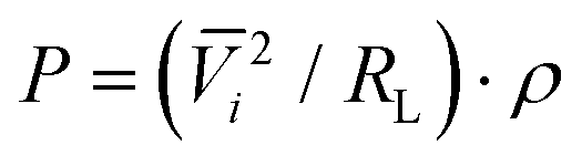 , where Vi is the output voltage generated by the i-th NW, RL is the resistance across which the measurement is performed (RL = 1 GΩ) and ρ is the surface density of NWs (8 × 10⁸ NW cm−2 in the present study). The results, also reported in the Table 1, give an idea of the potential of GaN NW as building blocks of high-efficient nano-piezo-generators.
However, the OV cannot be a universal criterion since its values are sensitive to the deformation mode, the applied force, the load resistance and the electronic measurement system. It is thus extremely difficult to compare different systems and misleading to discuss the piezo-conversion capacity by considering only this parameter.
The best evaluation of the real potential of NWs consists in quantifying the electromechanical coupling coefficient defined by:
 | (1) |
The output electric energy generated by an individual NW in one piezoelectric discharge is given by (ESI S5†):
 | (2) |
The input mechanical energy, corresponding to the elastic deformation energy for axially compressing/releasing the NW is given by (ESI S5†):
| ΔWElast. = FΔl | (3) |
The electromechanical coupling has been estimated for several individual NWs (k ≥ 5 Nm−1) deformed under a pure axial compression (Table 2). This estimation has been performed for a NW deformation of 1%.
| NW stiffness (N m−1) | Output voltage (mV) | Electo-mechanical coupling coefficient (%) | NW stiffness (N m−1) | Output voltage (mV) | Electo-mechanical coupling coefficient (%) | NW stiffness (N m−1) | Output voltage (mV) | Electo-mechanical coupling coefficient (%) |
|---|---|---|---|---|---|---|---|---|
| 4.9 | 13.1 | 31 | 5.6 | 7.9 | 9.9 | 7.8 | 6.8 | 7.8 |
| 4.9 | 11.6 | 29.1 | 5.9 | 6.9 | 20.4 | 8.1 | 7.5 | 9.4 |
| 4.9 | 15.2 | 43.4 | 5.9 | 8.6 | 15.5 | 8.6 | 5.8 | 5.9 |
| 5.0 | 14.2 | 35.5 | 6.0 | 10.1 | 21 | 11.1 | 7.0 | 6.9 |
| 5.1 | 12.1 | 27.3 | 6.9 | 6.2 | 8.5 | 13.1 | 8.6 | 7.7 |
| 5.3 | 10.4 | 11.3 | 7.3 | 5.9 | 6.2 | |||
| 5.4 | 14.4 | 39.1 | 7.6 | 5.7 | 5.9 |
We show that the coupling efficiency varies in the 5.9–43.4% range and presents a decreasing exponential behavior with the NW stiffness (Fig. 6a). This variation clearly demonstrates that the coupling coefficient, directly proportional to the OV, is not only driven by the mechanical characteristics of the NWs. Two other parameters, often neglected, affect the OV.
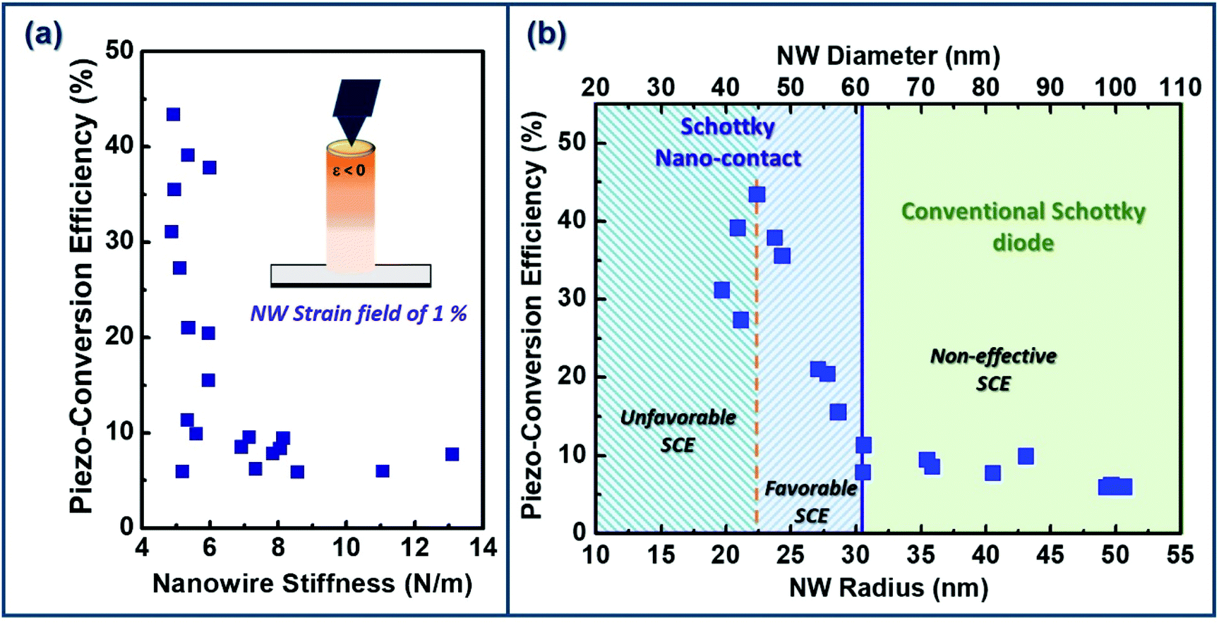 | ||
| Fig. 6 (a) Electromechanical coupling coefficient, η, variation as a function of the NW stiffness for a deformation of 1%. The variation in the 5.9–43.4% range highlights that the coupling coefficient is not only driven by the NW mechanical characteristics. (b) Variation of η as a function of the NW radius. The OV can also be affected both by the behaviour of the Schottky diode harvesting the generated OV, and by the influence of the surface charge effects (SCE). | ||
Influence of the Schottky diode nano-contact
The Schottky diode through which are collected the piezo-generated charges, and in particular its size, can significantly affect the OV harvesting21 (Fig. 7a): when the radius of the diode is lower than the depletion width (fixed by the doping) in NWs, the conventional description of the Schottky diode cannot be applied. The description of the Schottky nano-contact must be considered,21 where the effective Schottky barrier height, ΦSchottkyB, becomes a function of the diode size.59,60 The smaller is the diode size, the lower is the barrier height and the more important is the tunneling effect. This gives rise to a better energy harvesting and then to a highest electromechanical efficiency. In the present work, the Schottky diode is directly deposited on the top of each individual NW (Fig. 2). The diode size is thus fixed by the NW diameter. Plotting of the electromechanical coupling as a function of the NW radius (Fig. 6b) unambiguously evidences a strong relation between these two parameters (we remember here that each considered NW is characterized by a degree of compression of 1%): for radius higher than 30 nm, the OV is almost constant indicating its harvesting through a classical Schottky diode. By contrast, for smaller radii, the coupling efficiency strongly increases demonstrating that the OV is harvested through a Schottky nano-contact. The boundary between these two regimes points to a depletion width in our NWs of ∼30 nm.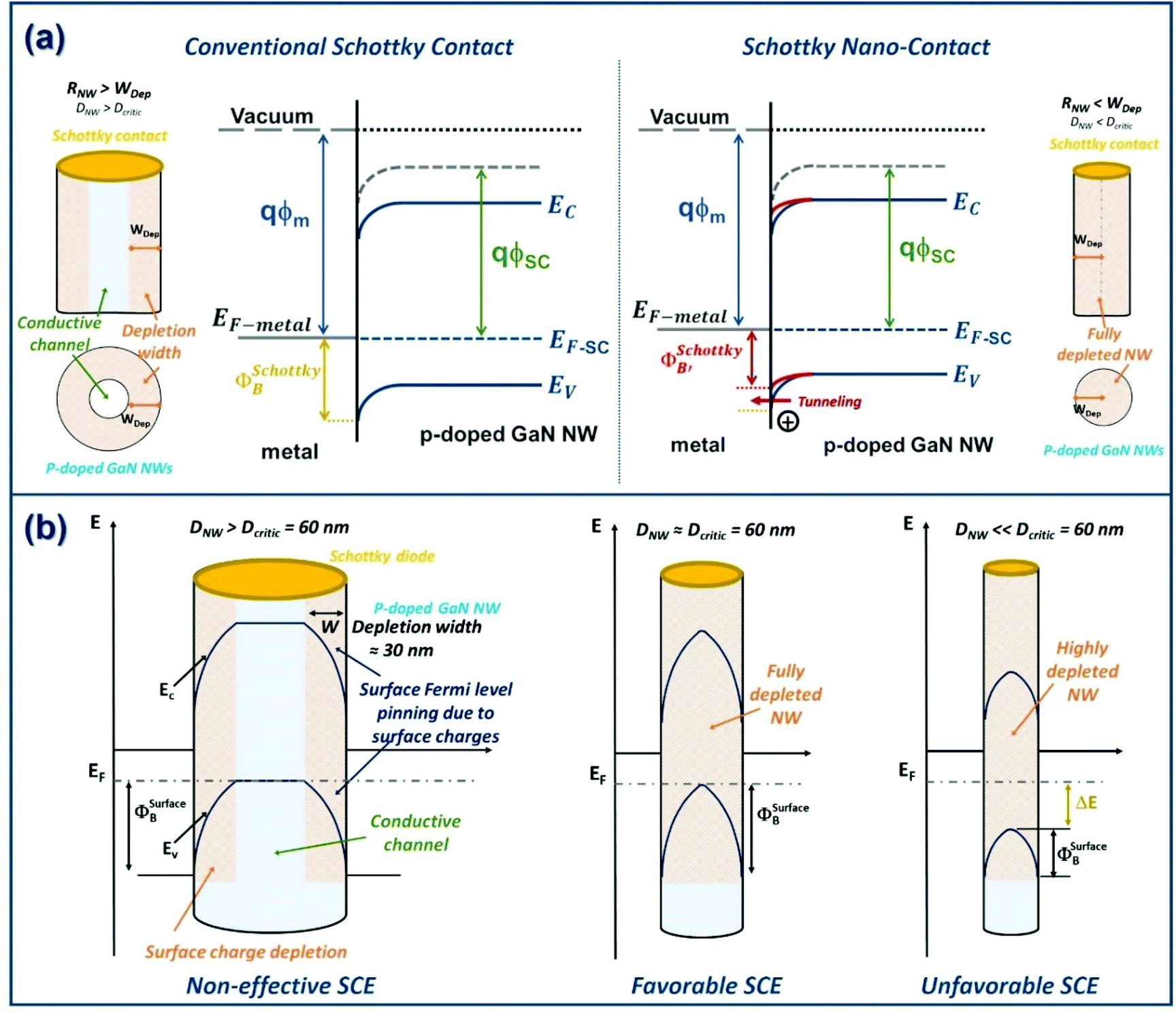 | ||
| Fig. 7 (a) Band diagrams of the interface between the GaN NW and the top metallic deposition playing the role of the Schottky diode. When the radius of the NW is larger than the depletion width (30 nm estimated in our NWs), the conventional description of the Schottky diode is considered. The Schottky barrier, ΦSchottkyB, is directly related to the band bending. By contrast, for NW radius smaller than the depletion width, the diode is governed by its nanometer size. The effective Schottky barrier is thus lowered with ΦSchottkyB′ < ΦSchottkyB, which gives rise to an enhanced harvesting of the OV and thus an enhanced electromechanical coupling coefficient. (b) Schematic representation of the Fermi level pinning in p-doped GaN NWs with different diameters, where ΦSurfaceB is the maximal surface barrier height and ΔE is the energy difference between the Fermi level and the valence band minimum. For NW radius larger than the depletion width, the SCE do not affect the piezo-generation. By contrast, for NW radius around 22–30 nm, the NW is fully depleted and SCE become favourable for piezo-conversion. However, when the NW radius becomes smaller than 22 nm, SCE turn out to be unfavourable. ΦSurfaceB is decreased, leading to an increase of the NW resistivity and thus to a degradation of the piezo-response. | ||
Influence of the surface charge effects (SCE)
The SCE, strongly pronounced in GaN NWs,38 give rise to surface Fermi level pinning (SFLP) inducing the formation of a depletion region along the NW edge with a width fixed by the NW doping.61 Depending on the NW diameter, the SFLP leads to a partial/complete depletion19,20 of the NW volume. This induces an effective reduction of the free carrier concentration, known to be detrimental to the piezo-response due to their screening of the piezoelectric charges. The OV generation and therefore the coupling efficiency (Fig. 7b) are thus affected. For NW radius, RNW, larger than the depletion width (30 nm estimated in our NWs), the depletion zone surrounds a conduction channel. The existence of this conductive NW core implies that the SCE do not affect the free carrier concentration and thus the piezo-conversion, η remaining approximatively constant. By contrast, when RNW is comparable to the depletion width, the NW is fully depleted with a surface barrier height, ΦSurfaceB, of the order of the SFLP. The free carrier density and thus the screening effect are reduced,19,20 enhancing the OV, which reach up to 43.4% for radii in the 22–30 nm range. In these conditions, the SCE are favorable for piezo-conversion. However, when RNW becomes really small, SCE turn out to be unfavorable. ΦSurfaceB is decreased and the carrier density reduction is so important that the NW becomes highly resistive, thereby limiting also the piezo-charge circulation with the external electrical circuit. The piezo-response is degraded, as observed for RNW smaller than 22 nm. These results experimentally illustrate the SCE influence, until to now theoretically predicted,19,20,32 on the piezo-conversion capacity of single GaN NWs.Conclusion
By using a unique advanced nano-characterization tool derived from AFM to probe the piezoelectric response of GaN NWs axially compressed with a well-controlled applied force, we have directly correlated the output signal generation of NWs with their mechanical characteristics and especially their stiffness. In this way, we were able to experimentally highlight the intrinsic link existing between the degree and the mode of deformation of the GaN NWs and their piezo-response. Thus, under axial compression, “rigid” NWs (k ≥ 5 Nm−1 or δ ≤ 3.5 GPa) are purely compressed and the generated OV is proportional to the degree of compression. By contrast, for “flexible” NWs, (k < 5 Nm−1 or δ > 3.5 GPa), a deformation combining axial compression and a slight buckling of the NW body is assumed. The OV is thus affected by the degree of compression and buckling. In the extreme case (high applied force and very flexible nanostructure), the buckling becomes bending and leads to a degradation of the generated OV.With this technique, we have also quantified the electromechanical coupling coefficient of GaN NWs (NWs with a stiffness ≥5 Nm−1 (elastic modulus ≤3.5 GPa)), a required and crucial figure of merit to discuss the real potential of NWs for developing piezoelectric devices. This coefficient can reach up to 43.4% in our GaN NWs. Thanks to the careful investigation of the results, we have pointed that the coupling coefficient (directly proportional to the OV) may not be affected only by the NW mechanical characteristics, but can be also linked to two other critical parameters. We have established that the coupling coefficient is affected by the formation of the Schottky nano-contact harvesting the piezo-generated energy when the NW radius is lower than 30 nm, corresponding to the depletion width in our GaN NWs. We have also experimentally demonstrated, for the first time, that the electromechanical coupling coefficient can be extremely sensitive to the surface charge effects, strongly pronounced in sub-100 nm wide GaN NWs. Thus, for NW radius higher than 30 nm, the SC have no effect on the piezo-conversion. By contrast, for lower radius, the expression of SCE is dominant: for radius around 22–30 nm, SCE become favorable for piezo-conversion due to advantageous screening effect of the free carrier into the fully depleted NWs; but for NW radius smaller than 22 nm, SCE turn out to be unfavourable and lead to a degradation of the piezo-conversion efficiency caused by the too important resistivity of the NWs.
Even though the present study has been established as part of AFM characterization, the applied axial compression as well as the NW configuration with the Schottky electrode directly deposited on the NW top, reflect the deformation and harvesting conditions experienced in real nanogenerator devices. Thus, these experimental establishments open new perspectives to improve the electromechanical coupling properties of the NW, a prerequisite for developing high efficient piezo-generators ready for technological transfer. For example, the integration of our slightly p-doped GaN NWs with homogeneous radius around 25 nm is a promising way.
Experimental
GaN NWs fabrication
GaN NWs were grown on Si(111)n+ substrates following the self-assembled free-catalyst methods by plasma-assisted molecular beam epitaxy (PA-MBE), active nitrogen being supplied by a radio-frequency plasma cell. The NW growth was performed at 760 °C under N-rich conditions with an N/Ga ratio of about 1.36. During the growth, the Mg cell was kept at 400 °C with the shutter closed in order to induce a p-type residual doping of GaN NWs. Prior to the growth of GaN NWs, a 2.5 nm-thick AlN buffer layer was deposited, allowing for a better control of the NW nucleation, density and orientation.62–64 This AlN interlayer presents a conductive character as explained in previous reported works.27,39,46 The GaN NWs formed under these growth conditions are vertically aligned with hexagonal shape delimited by {10–10} planes65 and present a Nitrogen polarity.66 They are characterized by a height of 1050 ± 200 nm, a diameter of 50 ± 30 nm and a density of 8 × 10⁸ NW cm−2.Sample preparation for characterization by AFM-Resiscope
The GaN NWs with their by sub-100 nm wide diameters are characterized by a strong flexibility.27 To circumvent this problem of high-flexibility inducing possible leakage of the piezoelectric charges and instability of the AFM tip/NW contact,21 the mechanical resistance of the NWs was increased by partially embedding their base into a polymethyl methacrylate (PMMA) resist layer. The PMMA was spin coated on the sample surface after the NW growth and etch-back by using reactive ion etching (RIE) with oxygen plasma to uncover the top portion of the NWs. Then, a diluted-HF etching was performed in order to remove the Ga2O3 oxide layer formed on the NWs top during the plasma treatment. For the set of piezoelectric conversion measurements, the GaN NWs emerging from the PMMA are characterized by a height equal to 200 ± 200 nm, the diameter remaining unchanged. By combining the NW and resist height measurements, performed by combining AFM and SEM characterization, we have estimated the resist height to ∼850 nm.In order to ensure reliable measurements of the piezo-generated energy and circumvent a potential and non-controllable degradation of the contact, we have directly deposited the diode on the NW top. After a wet etching step to remove residual oxide present at the NW top, we have deposited by electron beam evaporation a thin 5nm-Cr/20 nm-Pt top metallic film playing the role of collecting electrode. For this step, the NW sample was normally oriented regarding the metallic charges to ensure a deposition localized at the NW top and not covering the NW sidewalls. Thus, in these conditions, a pure metal/metal contact is formed between the AFM tip and the NWs, leading to a more efficient contact and thus energy harvesting under fast AFM scanning conditions.
Conflicts of interest
There are no conflicts to declare.Acknowledgements
This work was financially supported by the the French National Research Agency through the GANEX program (ANR-11-LABX-0014), the Project SCENIC (ANR-20-CE09-0005) and as part of the “Investissements d'Avenir” program (reference: ANR-10-LABX-0035, Labex NanoSaclay). The results in this paper also partly come from the EMPIR 19ENG05 NanoWires. This project has received funding from the EMPIR programme co-financed by the Participating States and from the European Union's Horizon 2020 research and innovation programme” Finally, the work was also partly supported by the French Renatech/Renatch + networks.References
- K. Tomioka, M. Yoshimura and T. A. Fukui, Nature, 2012, 488, 189 CrossRef CAS PubMed.
- S. Gazibegovic, D. Car, H. Zhang, S. C. Balk, J. A. Logan, M. W. A. de Moor, M. C. Cassidy, R. Schmits, D. Xu, G. Wang, P. Krogstrup, R. L. M. Op het Veld, K. Zuo, Y. Vos, J. Shen, D. Bouman, B. Shojaei, D. Pennachio, J. S. Lee, P. J. van Veldhoven, S. Koelling, M. A. Verheijen, L. P. Kouwenhoven, C. J. Palmstrøm and E. P. A. M. Bakkers, Nature, 2017, 548, 434 CrossRef CAS PubMed.
- J. Wang, M. S. Gudiksen, X. Duan, Y. Cui and C. M. Lieber, Science, 2001, 24, 1455 CrossRef PubMed.
- M. Karimi, M. Heurlin, S. Limpert, V. Jain, X. Zeng, I. Geijselaers, A. Nowzari, Y. Fu, L. Samuelson, H. Linke, M. T. Borgström and H. Pettersson, Nano Lett., 2018, 18, 365 CrossRef CAS PubMed.
- L. Xu, Z. Dai, G. Duan, L. Guo, Y. Wang, H. Zhou, Y. Liu, W. Cai, Y. Wang and T. Li, Sci. Rep., 2015, 5, 10507 CrossRef PubMed.
- Z. Chen, Z. Wang, X. Li, Y. Lin, N. Luo, M. Long, N. Zhao and J.-B. Xu, ACS Nano, 2017, 11, 4507 CrossRef CAS PubMed.
- A. E. Kacimi, E. Pauliac-Vaujour, O. Delléa and J. Eymery, Nanomaterials, 2018, 8, 426 CrossRef PubMed.
- X. Zhang, J. Villafuerte, V. Consonni, J.-F. Capsal, P.-J. Cottinet, L. Petit and M.-Q. Le, Nanomaterials, 2021, 11, 1712 CrossRef CAS PubMed.
- Y. Geng, A. Bin Che Mahzan, K. Jeronimo Martinez, M. M. Saleem, P. Lomax, E. Mastropaolo and R. Cheung, Nanotechnology, 2021, 17, 32 Search PubMed.
- S. Duan, J. Wu, J. Xia and W. Lei, Sensors, 2020, 20, 2820 CrossRef CAS PubMed.
- S. Xu, Y. Qin, C. Xu, Y. Wei, R. Yang and Z. L. Wang, Nat. Nanotechnol., 2010, 5, 366 CrossRef CAS PubMed.
- G. Liu, S. Zhao, R. D. E. Henderson, Z. Leonenko, E. Abdel-Rahman, Z. Mi and D. Ban, Nanoscale, 2016, 8, 2097 RSC.
- D.-M. Shin, H. J. Han, W.-G. Kim, E. Kim, C. Kim, S. W. Hong, H. K. Kim, J.-W. Oh and Y.-H. Hwang, Energy Environ. Sci., 2015, 8, 3198 RSC.
- M. Ani Melfa Roji, G. Jiji and T. Ajith Bosco Raj, RSC Adv., 2017, 7, 33642 RSC.
- X. Cao, Y. Xiong, J. Sun, X. Zhu, Q. Sun and Z. L. Wang, Adv. Funct. Mater., 2021, 31, 2102983 CrossRef CAS.
- M. Minary-Jolandan, R. A. Bernal, I. Kuljanishvili, V. Parpoil and H. D. Espinosa, Nano Lett., 2012, 12, 970 CrossRef CAS PubMed.
- M. H. Zhao, Z. L. Wang and S. X. Mao, Nano Lett., 2004, 4, 587 CrossRef CAS.
- R. Agrawal and H. D. Espinosa, Nano Lett., 2011, 11, 786 CrossRef CAS PubMed.
- H.-Y. Chen, R.-S. Chen, F.-C. Chang, L.-C. Chen, K.-H. Chen and Y.-J. Yang, Appl. Phys. Lett., 2009, 95, 143123 CrossRef.
- R. Calarco, T. Stoica, O. Brandt and L. Geelhaar, J. Mater. Res., 2011, 26, 2157 CrossRef CAS.
- N. Jamond, P. Chrétien, L. Gatilova, E. Galopin, L. Travers, J.-C. Harmand, F. Glas, F. Houzé and N. Gogneau, Nanoscale, 2017, 9, 4610 RSC.
- M. Sharma, V. Srinivas, G. Madras and S. Bose, RSC Adv., 2016, 6, 6251 RSC.
- Z. L. Wang and J. Song, Science, 2006, 312, 242 CrossRef CAS PubMed.
- Y. F. Lin, J. Song, Y. Ding, S.-Y. Lu and Z. L. Wang, Appl. Phys. Lett., 2008, 92, 022105 CrossRef.
- Y. S. Zhou, K. Wang, W. Han, S. C. Rai, Y. Zhang, Y. Ding, C. Pan, F. Zhang, W. Zhou and Z. L. Wang, ACS Nano, 2012, 6, 6478 CrossRef CAS PubMed.
- C.-Y. Chen, T.-H. Liu, Y. Zhou, Y. Zhang, Y.-L. Chueh, Y.-H. Chu Jr., H. He and Z. L. Wang, Nano Energy, 2012, 1, 424 CrossRef CAS.
- N. Gogneau, P. Chrétien, E. Galopin, S. Guilet, L. Travers, J.-C. Harmand and F. Houzé, Phys. Status Solidi RRL, 2014, 8, 414 CrossRef CAS.
- X. Li, D. Xiao, H. Zheng, X. Wei, X. Wang, L. Gu, Y.-S. Hu, T. Yang and Q. Chen, Nano Energy, 2016, 20, 194 CrossRef CAS.
- K. Zheng, Z. Zhang, Y. Hu, P. Chen, W. Lu, J. Drennan, X. Han and J. Zou, Nano Lett., 2016, 16, 1787 CrossRef CAS PubMed.
- S. Yang, L. Wang, X. Tian, Z. Xu, W. Wang, X. Bai and E. Wang, Adv. Mater., 2012, 24, 4676 CrossRef CAS PubMed.
- Z. Wang, J. Hu, A. P. Suryavanshi, K. Yum and M.-F. Yu, Nano Lett., 2007, 7, 2966 CrossRef CAS PubMed.
- R. Tao, M. Mouis and G. Ardila, Adv. Electron. Mater., 2018, 4, 1700299 CrossRef.
- P. G. Kang, T. K. Lee, C. W. Ahn, I. W. Kim, H. H. Lee, S. B. Choi and J. H. Jung, Nano Energy, 2015, 17, 261 CrossRef CAS.
- P. A. Alekseev, V. A. Sharov, P. Geydt, M. S. Dunaevskiy, V. V. Lysak, G. E. Cirlin, R. R. Reznik, A. I. Khrebtov, I. P. Soshnikov and E. Lähderanta, Phys. Status Solidi RRL, 2017, 12, 1700358 CrossRef.
- P. X. Gao, J. Song, J. L. Liu and Z. L. Wang, Adv. Mater., 2007, 19, 67 CrossRef CAS.
- M.-P. Lu, J. Song, M.-Y. Lu, M.-T. Chen, Y. Gao, L.-J. Chen and Z. L. Wang, Nano Lett., 2009, 9, 1223 CrossRef CAS PubMed.
- T. K. Sodhi, P. Chretien, F. Houzé, N. Gogneau, et al. To be submitted.
- C. G. Van de Walle and D. Segev, J. Appl. Phys., 2007, 101, 081704 CrossRef.
- G. Jacopin, A. De Luna Bugallo, L. Rigutti, P. Lavenus, F. H. Julien, Y.-T. Lin, L.-W. Tu and M. Tchernycheva, Appl. Phys. Lett., 2014, 104, 023116 CrossRef.
- J. Liu, P. Fei, J. Song, X. Wang, C. Lao, R. Tummala and Z. L. Wang, Nano Lett., 2008, 8, 328 CrossRef CAS PubMed.
- N. Gogneau, N. Jamond, P. Chrétien, F. Houzé, E. Lefeuvre and M. Tchernycheva, Semicond. Sci. Technol., 2016, 31, 103002 CrossRef.
- X. Xu, A. Potié, R. Songmuang, J. W. Lee, B. Bercu, T. Baron, B. Salem and L. Montès, Nanotechnology, 2011, 22, 105704 CrossRef PubMed.
- A. Vecchiola, P. Chrétien, S. Delprat, K. Bouzehouane, O. Schneegans, P. Seneor, R. Mattana, S. Tatay, B. Geffroy, Y. Bonnassieux, D. Mencaraglia and F. Houzé, Appl. Phys. Lett., 2016, 108, 243101 CrossRef.
- O. Schneegans, P. Chretien and F. Houze, French patent, FR 1001940, 2010; O. Schneegans, P. Chretien and F. Houze, International PCT, WO2011/138738, 2011.
- B. Pérez-García, J. Zúñiga-Pérez, V. Muñoz-Sanjosé, J. Colchero and E. Palacios-Lidón, Nano Lett., 2007, 7, 1505 CrossRef PubMed.
- N. Jamond, P. Chrétien, F. Houzé, L. Lu, L. Largeau, O. Maugain, L. Travers, J.-C. Harmand, F. Glas, E. Lefeuvre, M. Tchernycheva and N. Gogneau, Nanotechnology, 2016, 27, 325403 CrossRef CAS PubMed.
- Y. Gao and Z. L. Wang, Nano Lett., 2007, 7, 2499 CrossRef CAS PubMed.
- Z. Wang, X. Zu, L. Yang, F. Gao and W. J. Weber, Phys. E, 2008, 40, 561 CrossRef CAS.
- F.-C. Hsu and T.-C. Chen, AIMS Mater. Sci., 2019, 6, 377 CAS.
- J. Wang, Z. Zeng, C. R. Weinberger, Z. Zhang, T. Zhu and S. X. Mao, Nat. Mater., 2015, 14, 594 CrossRef CAS PubMed.
- H. S. Park, K. Gall and J. A. Zimmerman, J. Mech. Phys. Solids, 2006, 54, 1862 CrossRef CAS.
- C. Y. Tang, L. C. Zhang and K. Mylvaganam, Comput. Mater. Sci., 2012, 51, 117 CrossRef CAS.
- W.-J. Lee, J.-G. Chang, S.-P. Ju, M.-H. Weng and C.-H. Lee, Nanoscale Res. Lett., 2011, 6, 352 CrossRef PubMed.
- N. Gogneau, P. Chrétien, E. Galopin, S. Guilet, L. Travers, J.-C. Harmand and F. Houzé, Appl. Phys. Lett., 2014, 104, 213105 CrossRef.
- M.-Y. Lu, J. Song, M.-P. Lu, L.-J. Lee and Z. L. Wang, ACS Nano, 2009, 3, 357 CrossRef CAS PubMed.
- Y. F. Lin, J. Song, Y. Ding, S.-Y. Lu and Z. L. Wang, Appl. Phys. Lett., 2008, 92, 022105 CrossRef.
- Y. S. Zhou, W. Han, S. C. Rai, Y. Zhang, Y. Ding, C. Pan, F. Zhang, W. Zhou and Z. L. Wang, ACS Nano, 2012, 6, 6478 CrossRef CAS PubMed.
- T.-C. Hou, Y. Yang, Z.-H. Lin, Y. Ding, C. Park, K. C. Pradel, L.-J. Chen and Z. L. Wang, Nano Energy, 2013, 2, 387 CrossRef CAS.
- G. D. J. Smit, S. Rogge and T. M. Klapwijk, Appl. Phys. Lett., 2002, 81, 3852 CrossRef CAS.
- G. D. J. Smit, S. Rogge and T. M. Klapwijk, Appl. Phys. Lett., 2002, 80, 2568 CrossRef CAS.
- L. Polenta, M. Rossi, A. Cavallini, R. Calarco, M. Marso, R. Meijers, T. Richter, T. Stoica and H. Lüth, ACS Nano, 2008, 2, 287 CrossRef CAS PubMed.
- M. D. Brubaker, I. Levin, A. V. Davydov, D. M. Rourke, N. A. Sanford, V. M. Bright and K. A. Bertness, J. Appl. Phys., 2011, 110, 053506 CrossRef.
- R. Songmuang, O. Landré and B. Daudin, Appl. Phys. Lett., 2007, 91, 251902 CrossRef.
- K. A. Bertness, A. Roshko, L. M. Mansfield, T. E. Harvey and N. A. Sanford, J. Cryst. Growth, 2007, 300, 94 CrossRef CAS.
- L. Largeau, D. L. Dheeraj, M. Tchernycheva, G. E. Cirlin and J.-C. Harmand, Nanotechnology, 2008, 19, 155704 CrossRef CAS PubMed.
- L. Largeau, E. Galopin, N. Gogneau, L. Travers, F. Glas and J.-C. Harmand, Cryst. Growth Des., 2012, 12, 2724 CrossRef CAS.
Footnote |
| † Electronic supplementary information (ESI) available. See DOI: 10.1039/d1nr07863a |
| This journal is © The Royal Society of Chemistry 2022 |