
Oxygen-induced degradation in AgBiS2 nanocrystal solar cells†
David
Becker-Koch
 a,
Miguel
Albaladejo-Siguan
a,
Joshua
Kress
a,
Rhea
Kumar
b,
Yvonne J.
Hofstetter
a,
Qingzhi
An
a,
Artem A.
Bakulin
b,
Fabian
Paulus
a and
Yana
Vaynzof
*a
a,
Miguel
Albaladejo-Siguan
a,
Joshua
Kress
a,
Rhea
Kumar
b,
Yvonne J.
Hofstetter
a,
Qingzhi
An
a,
Artem A.
Bakulin
b,
Fabian
Paulus
a and
Yana
Vaynzof
*a
aIntegrated Center for Applied Physics and Photonic Materials and Center for Advancing Electronics Dresden, Nöthnitzer Str. 61, 01187 Dresden, Germany. E-mail: yana.vaynzof@tu-dresden.de
bDepartment of Chemistry and Centre for Processible Electronics, Imperial College London, London W120BZ, UK
First published on 14th December 2021
Abstract
AgBiS2 nanocrystal solar cells are among the most sustainable emerging photovoltaic technologies. Their environmentally-friendly composition and low energy consumption during fabrication make them particularly attractive for future applications. However, much remains unknown about the stability of these devices, in particular under operational conditions. In this study, we explore the effects of oxygen and light on the stability of AgBiS2 nanocrystal solar cells and identify its dependence on the charge extraction layers. Normally, the rate of oxygen-induced degradation of nanocrystals is related to their ligands, which determine the access sites by steric hindrance. We demonstrate that the ligands, commonly used in AgBiS2 solar cells, also play a crucial chemical role in the oxidation process. Specifically, we show that the tetramethylammonium iodide ligands enable their oxidation, leading to the formation of bismuth oxide and silver sulphide. Additionally, the rate of oxidation is impacted by the presence of water, often present at the surface of the ZnO electron extraction layer. Moreover, the degradation of the organic hole extraction layer also impacts the overall device stability and the materials’ photophysics. The understanding of these degradation processes is necessary for the development of mitigation strategies for future generations of more stable AgBiS2 nanocrystal solar cells.
 Yana Vaynzof | Prof. Dr Yana Vaynzof is the Chair for Emerging Electronic Technologies at the Technical University of Dresden (Germany). Prior to commencing her current position in 2019, Yana was a postdoctoral research associate at the Cavendish Laboratory, Cambridge (UK) and an assistant professor at Heidelberg University (Germany). Yana Vaynzof is the recipient of a number of fellowships and awards, including the ERC Starting Grant, Gordon Wu Fellowship, Henry Kressel Fellowship, Fulbright-Cottrell Award and the Walter Kalkhof-Rose Memorial Prize. Her research interests lie in the field of emerging photovoltaics focusing on the study of material and device physics of organic, quantum dot and perovskite solar cells. |
Introduction
Nanocrystal (NC) or quantum dot (QD) photovoltaic diodes (PVs) have made enormous strides in recent years, with significant enhancement in their record power conversion efficiency (PCE).1 The use of NCs, rather than the bulk material, is motivated by the ability to tune their optoelectronic properties by controlling the size, shape and ligands of the NCs.2 Additionally, the properties of the NCs can be optimized according to the requirements imposed by the other layers of the photovoltaic device.3,4 While significant research efforts have been dedicated to improving both the efficiency and stability of NC PVs,5–7 the most efficient devices are often based on lead-containing QDs, such as lead sulphide (PbS) or lead halide perovskites, raising significant concerns regarding the environmental impact and sustainability of this technology.8–11 A much more environmentally-friendly alternative to these compositions are the silver bismuth disulphide (AgBiS2) NC PVs that were first introduced by Bernechea et al. in 2016.12 Since then, the majority of scientific efforts have been dedicated to improving the synthesis and device performance optimisation of AgBiS2 NCs. For example, it has been shown that the addition of amines during the synthesis improves the optoelectronic properties of the crystals and their performance in the device.13 Similarly, attention has been devoted to optimising the ligand exchange procedure, which can be performed either in a layer-by-layer fashion12,14 or via a liquid phase exchange.15,16 Alternatively, it has been shown that the ligand exchange step can be omitted by directly synthesising the nanocrystals with the final ligands.17 While these efforts are very important for further improving the performance of AgBiS2 PVs, very little is known about the stability of these devices.18 In particular, only the shelf stability of AgBiS2 NC PVs in the dark has been reported thus far.12,19,20 It has also been shown that AgBiS2 NC PVs maintain their performance upon a one-time exposure to water,19 however their operational stability under continuous illumination was not yet examined.Herein, we investigate the evolution of the photovoltaic performance of AgBiS2 NC PVs with tetramethylammonium iodide (TMAI) as ligand under operational conditions upon exposure to different environments. In particular, we focus on understanding the influence of exposure to oxygen and the role of extraction layers on the performance evolution of the device. For this purpose, we investigate devices with two different hole transport layers (HTLs), namely poly[[4,8-bis[(2-ethylhexyl)oxy]benzo[1,2-b:4,5-b′]dithiophene-2,6-diyl][3-fluoro-2-[(2-ethylhexyl)carbonyl]thieno[3,4-b]thiophenediyl]] (PTB7)/molybdenum trioxide (MoO3) and poly-[bis-(4-phenyl)-(2,4,6-trimethylphenyl)-amine] (PTAA) doped with C60F48 (labelled in the following as PTAA:C60F48), and two different deposition methods for the ZnO electron transport layer (ETL) – either via a sol–gel route or via the deposition of ZnO nano-particles. The four possible device configurations alongside with the molecular structure of the used materials are summarised in Fig. 1. By employing a range of spectroscopic and microscopic techniques, we identify the degradation mechanisms of AgBiS2 NC PVs and their impact on the device photophysics.
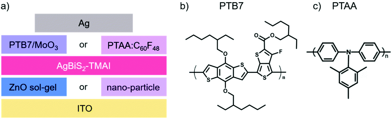 | ||
| Fig. 1 Structure of devices and materials. (a) Architecture of the studied solar cells. The HTL consists either of PTB7/MoO3 or PTAA:C60F48 and the molecular structure is shown in (b) and (c) for the polymers, respectively. The ETL was made from ZnO but either in a sol–gel thin film or as nano-particles, resulting in overall four combinations which were examined. | ||
Results and discussion
Photovoltaic performance and stability
Our choice of extraction layers was motivated by the fact that these are the most commonly used extraction layers in AgBiS2 PVs.12,14,20 We find that irrespective of the choice of HTL, the use of ZnO nano-particles (np) results in an increased short-circuit current (JSC), due to the improved charge extraction through the larger surface area of the ZnOnp layer (see Fig. S1†). PTB7/MoO3 was one of the first hole extraction layers used in AgBiS2 PVs and remains the most common choice to date.14 Recently, we introduced a doped PTAA:C60F48 as HTL in both PbS QD and AgBiS2 NC PVs,21 which due to its efficacious electron blocking leads to an improvement in device performance as compared to PTB7/MoO3. The best performing devices are those which combine ZnOnp with PTAA:C60F48 (see Fig. S1†), however, as will be shown later, high initial photovoltaic performance does not guarantee good device stability. The other three device configurations lead to a similar device performance.The operational stability of the devices was examined by continuously tracking their performance under 1 sun illumination and exposure to dry air (80% nitrogen, 20% oxygen, <15 ppmV relative humidity, temperature ∼35 °C). The evolution of the photovoltaic parameters of these devices is displayed in Fig. 2. While an identical AgBiS2 NC active layer was used in combination with different charge extraction layers, it is evident that the operational stability of the devices is starkly different. The most stable devices are achieved with the combination of ZnOsg and PTAA:C60F48. The open circuit voltage (VOC) and the fill factor (FF) remain largely unchanged, while the JSC is slowly declining, leading to a gradual reduction in PCE. Interestingly, devices with the same organic extraction layer, but with ZnOnp as ETL exhibit a rapid performance loss, especially in the first few hours of operation. The most prominent decrease is observed in the JSC, but also the VOC and FF are reduced. The loss in performance is still less pronounced than in devices with PTB7/MoO3 as HTL, which independent of the ETL lose all photovoltaic performance within 24 h. This occurs on a faster time scale for the device based on ZnOnp, rather than ZnOsg – again suggesting that the latter is beneficial for device stability. Another interesting observation is that devices based on ZnOsg and PTAA:C60F48 exhibit an initial increase in performance in the first few hours of operation. This is very similar to what is commonly observed in PbS QD solar cells, which increase their performance under oxygen exposure as well.22–25 This increase is typically associated with the passivation of trap states at the surface of the NCs, which positively impacts their recombination dynamics. A similar process is also likely to occur in the case of AgBiS2 NCs. Indeed, light-intensity-dependent VOC measurements confirmed, that exposure to oxygen increases the slope of VOCvs. light intensity from 1.3 kT q−1 to 1.4 kT q−1 and 2.0 kT q−1 after 2.5 h and 24 h, respectively (Fig. S2†). In PbS QDs this was linked to the formation of a beneficial thin shell of oxidised species around the dots,25 which is likely to also be the case here. A similar process probably occurs also for the other three types of devices, but their degradation is so rapid that their performance evolution is dominated by other processes, which will be explored in detail in the following.
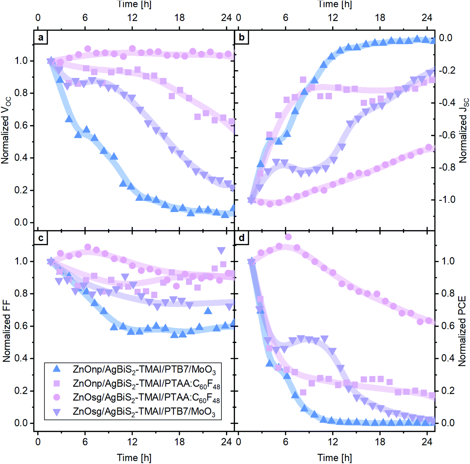 | ||
| Fig. 2 Photovoltaic evolution in dry air with continuous 1 sun illumination of AgBiS2 NC solar cells with different extraction layers. The photovoltaic parameters, (a) VOC, (b) JSC, (c) FF and (d) PCE, were averaged from several devices and normalized to their initial value. A guide for the eye in form of a line is added. | ||
Impact of degradation on device photophysics
To examine the impact of degradation on the photophysics of AgBiS2 NC films and devices, we applied transient absorption (TA) spectroscopy. In Fig. 3a and b TA spectra are compared for neat AgBiS2 NC films and films after degradation under O2 and light for 27.5 h (TA data for intermediate degradation times can be found in Fig. S3†). 700 nm pump pulses were used to excite above the AgBiS2 band gap. All spectra contain a broad photoinduced absorption (PIA) that spans the probing region. The spectra show modest changes (redshift) with time. The amplitude of the signal contains two components. A ∼100 ps short-lived component, which dominates the decay, we associate with mobile carriers and their bimolecular recombination. This is confirmed by flux-dependent TA measurements (Fig. S4†). The long-lived component that remains after 1 ns, extends beyond the 6 ns timescale of the measurement. As this component does not show pronounced dependence on the excitation flux, we attribute it to immobile trapped carriers.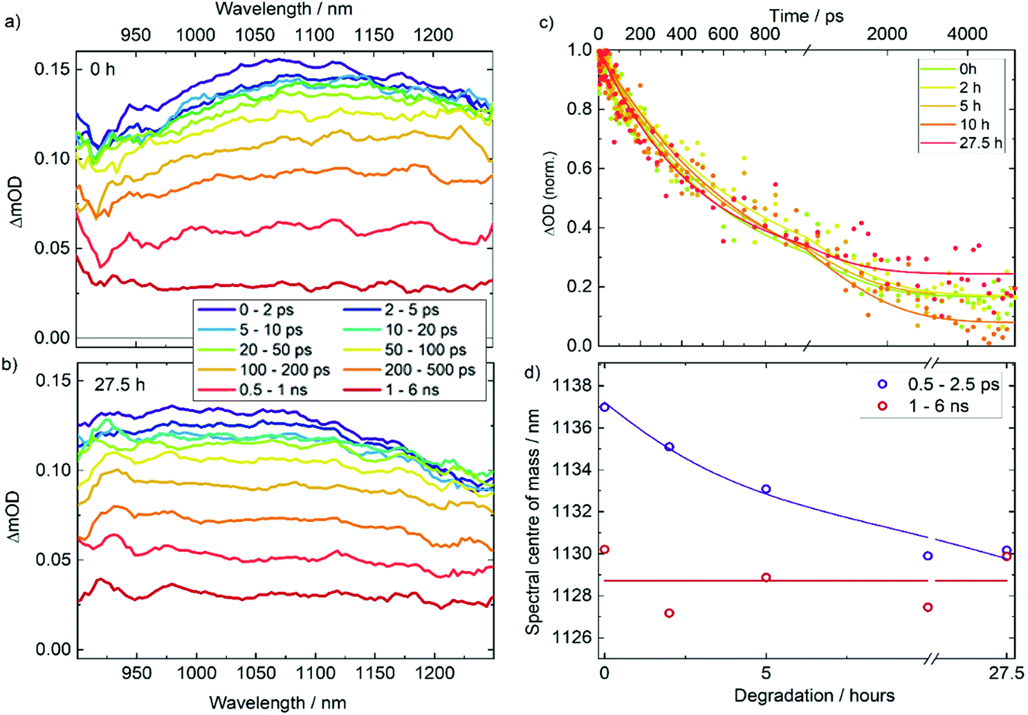 | ||
| Fig. 3 Transient absorption spectra for neat AgBiS2 films after (a) 0 h and (b) 27.5 h degradation following a 700 nm excitation. (c) Evolution in time of the normalised TA PIA signal for all films. (d) Centre of mass of PIA signal as a function of degradation time for early and late pump–probe time delays. | ||
Fig. 3c compares the evolution of the PIA amplitude as a function of time for all films. There is no clear correlation between the early time kinetics of the decay and the extent of degradation, which is in agreement with relatively high stability of AgBiS2 films on their own as discussed later. However, there is a greater amplitude of long-lived states (present after 1 ns) for the films exposed to oxygen for the longest periods of time. The decay appears to plateau at 3 ns for this trace, but continues until 4–5 ns for the films degraded for shorter amounts of time. This confirms our assignment of long-lived states to trapped charges. Interestingly, the PIA signal in the TA spectra blue shifts in the case of the degraded samples. The effect is particularly pronounced in the early time data where both mobile and trapped carriers are present in the film, while at long time delays, when only trapped carriers are present, all of the spectra look similar. As the peak we analyse is an excited state absorption (and not a ground state bleach) signal, it cannot be associated with a thermal artefact or a dynamic stark shift. The shift is also unlikely to be associated with charge and energy transfer as these phenomena are expected to happen at much faster, sub-ps, times in nanocrystal solids. We therefore conclude the change of the peak shape is associated with the change in population over the density of states, specifically and most likely, charge trapping. Charge trapping can be quantified through calculating the centre of mass for the TA spectra, as shown in Fig. 3d. We therefore propose that the spectral position (blueshift) of the PIA can be used as measure of relative population of trapped states in the material.
We have also measured TA spectra measured on AgBiS2 solar cells with the four different combinations of hole and electron transport layers for pristine and degraded conditions. Fig. 4a presents an example of the measurements while full data can be found in the ESI (Fig. S5†). The spectra have a generally similar shape for all device configurations, showing PIA features at the near-infrared (NIR) edge of the probing window and a ground state bleach at wavelengths approaching the visible region. However, the specific peak positions vary from sample to sample due to interference effects induced by the multilayer nature of the device and the contributions from the different hole extraction layers. Still, the TA spectra for all samples contain a long-lived component that remains after 6 ns, which generally reflects the broad and flat spectrum of trapped charges present at long time delays in the neat AgBiS2 film spectrum.
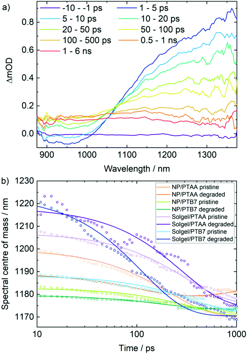 | ||
| Fig. 4 (a) TA spectrum for degraded nanoparticle ZnO/AgBiS2-TMAI/PTB7 device following a 700 nm pump excitation. (b) Centre of mass of PIA signal as a function of time for each device configuration. | ||
In order to characterise the effect of degradation on the charge dynamics in each device, the blue shift of the PIA in each device spectrum in Fig. 4a was quantified and interpreted as a representation of charge trapping. For each device, the spectral centre of mass across the PIA region was calculated at each timepoint and plotted as a function of time in Fig. 4b. The spectra of all devices were observed to blueshift from early times until 500 ps with a trace that was fitted to a monoexponential function.
As the blueshift is related to the population of trapped charges within the device, a shorter lifetime of this process illustrates faster charge trapping. Charge traps are formed as a consequence of degradation and hence each degraded device exhibits a faster timescale of charge trapping relative to the corresponding pristine device. In order to quantitatively describe the impact of degradation for each device configuration, the time constants for this process were extracted from the monoexponential fits. By calculating the percentage decrease of this lifetime for each degraded device relative to the corresponding pristine lifetime, we arrive at a metric that quantifies the effect of degradation on each device (Table 1). Hence from this analysis it is possible to quantitatively compare each device's susceptibility to degradation and, more specifically, the subsequent formation of active charge traps.
| Device | Blue shift time constant/ps | Decrease/% | |
|---|---|---|---|
| Pristine | Degraded | ||
| ZnOsg + PTAA:C60F48 | 306 | 281 | 8.2 |
| ZnOsg + PTB7/MoO3 | 356 | 109 | 69.4 |
| ZnOnp + PTAA:C60F48 | 210 | 114 | 45.7 |
| ZnOnp + PTB7/MoO3 | 366 | 178 | 51.4 |
In excellent agreement with the evolution of the photovoltaic performance, three of the four devices show a dramatically faster timescale of charge trapping as a result of degradation with approximately 45–70% increase in charge trapping upon degradation. The device that is the least affected by the degradation is the sol–gel ZnO/AgBiS2/PTAA:C60F48 device with only an 8% difference between pristine and degraded device charge trapping lifetimes, which is drastically lower than the other three device configurations. This suggests that the degradation products act as trapping sites that significantly impact the ability of the device to generate photocurrent.
Stability of AgBiS2 NCs
To examine the stability of the AgBiS2 NC active layers without the presence of different charge extraction layers, the NC films were prepared on glass or ITO for different spectroscopic measurements. The pristine state of these films after fabrication was compared to the state after being exposed for 17 to 24 h to dry air and 1 sun illumination. Fig. 5a displays X-ray photoemission spectroscopy (XPS) measurements of the Ag 3d, Bi 4f, S 2p, I 3d, C 1s and O 1s orbitals for both pristine and degraded films. We note that some oxygen can be detected in the pristine films, since their fabrication is conducted in ambient conditions. Fourier-transform infrared spectroscopy (FTIR) measurements confirm the complete exchange of the ligand from the NC synthesis, oleic acid (OA), with the ligand in the device, tetramethylammonium iodide (TMAI) (Fig. S6†), so the oxygen signal does not originate from OA, but from surface contamination. The carbon and iodine signals originate from the TMAI, as expected. Based on the atomic percentages of Ag, Bi and S (Table S1†), we calculate the ratios between those elements. The Ag/Bi ratio was 2.2, the S/Bi ratio was 1.4, resulting in an Ag/S ratio of 1.6, which represents a significant Ag excess in the NCs. We note that this is different to Bernechea et al. despite the fact that the same recipe and same precursor ratio were employed here during the synthesis. However, this result is consistent with the study by Öberg et al. which links a higher silver content to a better VOC and in tendency lower JSC, which might have limited the absolute performance in this study.26 A comparison between the pristine samples to the degraded ones reveals only small but significant changes in composition. The Ag 3d doublet does not change, neither in binding energy nor intensity. The overall oxygen amount increases, as does the carbon. The iodine signal is slightly reduced upon degradation, while the sulphur doublet at 161.5 eV and 162.2 eV remains largely unchanged. The strongest difference can be observed in the Bi 4f spectra, where the pristine doublet at 158.0 and 163.5 eV diminishes in comparison to the doublet associated with an oxidised bismuth species at 159.0 eV and 164.5 eV (see Fig. 5a[ii] and [vii]). These observations indicate an oxidation of the AgBiS2 NCs into Bi2O3.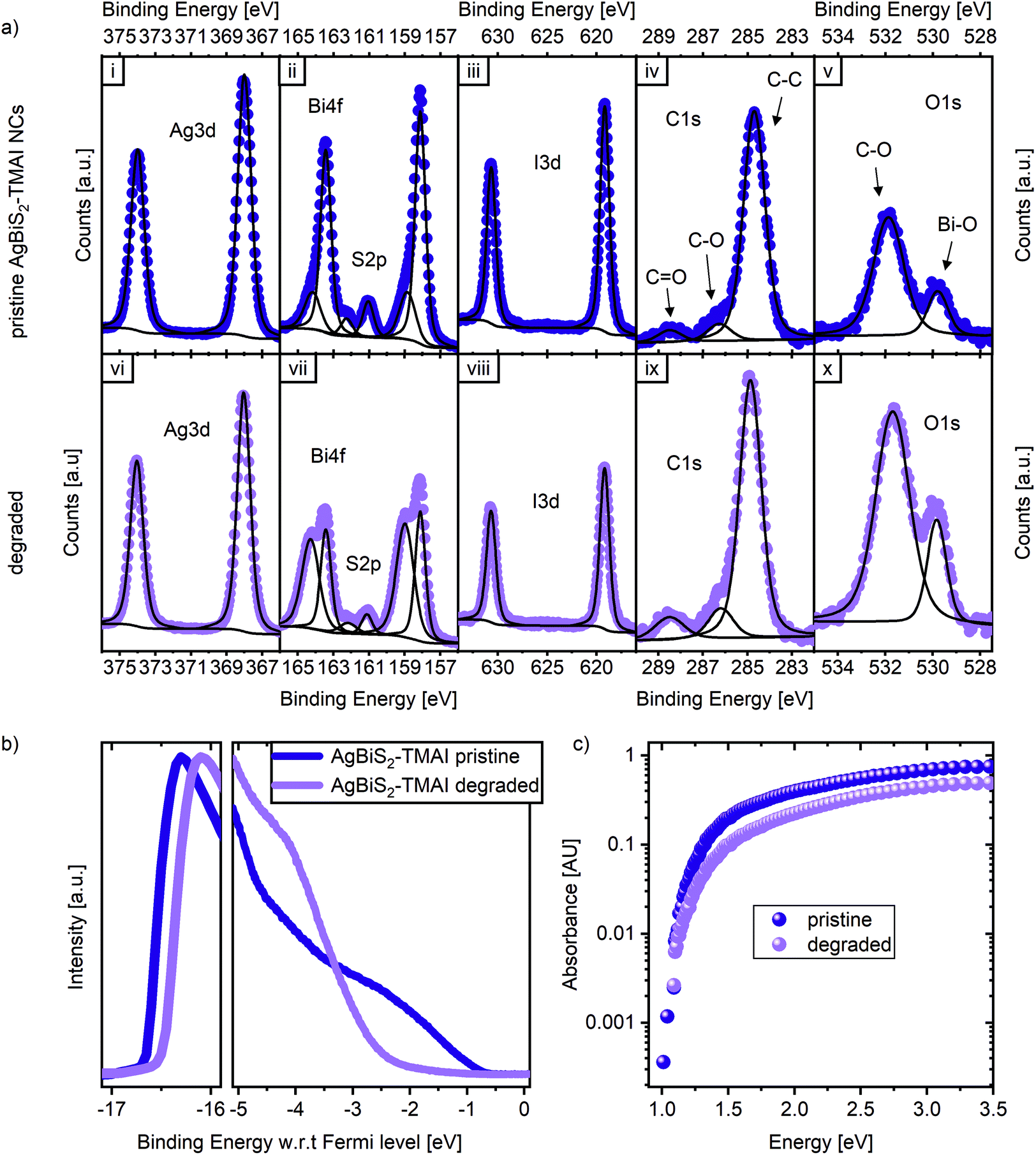 | ||
| Fig. 5 The degradation of AgBiS2-TMAI NCs. (a) XPS data of a pristine film in the top row, bottom row presents the state after 24 h of dry air and sunlight exposure. The scale is arbitrary but the same for each orbital. (b) UPS data for a pristine and 17 h degraded AgBiS2-TMAI film on ITO. (c) PDS measurement of the absorption of a pristine and 24 h degraded film. | ||
The formation of an oxide is also supported by ultra-violet photoemission (UPS) spectroscopy measurements shown in Fig. 5b. After degradation, the valence band onset strongly resembles the onset typical of a metal oxide with a large energetic offset of the valence band from the Fermi level.27,28 While this change observed in the UPS data might appear quite dramatic, it is important to remember that UPS probes only the top 1–2 nm of a film. This, together with the XPS results suggests, that while the very top surface of the layer has fully degraded to form Bi2O3, below the surface the NCs are mostly intact. This is supported by the presence of the low binding energy doublet in the XPS Bi 4f spectra of degraded samples, that can be observed due to the higher probing depth of XPS (∼10 nm). Additionally, X-ray diffraction patterns (XRD) of pristine and degraded AgBiS2 NC films show no structural degradation in the examined time frame (Fig. S7†). Moreover, photothermal deflection spectroscopy (PDS) measurements reveal that the absorption spectra (Fig. 5c), which are dominated by the bulk of the film, show relatively small changes upon degradation. Degraded films show a small reduction in absorbance, which would correspond to a loss in JSC. However, the fact that degraded films still exhibit clear absorption features of AgBiS2 NCs suggests that apart from the surface, the layers are mostly stable and that their degradation is impacted by the presence of the extraction layers.
Impact of HTL and silver electrode on the device stability
To examine the stability of the organic HTLs, we monitored their absorption over 24 h upon exposure to oxygen and 1 sun illumination (Fig. 6a and c). The absorption of PTAA:C60F48 layers remains almost unchanged: some loss in absorption in the ultraviolet and a reduction of the polaronic states at 500 nm, which could indicate an agglomeration of the C60F48. This is consistent with our earlier observation that PTAA:C60F48 can be used as a stable extraction layer in PbS QD solar cells.21 PTB7 layers, on the other hand, show a drastic reduction in absorption and turn transparent within 24 h. This is in agreement with previous studies that reported that PTB7 degradation under oxygen in light results in a loss of chromophores and conjugation.29 Such a drastic loss of optical properties suggests that also the transport properties of PTB7 extraction layers might be diminished. Correspondingly, the instability of AgBiS2 NC devices employing a PTB7 layer can therefore be explained by the breakdown of the organic extraction layer. Additionally, the performance in the ‘plateau-phase’ observed, for example, between 6 h and 12 h of degradation for ZnOsg & PTB7/MoO3 devices is very similar to the performance of devices fabricated without an organic layer (with only MoO3),12 confirming that at this time in degradation the PTB7 is no longer functioning as a HTL. We note that while it has been shown that exposure of the MoO3 layer to oxygen and light can lead to a change in the energy levels of the layer,30–32 such changes would occur on a much faster timescale than the changes we observe in the device performance of MoO3 containing devices. Consequently, we believe that the degradation dynamics is dominated by the bleaching of the organic extraction layer.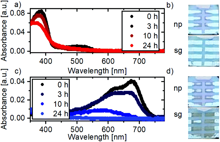 | ||
| Fig. 6 Dry air and sunlight degradation of the HTL. (a) Absorption changes of a PTAA:C60F48 film. (b) Picture of the electrode of a device using PTAA:C60F48 after 42 h of degradation with either ZnO nano-particle or sol–gel as ETL. (c) Absorption changes in PTB7. (d) Pictures of solar cell electrodes employing PTB7 as HTL and either nano-particle or sol–gel ZnO as ETL. | ||
In addition to the changes in the properties of the organic HTL, we observe a significant impact on the Ag electrode. Fig. 6b and d display photographs taken on heavily degraded solar cells with the PTAA:C60F48 and PTB7/MoO3 HTLs, respectively. The pictures show that the rate of degradation of the silver top electrode depends on the choice of HTL. In the case of PTB7/MoO3, the corrosion of the Ag electrode is much more severe as compared to that of PTAA:C60F48 devices. The corrosion of the silver electrode causes the device area to shrink upon degradation time (see Fig. S8†), leading to an additional factor in the reduction of the JSC. Similar corrosion effects of noble electrodes have been observed in perovskite photovoltaics and attributed to halide mediated oxidation processes.33,34
Interestingly, the corrosion also seems to be impacted by the deposition method of the ETL. For example, the electrodes of devices with PTAA:C60F48 and ZnOsg appear largely unaffected, while those with ZnOnp show initial signs of degradation. This suggests that the ETL also plays a role in determining the degradation dynamics of the AgBiS2 NC solar cells.
Role of the ETL on the device stability
ZnO is commonly used as a charge extraction layer in emerging photovoltaic devices based on organic, perovskite and nanocrystal materials.35–41 ZnO on its own is a stable material, for the time frame of this experimental study, and triggers degradation in the active layers mainly due to interfacial effects.37,40 To examine the differences in device stability between the sol–gel and nano-particle based ZnO layers, we first characterised them by atomic force microscopy (AFM). The ZnOnp layer appears rougher, which is to be expected due to its nano-structured nature (Fig. S9†). This might explain the slightly larger JSC observed for ZnOnp-based devices.42 Once the ZnO layers are coated with AgBiS2 NCs, the difference in surface roughness is no longer visible and both ETLs lead to a smooth active layer film. Fig. 7a shows SEM images of AgBiS2 NC films deposited on either ZnOsg or ZnOnp and exposed to oxygen and illumination for different durations of time. While the pristine films appear very similar in both cases, already after 2 h a clear difference can be observed. Relatively few aggregates are being detected on the surface of AgBiS2 when deposited on ZnOsg, but numerous of such aggregates are formed on ZnOnp. After 6 h the film deposited on ZnOnp further degraded, while that on ZnOsg appears similar to the one of 2 h. Finally, after 24 h, some defects and additional aggregates can be observed on the ZnOsg film, while the ZnOnp film is severely degraded. This difference in the rate of AgBiS2 NC active layer degradation depending on the ETL explains the difference in the photovoltaic performance evolution discussed above (Fig. 2). The accelerated degradation of AgBiS2 NC on ZnOnp is further confirmed by the rapid deterioration of their optoelectronic properties and composition of the nanocrystal (see Fig. S10 and S11†). The aggregates themselves are mainly composed of silver and sulphur and are significantly different to the initial composition of the silver bismuth NCs as energy-dispersive X-ray spectroscopy reveals (EDX) (see Fig. S12†). Additionally, the formation of aggregates is connected to the enhanced degradation of an AgBiS2 NC film on a ZnO layer, since, as seen in the optical microscope images, they only form, when a ZnO layer underneath the AgBiS2 is present (Fig. S8†). | ||
| Fig. 7 (a) SEM pictures of a AgBiS2-TMAI NC film on a ITO/ZnOsg (left column) or np (right column) layer during degradation in dry air and sunlight for different time steps. (b) FTIR measurements of a pristine ZnOsg and np film. The OH vibration bands are indicated and the data is offset to each other for better visibility. | ||
Proposed degradation mechanism
The observations made above lead us to propose the following degradation mechanism of AgBiS2 NCs. Globally, the AgBiS2 NCs decompose into bismuth oxide and phase separated silver sulphide upon exposure to oxygen and light: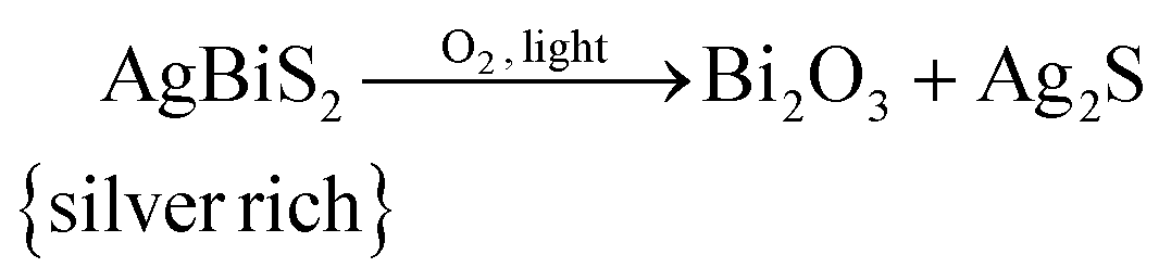
This global degradation path however, would require an oxidation partner for oxygen. Oxidised sulphur species could not be detected (see Fig. 5) in our studies, but we cannot fully exclude this possibility. The iodide containing ligands on the other hand act most likely as redox partner:
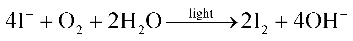
The formation of elemental iodine is likely to be the origin of the observed silver electrode corrosion that irreversibly decomposes the elemental silver.34 This is also confirmed by XPS measurements on Ag electrodes of degraded devices (Fig. S13†):

These proposed redox-reactions will be impacted by the presence of water and surface hydroxyl groups, that could accelerate the global decomposition process of AgBiS2 NCs. Examining the ZnOnp and ZnOsg films by FTIR reveals two absorption bands around 3500 cm−1 and 1500 cm−1, which are significantly stronger for the ZnOnp film. These bands are associated with an increased amount of OH-groups and/or physiosorbed water,43 which accumulate on the surface of the ZnOnp film due to its nano-structured larger surface area. Consequently, the degradation reaction is significantly accelerated.
The impact of humidity on the degradation of AgBiS2 NC solar cells was further explored by performing two control experiments. Fig. S14† shows the evolution of the PCE of devices measured under continuous 1 sun illumination in different environments. In N2 the devices are relatively stable, but in humid N2 they degrade rapidly. Similarly, the addition of 20% relative humidity to dry air results in an accelerated degradation. Since Oh et al. showed well performing AgBiS2 NC solar cells after they were dipped in water for 2 min,19 we believe that the difference arises from the fact that our studies are performed under realistic operational conditions, meaning both bias and 1 sun illumination are continuously applied. We also examined the effect of pre-conditioning prior to the photovoltaic measurements. In this experiment, AgBiS2 NC solar cells with ZnOsg and PTAA:C60F48 were exposed to different environments in the dark for two days prior to testing the operation stability in dry air. Fig. S15† shows the evolution of the JSC which was the only parameter impacted by pre-conditioning. The experiments show that pre-conditioning with either humid air or humid nitrogen leads to an accelerated deterioration in photovoltaic performance despite the fact that the measurement conditions during the operational stability tests were dry. Both these experiments confirm that the presence of water significantly accelerates the decomposition of AgBiS2.
Conclusions
To summarise, we examined the operational stability of AgBiS2 NC solar cells upon exposure to oxygen and light. We identify that the choice of extraction layers dramatically influences the evolution of the photovoltaic performance. In terms of HTL, the commonly used PTB7/MoO3 is significantly less stable than PTAA:C60F48 and is the key contributor to the loss of performance in devices that contain the former. The deposition method of the ZnO ETL also plays a key role, due to the varying amounts of water present at the ZnO surface. Here interlayers of PCBA44,45 or In2O3![[thin space (1/6-em)]](https://www.rsc.org/images/entities/char_2009.gif) 40 could be explored to further improve the device performance and stability. The extraction layers also heavily influence the changes in photophysics during degradation. TA measurements indicate formation of traps with time scales for charge trapping of 100 ps and longer. As the deterioration of performance increases their signature becomes more visible for longer degradation times and both evolutions correlate with the formation of NC decomposition products. We propose that the degradation of the silver rich nanocrystals occurs via the interaction of oxygen with the iodide-containing ligands and results in the degradation of the active layer into bismuth oxide and silver sulphide as well as in corrosion of the silver electrode. The decomposition is accelerated by humidity. The corrosion might be avoidable by the development of new redox-inactive ligands, which should optimally also offer a better passivation in order to yield enhanced performance and stability. These findings highlight the importance of examining the operational stability of devices throughout the development of emerging photovoltaics in order to identify the degradation mechanisms and develop suitable mitigation strategies.
40 could be explored to further improve the device performance and stability. The extraction layers also heavily influence the changes in photophysics during degradation. TA measurements indicate formation of traps with time scales for charge trapping of 100 ps and longer. As the deterioration of performance increases their signature becomes more visible for longer degradation times and both evolutions correlate with the formation of NC decomposition products. We propose that the degradation of the silver rich nanocrystals occurs via the interaction of oxygen with the iodide-containing ligands and results in the degradation of the active layer into bismuth oxide and silver sulphide as well as in corrosion of the silver electrode. The decomposition is accelerated by humidity. The corrosion might be avoidable by the development of new redox-inactive ligands, which should optimally also offer a better passivation in order to yield enhanced performance and stability. These findings highlight the importance of examining the operational stability of devices throughout the development of emerging photovoltaics in order to identify the degradation mechanisms and develop suitable mitigation strategies.
Experimental
Materials
Prepatterned ITO substrates were purchased from PsiOTec. Zinc acetate dihydrate (>98%), 2-methoxyethanol (99%), ethanolamine (99%), silver acetate (99%), bismuth acetate (>99%), and tetramethylammonium iodide (99%) were purchased from Alfa Aesar and used as received. Oleic acid (>90%) and all solvents (99%) were purchased from Thermo Fisher Chemical. PTAA and MoO3 (99.9%) were purchased from Sigma Aldrich. PTB7 was purchased from Ossila. Ag (99.99%) was purchased from Kurt J. Lesker.Nanocrystal synthesis
:1.
Device fabrication
As substrate for solar cells glass with a prepatterned 150 nm thick central ITO layer stripe was used. The substrates were cleaned by sonication in isopropanol and acetone, followed by an oxygen plasma treatment at 100 W, 0.4 mbar for 10 min. The ZnO sol–gel solution was prepared by dissolving 0.46 mol L−1 zinc acetate in 2-methoxyethanol and adding 0.46 mol L−1 ethanolamine. The mixture was stirred at 70 °C for at least 2 h. It was then spin-coated at 2000 rpm for 60 s and annealed at 300 °C for 30 min. The ZnOnp solution with a concentration of 60 mg ml−1 was spin-coated at 3000 rpm for 30 s and annealed at 200 °C for 10 min. The AgBiS2-TMAI NC layer fabrication was performed as described in Bernechea et al.12 and resulted in 30–35 nm thick films. Up until here fabrication of the layer stack took place in air. The organic films were deposited in a nitrogen filled glovebox. PTB7 was spin-coated on top of the NC film from a 5 mg mL−1 solution in anhydrous dichlorobenzene at 2000 rpm for 60 s. PTAA layers were fabricated by 1:1 (vol) mixing a 6 mg mL−1 solution in anhydrous chlorobenzene with a 3 mg mL−1 C60F48 solution in anhydrous chlorobenzene. The doped PTAA was spin-coated at 6000 rpm for 30 s and annealed at 100 °C for 10 min. A 3 nm thick MoO3 layer was evaporated only in the case of the PTB7 HTL, and the final silver electrode was for all devices evaporated at a maximum rate of 0.1 nm s−1 up to 80 nm.
Films for characterisation were fabricated in a similar fashion if not indicated otherwise.
Characterisation
Author contributions
DBK conceptualised the study, fabricated the samples, performed electrical, optical, and optoelectronic characterisation and analysis. MAS measured the SEM pictures, JK measured XPS, and YJH UPS. QA recorded the AFM micrographs. RK performed the TA measurements, supervised by AAB. FP conducted the XRD and FRIT measuerments and assisted in the modelling of the reaction and the writing process. YV supervised the project. DBK and YV wrote the initial draft, all authors contributed to the reviewed draft.Conflicts of interest
There are no conflicts to declare.Acknowledgements
The authors acknowledge financial support by the European Research Council (ERC) under the European Union's Horizon 2020 research and innovation program (ERC Grant Agreements No. 714067, ENERGYMAPS and No. 639750 VIBCONTROL). AAB acknowledges support from Royal Society. We thank the Deutsche Forschungsgemeinschaft (DFG) for funding the project ‘PROCES’ (VA 991/2-1). We would also like to acknowledge the Dresden Center for Nanoanalysis for providing the opportunity to perform electron microscopy, in particular Bernd Rellinghaus and Markus Löffler. Y. V. thanks the Fulbright Commission for support (Fulbright-Cottrell Award 2018).Notes and references
- J. Liu, K. Xian, L. Ye and Z. Zhou, Adv. Mater., 2021, 2008115 CrossRef CAS PubMed.
- O. E. Semonin, J. M. Luther and M. C. Beard, Mater. Today, 2012, 15, 508–515 CrossRef CAS.
- I. Moreels, Y. Justo, B. De Geyter, K. Haustraete, J. C. Martins and Z. Hens, ACS Nano, 2011, 5, 2004–2012 CrossRef CAS PubMed.
- P. R. Brown, D. Kim, R. R. Lunt, N. Zhao, M. G. Bawendi, J. C. Grossman and V. Bulović, ACS Nano, 2014, 8, 5863–5872 CrossRef CAS PubMed.
- G. H. Carey, A. L. Abdelhady, Z. Ning, S. M. Thon, O. M. Bakr and E. H. Sargent, Chem. Rev., 2015, 115, 12732–12763 CrossRef CAS PubMed.
- E. M. Sanehira, A. R. Marshall, J. A. Christians, S. P. Harvey, P. N. Ciesielski, L. M. Wheeler, P. Schulz, L. Y. Lin, M. C. Beard and J. M. Luther, Sci. Adv., 2017, 3, eaao4204 CrossRef PubMed.
- M. Albaladejo-Siguan, D. Becker-Koch, A. D. Taylor, Q. Sun, V. Lami, P. G. Oppenheimer, F. Paulus and Y. Vaynzof, ACS Nano, 2020, 14, 384–393 CrossRef CAS PubMed.
- H. Choi and S. Jeong, Int. J. Precis. Eng. Manuf. Technol., 2018, 5, 349–358 CrossRef.
- I. Celik, Z. Song, A. J. Cimaroli, Y. Yan, M. J. Heben and D. Apul, Sol. Energy Mater. Sol. Cells, 2016, 156, 157–169 CrossRef CAS.
- S. Zheng, J. Chen, E. M. J. Johansson and X. Zhang, iScience, 2020, 23, 101753 CrossRef CAS PubMed.
- H. J. Snaith, Nat. Mater., 2018, 17, 372–376 CrossRef CAS PubMed.
- M. Bernechea, N. C. Miller, G. Xercavins, D. So, A. Stavrinadis and G. Konstantatos, Nat. Photonics, 2016, 10, 521–525 CrossRef CAS.
- L. Hu, R. J. Patterson, Z. Zhang, Y. Hu, D. Li, Z. Chen, L. Yuan, Z. L. Teh, Y. Gao, G. J. Conibeer and S. Huang, J. Mater. Chem. C, 2018, 6, 731–737 RSC.
- I. Burgués-Ceballos, Y. Wang, M. Z. Akgul and G. Konstantatos, Nano Energy, 2020, 75, 104961 CrossRef.
- S. Y. Bae, J. T. Oh, J. Y. Park, S. R. Ha, J. Choi, H. Choi and Y. Kim, Chem. Mater., 2020, 32, 10007–10014 CrossRef CAS.
- M. L. Kelley, F. Ahmed, S. L. Abiodun, M. Usman, M. U. Jewel, K. Hussain, H.-C. zur Loye, M. V. S. Chandrashekhar and A. B. Greytak, ACS Appl. Electron. Mater., 2021, 3, 1550–1555 CrossRef CAS.
- M. Z. Akgul, A. Figueroba, S. Pradhan, Y. Bi and G. Konstantatos, ACS Photonics, 2020, 7, 588–595 CrossRef CAS PubMed.
- M. Albaladejo-Siguan, E. C. Baird, D. Becker-Koch, Y. Li, A. L. Rogach and Y. Vaynzof, Adv. Energy Mater., 2021, 11, 2003457 CrossRef CAS.
- J. T. Oh, S. Y. Bae, S. R. Ha, H. Cho, S. J. Lim, D. W. Boukhvalov, Y. Kim and H. Choi, Nanoscale, 2019, 11, 9633–9640 RSC.
- S. Ming, X. Liu, W. Zhang, Q. Xie, Y. Wu, L. Chen and H.-Q. Wang, J. Cleaner Prod., 2020, 246, 118966 CrossRef CAS.
- D. Becker-Koch, M. Albaladejo-Siguan, Y. J. Hofstetter, O. Solomeshch, D. Pohl, B. Rellinghaus, N. Tessler and Y. Vaynzof, ACS Appl. Mater. Interfaces, 2021, 13(16), 18750–18757 CrossRef CAS PubMed.
- C. H. M. Chuang, P. R. Brown, V. Bulović and M. G. Bawendi, Nat. Mater., 2014, 13, 796–801 CrossRef CAS PubMed.
- D. Becker-Koch, M. Albaladejo-Siguan, V. Lami, F. Paulus, H. Xiang, Z. Chen and Y. Vaynzof, Sustainable Energy Fuels, 2020, 4, 108–115 RSC.
- W. Gao, G. Zhai, C. Zhang, Z. Shao, L. Zheng, Y. Zhang, Y. Yang, X. Li, X. Liu and B. Xu, RSC Adv., 2018, 8, 15149–15157 RSC.
- N. Zhao, T. P. Osedach, L. Chang, S. M. Geyer, D. Wanger, M. T. Binda, A. C. Arango, M. G. Bawendi and V. Bulovic, ACS Nano, 2010, 4, 3743–3752 CrossRef CAS PubMed.
- V. A. Öberg, M. B. Johansson, X. Zhang and E. M. J. Johansson, ACS Appl. Nano Mater., 2020, 3, 4014–4024 CrossRef.
- M. T. Greiner, M. G. Helander, W.-M. Tang, Z.-B. Wang, J. Qiu and Z.-H. Lu, Nat. Mater., 2012, 11, 76–81 CrossRef CAS PubMed.
- S. Liu, X. F. Lu, J. Xiao, X. Wang and X. W. (David) Lou, Angew. Chem., Int. Ed., 2019, 58, 13828–13833 CrossRef CAS PubMed.
- J. Razzell-Hollis, J. Wade, W. C. Tsoi, Y. Soon, J. Durrant and J.-S. Kim, J. Mater. Chem. A, 2014, 2, 20189–20195 RSC.
- Irfan, H. Ding, Y. Gao, C. Small, D. Y. Kim, J. Subbiah and F. So, Appl. Phys. Lett., 2010, 96, 243307 CrossRef.
- M. T. Greiner, L. Chai, M. G. Helander, W.-M. Tang and Z.-H. Lu, Adv. Funct. Mater., 2013, 23, 215–226 CrossRef CAS.
- K. E. Lee, L. Liu and T. L. Kelly, J. Phys. Chem. C, 2014, 118, 27735–27741 CrossRef CAS.
- C. Li, S. Tscheuschner, F. Paulus, P. E. Hopkinson, J. Kießling, A. Köhler, Y. Vaynzof and S. Huettner, Adv. Mater., 2016, 28, 2446–2454 CrossRef CAS PubMed.
- S. Svanström, T. J. Jacobsson, G. Boschloo, E. M. J. Johansson, H. Rensmo and U. B. Cappel, ACS Appl. Mater. Interfaces, 2020, 12, 7212–7221 CrossRef PubMed.
- O. Pachoumi, C. Li, Y. Vaynzof, K. K. Banger and H. Sirringhaus, Adv. Energy Mater., 2013, 3, 1428–1436 CrossRef CAS.
- Y. Sevinchan, P. E. Hopkinson, A. A. Bakulin, J. Herz, M. Motzkus and Y. Vaynzof, Adv. Mater. Interfaces, 2016, 3, 1500616 CrossRef.
- Q. An, P. Fassl, Y. J. Hofstetter, D. Becker-Koch, A. Bausch, P. E. Hopkinson and Y. Vaynzof, Nano Energy, 2017, 39, 400–408 CrossRef CAS.
- A. Weu, T. R. Hopper, V. Lami, J. A. Kreß, A. A. Bakulin and Y. Vaynzof, Chem. Mater., 2018, 30, 2660–2667 CrossRef CAS.
- A. Weu, R. Kumar, J. F. Butscher, V. Lami, F. Paulus, A. A. Bakulin and Y. Yaynzof, Adv. Funct. Mater., 2020, 30, 1907432 CrossRef CAS.
- A. R. Kirmani, F. Eisner, A. E. Mansour, Y. Firdaus, N. Chaturvedi, A. Seitkhan, M. I. Nugraha, E. Yarali, F. P. García de Arquer, E. H. Sargent, T. D. Anthopoulos and A. Amassian, ACS Appl. Energy Mater., 2020, 3, 5135–5141 CrossRef CAS.
- S.-W. Baek, S. Jun, B. Kim, A. H. Proppe, O. Ouellette, O. Voznyy, C. Kim, J. Kim, G. Walters, J. H. Song, S. Jeong, H. R. Byun, M. S. Jeong, S. Hoogland, F. P. García de Arquer, S. O. Kelley, J.-Y. Lee and E. H. Sargent, Nat. Energy, 2019, 4, 969–976 CrossRef CAS.
- S. Pradhan, A. Stavrinadis, S. Gupta, S. Christodoulou and G. Konstantatos, ACS Energy Lett., 2017, 2, 1444–1449 CrossRef CAS.
- G. Nagaraju, Udayabhanu, Shivaraj, S. A. Prashanth, M. Shastri, K. V. Yathish, C. Anupama and D. Rangappa, Mater. Res. Bull., 2017, 94, 54–63 CrossRef CAS.
- Y. Vaynzof, D. Kabra, L. Zhao, P. K. H. Ho, A. T. S. Wee and R. H. Friend, Appl. Phys. Lett., 2010, 97, 033309 CrossRef.
- O. Pachoumi, A. A. Bakulin, A. Sadhanala, H. Sirringhaus, R. H. Friend and Y. Vaynzof, J. Phys. Chem. C, 2014, 118, 18945–18950 CrossRef CAS.
- W. J. E. Beek, M. M. Wienk, M. Kemerink, X. Yang and R. A. J. Janssen, J. Phys. Chem. B, 2005, 109, 9505–9516 CrossRef CAS PubMed.
- D. Becker-Koch, B. Rivkin, F. Paulus, H. Xiang, Y. Dong, Z. Chen, A. A. Bakulin and Y. Vaynzof, J. Phys.: Condens. Matter, 2019, 31, 124001 CrossRef PubMed.
Footnote |
| † Electronic supplementary information (ESI) available. See DOI: 10.1039/d1nr06456h |
| This journal is © The Royal Society of Chemistry 2022 |