
Silicon nitride waveguides with directly grown WS2 for efficient second-harmonic generation†
Ning
Liu‡
 a,
Xi
Yang‡
a,
Zhihong
Zhu
a,
Feng
Chen
b,
Yangbo
Zhou
b,
Jipeng
Xu
a and
Ken
Liu
*a
a,
Xi
Yang‡
a,
Zhihong
Zhu
a,
Feng
Chen
b,
Yangbo
Zhou
b,
Jipeng
Xu
a and
Ken
Liu
*a
aCollege of Advanced Interdisciplinary Studies & Hunan Provincial Key Laboratory of Novel Nano-Optoelectronic Information Materials and Devices, National University of Defense Technology, Changsha 410073, P. R. China. E-mail: liukener@163.com
bSchool of Materials Science and Engineering, Nanchang University, Nanchang 330031, P. R. China
First published on 15th November 2021
Abstract
Different functions can be directly realized by silicon (Si) in integrated electronic circuits. Although Si and silicon nitride (Si3N4) photonics have shown great potential in integrated optoelectronic devices, different functions, such as light generation, transparency for guided light, and light detection, cannot be simultaneously achieved only by Si or Si3N4. Second-order nonlinearity is another optical property they do not possess due to their centrosymmetric properties. Several kinds of 2D materials emerged recently and were transferred to specified photonic devices aimed at improving their nonlinear performance. However, the transferring methods are time-consuming, unable to achieve large-scale production, and will inevitably cause materials damage and introduce impurities at the interface. Herein, we demonstrate the direct growth of large-area homogeneous monolayer WS2via a physical vapor deposition method onto Si3N4 waveguides. The WS2 growth can be controlled mainly along the Si3N4 waveguides and the waveguides show an obvious enhancement of second-harmonic generation with the elongated WS2 coverage. The direct growth of WS2 endows Si3N4 integrated photonics with new nonlinear optical properties. As an alternative method of transferring 2D materials, the method we present here is compatible with large-scale integrated photonic fabrication, which lays the foundation for on-chip integrated optical fabrication and applications.
1. Introduction
Integrated Si and Si3N4 photonics have developed rapidly recently.1–5 However, these materials do not possess an even-order optical nonlinearity due to their centrosymmetric properties, and the lowest nonlinear response is third-order nonlinearity, which limits the applications of Si or Si3N4 photonics in the nonlinear field. Second-harmonic generation (SHG) is a key topic in nonlinear optics and is a process during which twice the frequency of the incident light can radiate from the nonlinear optical medium.6 Some 2D materials, including monolayer transition metal dichalcogenides (TMDCs), possess high second-order nonlinear coefficients due to their broken inversion symmetry. The nonlinear properties of these 2D materials have also been widely studied in theory and application.7–9 One of the great advantages of these 2D materials is that they can be integrated with various materials or structures,10–15 especially with microfibers16–19 and waveguides,20–22 such that SHG enhancement or other enhanced nonlinear processes are realized and analyzed.However, the integrations of 2D materials mentioned above are all realized by transferring methods which are not suitable for large scale production, and the inevitable introduction of impurities during the transferring process will affect the optical performance of these 2D materials. Researchers therefore began to investigate the integration of 2D materials by direct growth, aiming to improve the optical performance of the 2D materials. Large-area monolayer graphene23 and TMDCs24 can be grown directly and uniformly in microstructure fibers, and these kinds of microstructure fibers show excellent nonlinear characteristics. Growing monolayer TMDCs on a Si step was achieved and, based on this method, a FinFET was obtained.25 However, presently to the best of our knowledge, the direct growth of TMDCs on Si3N4 waveguides has not been achieved.
As one kind of TMDC, monolayer WS2 shows excellent optical properties26 and possesses a high second-order nonlinearity.27 For a certain pump power, light intensity can be greatly enhanced at the surface of the Si3N4 waveguide compared with that at a silica microfiber, and SHG should be more efficient in the Si3N4/WS2 waveguide than that in the fiber/WS2 structure (Fig. S1†), since the SHG is proportional to |E|2. Hence, we propose directly growing monolayer WS2 onto on-chip Si3N4 waveguides utilizing physical vapor deposition (PVD) method to realize effective harmonic frequency conversion in the Si3N4/WS2 hybrid waveguide structure.
2. Results and discussion
In this paper, the fundamental transverse electric (TE) mode is analyzed. In the Si3N4 waveguide, the fundamental TE mode has the lowest transmission loss studied in the work. As discussed by Vlasov et al.,28 the TE mode exhibited much lower propagation loss than that for transverse magnetic (TM) mode for a SOI strip waveguide since the TM polarization mode results in an increased interaction with the top surface roughness. Also, a higher order TE mode will increase the interaction with the sidewall surface roughness, resulting in a larger propagating loss.29 Based on the above analysis, we only focus on the fundamental TE mode for the Si3N4 waveguide in this paper. The SHG light component is also assumed to be the fundamental TE mode. When conducting the experiment, we adjusted the polarization of the fiber and the coupling between the fiber and the waveguide to make sure that the fundamental TE mode is propagated in the Si3N4 waveguide.2.1 Growth and characterization of monolayer WS2 on Si3N4 waveguides
In order to grow WS2 directly on the Si3N4 waveguide, as shown in Fig. 1(a), firstly a Si3N4 film with a thickness of 0.6 μm was deposited on the SiO2/Si wafer by means of low-pressure chemical vapor deposition (LPCVD). The required waveguide pattern (waveguides with a width of 2.0 μm and thickness of 0.6 μm) was defined by electron beam lithography (EBL), and then etched by reaction ion etching (RIE). The PVD setup for WS2 growth is shown in Fig. 1(b). WS2 powder (0.4 g) was placed at the upstream of the quartz tube with diameter of 1 inch, and the distance from the WS2 powder to the prepared chip, which was placed in the center of the furnace, was about 7.5 cm. Firstly, 80 sccm of Ar was flowed into the tube for 30 min to ensure a stable and inert chemical reaction environment for the following crystal growth. After that, the 80 sccm of Ar flow was kept unchanged, and the furnace was heated from room temperature to 1160 °C over 50 min, maintained for 15 min for WS2 growth, and cooled to room temperature naturally. The temperature of the furnace is a key factor for the high quality growth of WS2. At 1160 °C, a triangle-shaped monolayer WS2 was grown on the Si3N4 waveguide.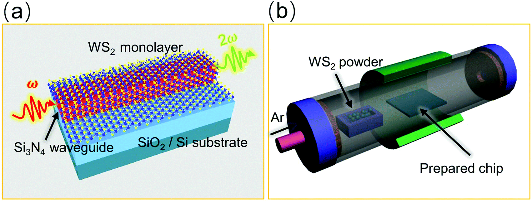 | ||
| Fig. 1 Growth of monolayer WS2 on the Si3N4 waveguide. (a) Schematic of the proposed Si3N4/WS2 hybrid waveguide structure. (b) Schematic of the PVD setup used in the experiment. | ||
The corresponding second harmonic (SH) intensity mapping for the hybrid waveguide in Fig. 2(a) is displayed in Fig. 2(b). When conducting the experiment for SHG mapping (Fig. 2(b)), the input laser was incident normally on the sample and focused on top of the Si3N4 waveguide covered by the grown monolayer WS2. We used Witec Alpha 300R, equipped with a picosecond pulsed laser, and a 20× and a 100× objective lens (N.A. = 0.9) to focus the power on the Si3N4/WS2 hybrid region. Using the confocal technique, we could collect the SHG signal from the focal area and see an obvious SHG signal for the Si3N4/WS2 hybrid region. The PL intensities of WS2 are the same for normal incidence. For the 20× objective lens, the resolution in the vertical direction is low, and thus the WS2 on the waveguide region and the bare WS2 region far away from waveguide have similar PL intensities. While for the 100× objective lens, the resolution in the vertical direction is relatively high, the WS2 on the waveguide region is in the focal plane while the bare WS2 region far away from waveguide is out of the focal plane, and thus the PL intensities from the bare WS2 region are lower than those from the WS2 on the Si3N4 waveguide. The scanning electron microscopy (SEM) image in Fig. 2(c) shows that the WS2 can be grown well on the Si3N4 waveguide. Photoluminescence (PL) and Raman analyses were also performed for the WS2 grown on top of the Si3N4 waveguide using a 532 nm laser, as displayed in Fig. 2(d) and (e). The peak value of the PL spectrum in Fig. 2(d) is located at about 630 nm, and the characteristic peaks of E2g and A1g of monolayer WS2 can be clearly seen from the Raman spectrum shown in Fig. 2(e). Comprehensive analysis from Fig. 2(a)–(e) clearly indicates that monolayer WS2 was directly grown on the Si3N4 waveguide, although there was a 0.6 μm step of the waveguide.
 | ||
| Fig. 2 Characterization of monolayer WS2 grown on the Si3N4 waveguide. (a) Optical microscopy image of a single WS2 crystal grown on the Si3N4 waveguide. (b) The corresponding SH intensity mappings of the structure shown in (a). The Si3N4/WS2 hybrid waveguide region is highlighted by white dashed lines. The image on the right is an enlarged view focused on the waveguide region marked with the dashed white rectangle in the left image. (c) SEM image of monolayer WS2 grown on the Si3N4 waveguide. (d and e) The PL spectrum (d) and Raman spectrum (e) of the monolayer WS2 grown on the Si3N4 waveguide. | ||
2.2 Harmonic generation from monolayer WS2
A femtosecond laser with a central wavelength of about 1570 nm was used to verify the nonlinear property of WS2 and excite the SHG and third harmonic generation (THG) in a monolayer WS2 grown on the SiO2/Si substrate without the Si3N4 waveguide. The schematic of the excitation is shown in the inset in Fig. 3(a). A tapered optical lensed fiber guided the oblique incidence of the excitation light. Although the excitation light was focused to a small area about 4 μm diameter with a very high optical power density, the interaction of the light and the monolayer WS2 was very weak for the oblique incidence. Consequently, the SHG and THG signals were very weak, as shown in Fig. 3(a).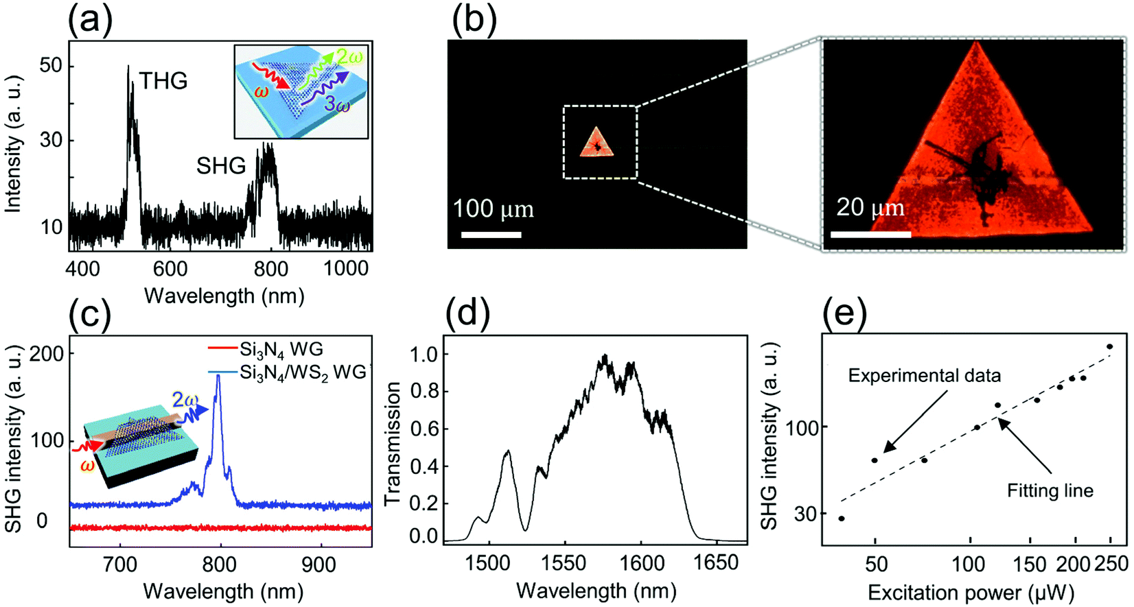 | ||
| Fig. 3 Harmonic generation from monolayer WS2. (a) SHG and THG signals generated from the monolayer WS2 on the SiO2/Si substrate pumped by a femtosecond laser pulse with a center wavelength of 1570 nm. The illustration is a schematic of the oblique incidence on the monolayer WS2. (b) PL images of a single triangular monolayer WS2 crystal grown on the Si3N4 waveguide. The image on the right is an enlarged view focused on the monolayer WS2 region marked with the dashed red rectangle on the left image. Green light emission is excited from the Si3N4 waveguide. (c) Enhanced SHG spectrum of the Si3N4/WS2 hybrid waveguide structure (blue line) and bare Si3N4 waveguide (red line) under a laser pulse excitation centered at 1570 nm. For clarity, the SHG spectrum is upshifted vertically. The illustration is a schematic of the SHG when the edge coupling method is adopted. (d) Corresponding transmission spectrum of the Si3N4/WS2 hybrid waveguide shown in (b). The data are normalized. (e) SHG intensity dependence on the excitation power in the Si3N4/WS2 hybrid waveguide structure. | ||
However, the interaction between the WS2 and light can be greatly enhanced through evanescent field coupling.30,31 Next, we coupled the femtosecond laser to the Si3N4 waveguide with one triangular WS2 crystal grown on the top and both sides adopting an edge coupling method,32 as depicted in the inset in Fig. 3(c). The coupling efficiency of the femtosecond laser to the Si3N4 waveguide was much higher than that of the oblique incidence and thus the harmonic intensity will considerably increase. The photoluminescence (PL) image in Fig. 3(b) verifies the monolayer property of WS2 grown on the Si3N4 waveguide, since multilayer WS2 possesses an indirect bandgap and thus a very low emission efficiency. The Si3N4 does not possess second-order nonlinearity, and the result shows that there was no SHG signal (Fig. 3(c), red line). While for the Si3N4/WS2 hybrid waveguide, the SHG signal with a center wavelength of about 790 nm was apparent (Fig. 3(c), blue line). However, there was no THG signal from the Si3N4/WS2 waveguide, which is because the energy of the third harmonic signal (530 nm or so) exceeds the band gap of monolayer WS2 (about 2 eV),26 and the generated third harmonic signal was absorbed during transmitting in the Si3N4/WS2 hybrid waveguide. However, for Fig. 3(a), a tapered optical lensed fiber guided the oblique incidence of the excitation light to the monolayer WS2, the generated third harmonic signals did not transmit in the waveguide, but emitted directly out of the substrate. As it cannot be absorbed by WS2, the THG signal generated in monolayer WS2 on the SiO2/Si substrate could be collected. Fig. 3(d) is the corresponding transmission spectrum of the femtosecond pulses. Subsequently, we evaluated the harmonic emission intensity dependence of the Si3N4/WS2 waveguide on the excitation power by monitoring the transmission power from 40 to 250 μW, where the quadratic dependence on the excitation power shown in Fig. 3(e) reveals that the collected signal was obviously from the SHG emission.
2.3 Growth of large-area monolayer WS2 on Si3N4 waveguides for further enhanced SHG
As mentioned above, the quality, layers and size of the grown WS2 can be controlled by the temperature. Fig. 4(a)–(c) show the growth results of monolayer WS2 on the Si3N4 waveguides under different temperatures. When we increased the growing temperature from 1160 °C to 1170 °C to 1176 °C, the covered area of monolayer WS2 on the Si3N4 waveguides increased gradually, from a single triangular region (Fig. 3(b)) to several triangular regions (Fig. 4(a)), and then a continuous monolayer WS2 film (Fig. 4(b) and (c)). Fig. 4(b) shows that at 1176 °C, most of the WS2 can be grown along the Si3N4 waveguide. By etching SiO2 at both sides of the Si3N4 waveguide (for the etched structure, see Fig. S2†), a large-area and continuous monolayer of WS2 can be grown on the Si3N4 waveguide, as shown in Fig. 4(c). Also, with the increasing light–matter interaction length, SHG can be enhanced by ∼6–7 times (red line, marked as “waveguide 1” in Fig. 4(a)), and ∼150 times (blue line, marked as “waveguide 2” in Fig. 4(c)), as depicted in Fig. 4(d). It is shown that a higher coverage ratio of WS2 corresponds to more small peaks in the SHG spectrum. This is the result of the interference of light: when WS2 is grown on the Si3N4 waveguides, the refraction index of the waveguide changes. A higher coverage ratio of WS2 corresponds to more small interference peaks. Fig. 4(e) is the corresponding transmission spectrum of the femtosecond pulses. As shown in Fig. 4(e), the transmission spectrum from 1500 nm to 1630 nm also shows interference patterns, which is consistent with the interference patterns from the SHG spectrum. This indicates that the growth of WS2 on the Si3N4 waveguide is inhomogeneous. The interference can be avoided if WS2 is grown homogeneously onto the Si3N4 waveguides.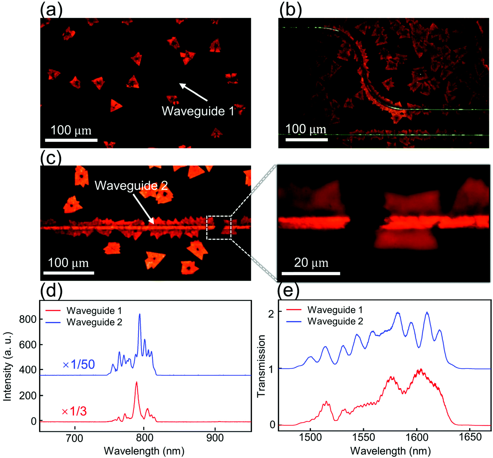 | ||
| Fig. 4 Growth of a large-area of monolayer WS2 on Si3N4 waveguides for an enhanced SHG. (a–c) Dependence of the WS2 covering area on the PVD-growing temperatures of 1170 °C (a), and 1176 °C (b and c). An oblique LED illumination was used in (b) to make the waveguides clearer. The image on the right of (c) is an enlarged view of the Si3N4 waveguide covered by monolayer WS2 marked with the dashed white rectangle in the left image. (d and e) Enhanced SHG (d) and transmission (e) spectra of the Si3N4/WS2 hybrid waveguides under a laser pulse excitation centered at about 1570 nm grown at different temperatures shown in (a) (marked as waveguide 1) and (c) (marked as waveguide 2), respectively. Both spectra are shifted vertically for clarity and the data of (e) are normalized. | ||
Besides, the orientation of the WS2 crystalline will affect the SHG efficiency, as discussed by Chen et al. for monolayer MoSe2 on a silicon waveguide.21 For our research in this paper, the crystalline orientation of monolayer WS2 directly grown onto Si3N4 waveguides is arbitrary and the orientation will undoubtedly affect the SHG intensity. For a certain sample, by adjusting the polarization of the input light, we can obtain the maximum SHG intensity. For the grown large-area WS2, the collected SHG signal is the consequence of the average effect of the crystalline orientation.
3. Conclusions
To conclude, we have proposed a method to directly grow large-area monolayer WS2 onto Si3N4 waveguides. The monolayer properties of the grown WS2 were verified by means of SEM, and PL and Raman spectroscopy. By virtue of the growth of large-area and homogeneous WS2, the enhanced SHG from the Si3N4/WS2 hybrid waveguide was demonstrated. Our work helps to integrate 2D materials with Si3N4 photonics, enrich the optical properties of integrated Si3N4 photonics and pave the way for the large-area growth of 2D materials on integrated circuits.Author contributions
N. L. and X. Y. contributed equally to this work. K. L., N. L. and Z. H. Z. conceived the study. X. Y. and N. L. conducted the experiment of WS2 growth. X. Y. conducted the measurements of Raman spectra. F. C. and Y. B. Z. conducted the experiment of SH mapping. K. L. and N. L. conducted the main measurements. N. L. and J. P. X. drew the schematic diagrams in the paper. N. L. and K. L. led the writing of the paper. All authors discussed the results and commented on the manuscript.Conflicts of interest
There are no conflicts to declare.Notes and references
- J. Leuthold, C. Koos and W. Freude, Nat. Photonics, 2010, 4, 535–544 CrossRef CAS.
- G. T. Reed, G. Mashanovich, F. Y. Gardes and D. J. Thomson, Nat. Photonics, 2010, 4, 518–526 CrossRef CAS.
- A. H. Atabaki, S. Moazeni, F. Pavanello, H. Gevorgyan, J. Notaros, L. Alloatti, M. T. Wade, C. Sun, S. A. Kruger, H. Meng, K. Al Qubaisi, I. Wang, B. Zhang, A. Khilo, C. V. Baiocco, M. A. Popovic, V. M. Stojanovic and R. J. Ram, Nature, 2018, 556, 349–354 CrossRef CAS PubMed.
- X. Li, N. Youngblood, C. Rios, Z. Cheng, C. D. Wright, W. H. P. Pernice and H. Bhaskaran, Optica, 2019, 6, 1–6 CrossRef.
- J. Liu, E. Lucas, A. S. Raja, J. He, J. Riemensberger, R. N. Wang, M. Karpov, H. Guo, R. Bouchand and T. J. Kippenberg, Nat. Photonics, 2020, 14, 486–491 CrossRef CAS.
- G. P. Agrawal, J. Opt. Soc. Am. B, 2011, 28, A1–A10 CrossRef CAS.
- X. F. Liu, Q. B. Guo and J. R. Qiu, Adv. Mater., 2017, 29, 29 Search PubMed.
- X. L. Wen, Z. B. Gong and D. H. Li, InfoMat, 2019, 1, 317–337 CrossRef CAS.
- B. Guo, Q. L. Xiao, S. H. Wang and H. Zhang, Laser Photonics Rev., 2019, 13, 46 Search PubMed.
- A. Majumdar, C. M. Dodson, T. K. Fryett, A. Zhan, S. Buckley and D. Gerace, ACS Photonics, 2015, 2, 1160–1166 CrossRef CAS.
- T. K. Fryett, K. L. Seyler, J. J. Zheng, C. H. Liu, X. D. Xu and A. Majumdar, 2D Mater., 2017, 4, 015031 CrossRef.
- X. T. Gan, C. Y. Zhao, S. Q. Hu, T. Wang, Y. Song, J. Li, Q. H. Zhao, W. Q. Jie and J. L. Zhao, Light: Sci. Appl., 2018, 7, 6 CrossRef.
- J. W. Shi, W. Y. Liang, S. S. Raja, Y. G. Sang, X. Q. Zhang, C. A. Chen, Y. R. Wang, X. Y. Yang, Y. H. Lee, H. Ahn and S. Gwo, Laser Photonics Rev., 2018, 12, 7 Search PubMed.
- J. W. Chen, K. Wang, H. Long, X. B. Han, H. B. Hu, W. W. Liu, B. Wang and P. X. Lu, Nano Lett., 2018, 18, 1344–1350 CrossRef CAS PubMed.
- Q. C. Yuan, L. Fang, H. L. Fang, J. T. Li, T. Wang, W. Q. Jie, J. L. Zhao and X. T. Gan, ACS Photonics, 2019, 6, 2252–2259 CrossRef CAS.
- P. G. Yan, A. J. Liu, Y. S. Chen, H. Chen, S. C. Ruan, C. Y. Guo, S. F. Chen, I. L. Li, H. P. Yang, J. G. Hu and G. Z. Cao, Opt. Mater. Express, 2015, 5, 479–489 CrossRef.
- Y. Z. Wang, F. Zhang, X. Tang, X. Chen, Y. X. Chen, W. C. Huang, Z. M. Liang, L. M. Wu, Y. Q. Ge, Y. F. Song, J. Liu, D. Zhang, J. Q. Li and H. Zhang, Laser Photonics Rev., 2018, 12, 9 Search PubMed.
- J. H. Chen, J. Tan, G. X. Wu, X. J. Zhang, F. Xu and Y. Q. Lu, Light: Sci. Appl., 2019, 8, 8 CrossRef.
- B. Q. Jiang, Z. Hao, Y. F. Ji, Y. G. Hou, R. X. Yi, D. Mao, X. T. Gan and J. L. Zhao, Light: Sci. Appl., 2020, 9, 8 CrossRef.
- L. H. Liu, K. Xu, X. Wan, J. B. Xu, C. Y. Wong and H. K. Tsang, Photonics Res., 2015, 3, 206–209 CrossRef CAS.
- H. T. Chen, V. Corboliou, A. S. Solntsev, D. Y. Choi, M. A. Vincenti, D. de Ceglia, C. de Angelis, Y. R. Lu and D. N. Neshev, Light: Sci. Appl., 2017, 6, 7 Search PubMed.
- Y. J. Zhang, L. Tao, D. Yi, J. B. Xu and H. K. Tsang, J. Opt., 2020, 22, 5 Search PubMed.
- K. Chen, X. Zhou, X. Cheng, R. X. Qiao, Y. Cheng, C. Liu, Y. D. Xie, W. T. Yu, F. R. Yao, Z. P. Sun, F. Wang, K. H. Liu and Z. F. Liu, Nat. Photonics, 2019, 13, 754–759 CrossRef CAS.
- Y. G. Zuo, W. T. Yu, C. Liu, X. Cheng, R. X. Qiao, J. Liang, X. Zhou, J. H. Wang, M. H. Wu, Y. Zhao, P. Gao, S. W. Wu, Z. P. Sun, K. H. Liu, X. D. Bai and Z. F. Liu, Nat. Nanotechnol., 2020, 15, 987–988 CrossRef CAS.
- M. L. Chen, X. D. Sun, H. Liu, H. W. Wang, Q. B. Zhu, S. S. Wang, H. F. Du, B. J. Dong, J. Zhang, Y. Sun, S. Qiu, T. Alava, S. Liu, D. M. Sun and Z. Han, Nat. Commun., 2020, 11, 7 CrossRef.
- H. L. Liu, C. C. Shen, S. H. Su, C. L. Hsu, M. Y. Li and L. J. Li, Appl. Phys. Lett., 2014, 105, 4 Search PubMed.
- C. Janisch, Y. X. Wang, D. Ma, N. Mehta, A. L. Elias, N. Perea-Lopez, M. Terrones, V. Crespi and Z. W. Liu, Sci. Rep., 2014, 4, 5 Search PubMed.
- Y. A. Vlasov and S. J. McNab, Opt. Express, 2004, 12, 1622–1631 CrossRef PubMed.
- X. Ji, J. K. Jang, U. D. Dave, M. Corato-Zanarella, C. Joshi, A. L. Gaeta and M. Lipson, Laser Photonics Rev., 2021, 15, 2000353 CrossRef CAS.
- J. L. Kou, J. H. Chen, Y. Chen, F. Xu and Y. Q. Lu, Optica, 2014, 1, 307–310 CrossRef.
- S. J. Koester and M. Li, IEEE J. Sel. Top. Quantum Electron., 2014, 20, 84–94 Search PubMed.
- V. R. Almeida, R. R. Panepucci and M. Lipson, Opt. Lett., 2003, 28, 1302–1304 CrossRef CAS.
Footnotes |
| † Electronic supplementary information (ESI) available. See DOI: 10.1039/d1nr06216f |
| ‡ These authors contributed equally to this work. |
| This journal is © The Royal Society of Chemistry 2022 |