
Stacking-dependent optical properties in bilayer WSe2†
Kathleen M.
McCreary
 *a,
Madeleine
Phillips
a,
Hsun-Jen
Chuang
b,
Darshana
Wickramaratne
a,
Matthew
Rosenberger
c,
C. Stephen
Hellberg
a and
Berend T.
Jonker
a
*a,
Madeleine
Phillips
a,
Hsun-Jen
Chuang
b,
Darshana
Wickramaratne
a,
Matthew
Rosenberger
c,
C. Stephen
Hellberg
a and
Berend T.
Jonker
a
aNaval Research Laboratory, Washington, DC 20375, USA. E-mail: kathleen.mccreary@nrl.navy.mil
bNova Research, Inc., Washington, DC 20375, USA
cUniversity of Notre Dame, Notre Dame, IN 46556, USA
First published on 6th December 2021
Abstract
The twist angle between the monolayers in van der Waals heterostructures provides a new degree of freedom in tuning material properties. We compare the optical properties of WSe2 homobilayers with 2H and 3R stacking using photoluminescence, Raman spectroscopy, and reflectance contrast measurements under ambient and cryogenic temperatures. Clear stacking-dependent differences are evident for all temperatures, with both photoluminescence and reflectance contrast spectra exhibiting a blue shift in spectral features in 2H compared to 3R bilayers. Density functional theory (DFT) calculations elucidate the source of the variations and the fundamental differences between 2H and 3R stackings. DFT finds larger energies for both A and B excitonic features in 2H than in 3R, consistent with experimental results. In both stacking geometries, the intensity of the dominant A1g Raman mode exhibits significant changes as a function of laser excitation wavelength. These variations in intensity are intimately linked to the stacking- and temperature-dependent optical absorption through resonant enhancement effects. The strongest enhancement is achieved when the laser excitation coincides with the C excitonic feature, leading to the largest Raman intensity under 514 nm excitation in 2H stacking and at 520 nm in 3R stacked WSe2 bilayers.
Introduction
Two-dimensional transition metal dichalcogenides (TMDs) are an exciting class of materials that exhibit unique optical,1,2 electronic,3,4 and valleytronic5–7 properties and have captivated researchers for the last decade. These layered materials are defined by the chemical formula MX2, where M is a metal and X is a chalcogen. A TMD monolayer is actually three atomic layers thick, exhibiting a trigonal prismatic geometry where the outer chalcogen layers are covalently bonded to the central metal atom. Out of plane bonding between monolayers is governed by the relatively weak van der Waals forces. However, these interlayer interactions are strong enough that altering the stacking geometry can significantly modify the measured properties of TMD bilayers.Several semiconducting TMD materials, including WSe2, exhibit a transition from direct band gap to indirect band gap upon increasing from one to two layers. Monolayers have received the bulk of attention thus far for applications ranging from chemical sensing5 to quantum emission.6 However, WSe2 bilayer TMDs are particularly attractive for use in piezoelectric applications,7 valleytronics,8 photodetectors,9 and transistors,10 in part due to their improved stability and higher carrier mobility. Additionally, bilayer systems exhibit an added degree of freedom: the twist angle. While early experimental works largely investigated the naturally occurring 2H stacking order11,12 because of the reliance on mechanically exfoliated WSe2, recent advances in synthesis13–15 and sequential stacking processes16 are opening the door to investigations of 3R stacked bilayers and twisted bilayer systems. The atomic positions in 2H and 3R WSe2 are shown schematically in Fig. 1a and b. Recent optical studies noted differences between 2H and 3R stacked bilayers in the photoluminescence emission associated with direct K–K transitions,17 suggesting the orientation between layers may provide a way to controllably tune properties. However, the impact of stacking order on other optical properties was not addressed, and contradictory behaviors were later observed in other PL studies,16 where PL emission energies of the K–K transition were the same for 2H and 3R stacking orders. Both studies employed sequential stacking to fabricate bilayers, which is susceptible to interlayer contaminants18 as well as angle misalignments which could complicate the interpretation of data.
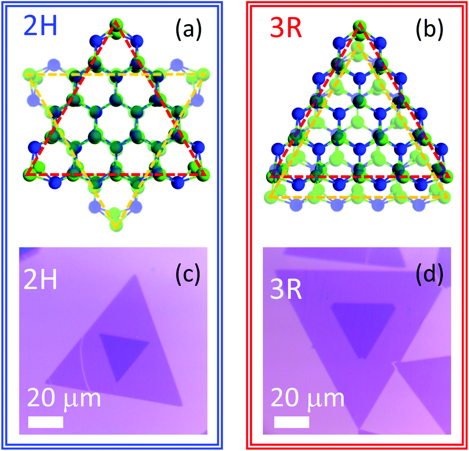 | ||
| Fig. 1 (a and b) Schematic drawings showing atomic positions for WSe2 bilayers with 2H and 3R stacking order, respectively. Selenium atoms are depicted in green and tungsten in blue. Representative optical images of (c) 2H and (d) 3R WSe2 bilayer samples. | ||
Here we provide a comprehensive investigation of the Raman, photoluminescence, and reflectance contrast response of 2H and 3R WSe2 bilayers grown by chemical vapor deposition (CVD). The use of CVD ensures clean residue-free interlayer interfaces and precise stacking orientation which are difficult to insure in bilayers assembled by transfer processes. Clear stacking-dependent differences are evident in all optical properties in CVD-grown bilayers, and properties discussed in this work can serve as a point of reference for homobilayers assembled by mechanical transfer.
Results and discussion
WSe2 bilayers are obtained via chemical vapor deposition at a growth temperature of 825 °C on SiO2/Si substrates, similar to previously reported processes.19 Solid WO3 (1000 mg, Alfa Aesar 99.999%) and solid selenium (500 mg, Alfa Aesar 99.999%) serve as precursors for the growth. Additional details are provided in the Methods. The high growth temperatures along with differences in the thermal expansion coefficients between SiO2 and transition metal dichalcogenides produces tensile strain in WSe2 following synthesis.20,21 To remove the strain, all bilayer samples are picked up from the growth substrate using a polymer stamp transfer process and subsequently placed on fresh SiO2/Si.22As is evident in Fig. 1c and d, WSe2 islands containing both monolayer and bilayer regions are produced. Notably, the inner bilayer region and larger outer monolayer equilateral triangles exhibit one of two orientations, either at a 60 degree angle or rotationally aligned to one another. These two sample types correspond to the different stacking orders, 2H and 3R, respectively.23 Imperfections such as wrinkles, cracks, or tears, can be introduced during the transfer process. However, regions that are free of macroscopic defects or deformations are readily available in both 2H and 3R bilayer stacks and typically exhibit lateral dimensions on the order of several microns to tens of microns, enabling reliable optical measurements.
The optical properties of representative 2H and 3R WSe2 bilayers are investigated using a commercial Horiba LabRam Evolution confocal spectrometer integrated with a closed cycle Montana optical cryostat. A 50× objective focuses the desired illumination source to a spot having approximately 2 μm diameter on the sample. Raman spectroscopy, photoluminescence (PL) measurements, and reflectance data are all collected at the same spot on each sample. 532 nm excitation is used for Raman and PL measurements, with laser power at the sample kept below 100 μW for all measurements. For reflectance measurements, a broad band white light source is focused through the objective onto the sample and the reflected intensity is measured. To minimize unwanted contributions from the substrate, we determine the reflectance contrast RC = (Roff − Ron)/Roff, where Ron is the reflectance of the WSe2 sample on the SiO2 substrate and Roff is the reflectance of the bare SiO2 substrate.
The room temperature Raman spectra of both 2H and 3R bilayer stacking orders exhibit a dominant A1g mode at 251 cm−1, as well as a second, much weaker, feature at 259 cm−1 associated with the 2LA(M) mode, consistent with previous reports for bilayer WSe2.24,25 However, in our direct comparisons between the stacking orders, clear differences are evident. The A1g intensity of 2H WSe2 bilayer (blue line, Fig. 2a) is a factor of three larger than in the 3R bilayers (red line, Fig. 2a) under identical excitation conditions. The smaller A1g intensity present in 3R WSe2 allows for the detection of the nearly degenerate E2g mode, as shown in the multi-component fittings of the normalized spectra (Fig. 2b and c). Bilayers with 2H stacking are well fit by a single Lorentzian at 251.0 cm−1 and a Gaussian at 259.8 cm−1, attributed to the A1g and second order 2LA(M) modes, respectively. However, bilayers of 3R stacking exhibit a low wavenumber shoulder, requiring two Lorentzian curves at 249.6 cm−1 and 251.3 cm−1 to adequately fit the spectra, as shown in Fig. 2c, attributed to the E2g and A1g modes. These differences between the stacking orders are consistently observed across multiple samples (ESI Fig. S1†). The stacking order also impacts the low frequency shear and layer-breathing modes (ESI Fig. S2†), consistent with previous investigations.26,27
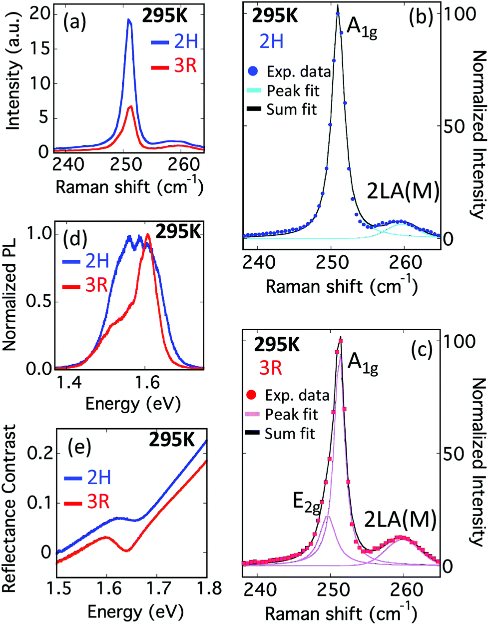 | ||
| Fig. 2 Room temperature Raman, PL and reflectance contrast spectra of bilayer WSe2. 532 nm excitation is used for Raman and PL measurements. (a) The Raman intensity of 2H stacking is a factor of 3 larger than for 3R stacking. (b) Bilayers with 2H stacking are well fit by a single Lorentzian at 251.0 cm−1 and Gaussian at 259.8 cm−1, attributed to the A1g modes and second order 2LA(M) modes, respectively. (c) Bilayers of 3R stacking exhibit a low wavenumber shoulder, requiring two Lorentzian curves at 249.6 cm−1 and 251.3 cm−1 along with a Gaussian at 259.8 cm−1 to adequately fit the spectra, attributed to the E2g, A1g and 2LA(M) modes, respectively. (d) Photoluminescence spectra exhibit clear differences in line shape. (e) In reflectance contrast spectra, the A-exciton is evident at 1.66 eV in 2H and 1.64 eV in 3R bilayers. All data are acquired after samples have been transferred to a fresh SiO2/Si substrate to remove strain. | ||
Both PL and reflectance contrast measurements reveal clear differences between the optical behavior of the 2H and 3R stacking orders. The PL spectra (Fig. 2d) suggest the presence of multiple emission features in both stacking orders, with higher energy features likely associated with direct-gap transitions and lower energy features indirect-gap transitions. In 3R WSe2, the emission features at higher energy exhibit significantly stronger emission relative to the lower energy features. In contrast, all emission components exhibit similar strength for 2H samples, leading to fundamentally different PL line shapes between the 2H and 3R samples. In addition, the emission extends to higher energy for the 2H samples. The absolute intensity of PL emission exhibits some sample-to-sample variation, but the distinctly different line shapes are consistently observed between 2H and 3R (ESI Fig. S3†). Reflectance contrast measurements (Fig. 2e) find a dip centered at 1.66 eV (1.64 eV) for 2H (3R) WSe2 bilayers, consistent with PL extending to higher energies for 2H stacking. These features are associated with the direct-gap A exciton at the K point in the Brillouin zone. The small absorption coefficient of the indirect gap transition prevents its detection in reflectance contrast measurements and any features at higher energy are indistinguishable from the background level.
To further elucidate these observations, measurements are repeated at 4 K. As is evident in Fig. 3a, the low temperature reflectance contrast spectra reveal three clear features at 1.72 eV (1.71 eV), 2.18 eV (2.15 eV), and 2.42 eV (2.37 eV) for 2H(3R) stacking orders. Following previous convention, we label these as A, B, and C features, respectively.28 The A and B excitons arise from spin- and layer-matched transitions at the K point. Specific transitions corresponding to the A and B excitons in each bilayer are illustrated in Fig. S7.† The C feature has previously been experimentally reported in WSe2,28,29 but the precise origin remains unclear. However, it is thought that the C feature originates from a band nesting region where valence and conduction bands are nearly parallel, leading to numerous optical transitions that are nearly degenerate in energy.29–32 Here, we find the A, B, and C features are systematically at higher energy in 2H materials than in 3R, with the difference monotonically increasing from 10 meV for A to 50 meV for C.
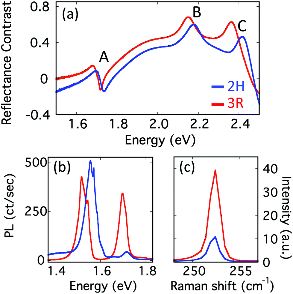 | ||
| Fig. 3 (a) Reflectance contrast, (b) PL, and (c) Raman of bilayer WSe2 at 4 K. 532 nm excitation is used for Raman and PL measurements. 2H orientation is displayed in blue and 3R in red. | ||
The corresponding photoluminescence at 4 K (Fig. 3b) finds features in 2H WSe2 that are blue-shifted relative to similar features in the 3R sample. In both stacking orders, two well-separated features are evident. The peak at 1.71 eV (1.70 eV) for 2H (3R) matches well with the A exciton energy observed in reflectance contrast, indicating this feature is associated with the direct-gap A exciton. The second feature for 2H (3R) is centered around 1.56 eV (1.52 eV) and associated with indirect transitions. Notably, for both PL and reflectance contrast, the general behaviors remain the same across the investigated temperature range, with features in 2H WSe2 always blue-shifted relative to their 3R counterpart.
In contrast, temperature considerably changes the behavior observed in the Raman spectra (Fig. 3c). At 4 K, the dominant A1g Raman mode at 252 cm−1 is four times stronger in 3R WSe2 than in 2H, a reversal from the room temperature behavior where this mode was three times stronger in the 2H (Fig. 2a). To elucidate this behavior, additional measurements are acquired under a variety of excitation wavelengths between 488 nm and 588 nm (Fig. 4). All data are normalized to the Si Raman peak at 523 cm−1 to allow for direct comparison of the A1g intensity11 and all laser powers are kept below 100 μW, to prevent sample damage. It is immediately evident that the resulting A1g intensity depends strongly on the excitation wave length used. In both 2H and 3R systems, large intensities are achieved for laser excitation wavelength between 514 nm and 532 nm (highlighted by the dashed blue box in Fig. 4). Laser excitations well above or well below this range lead to significantly lower A1g intensity. Additionally, the conditions leading to maximum A1g intensity are different for the two stacking orders, with 2H exhibiting highest signal for 514 nm excitation while the maximum in 3R WSe2 is achieved for 520 nm excitation based on the discrete wavelengths used here. The intensity of the Raman B12g mode shows a similar excitation-dependent behavior, as detailed in ESI Fig. S4 and S5.†
 | ||
| Fig. 4 Low-temperature (4 K) excitation-dependent Raman of WSe2 bilayers for (a–h) 2H and (i–p) 3R stacking orientation. All spectra are normalized to Si Raman intensity at 523 cm−1 and excitation wavelength is indicated in the upper right corner. Under 532 nm excitation, the A1g mode exhibits higher intensity in 3R than 2H samples, contrary to the room temperature behavior presented in Fig. 2a. Excitation from 514 nm to 532 nm leads to notably large A1g intensities in both 2H and 3R orientations, highlighted by the blue dashed box. However, in 2H samples the maximum intensity is evident for 514 nm excitation and for 3R maximum is evident under 520 nm excitation. | ||
The detailed A1g intensity as a function of excitation wavelength is presented in Fig. 5a. Upon comparison with the reflectance contrast data replotted as a function of wavelength (Fig. 5b), it is apparent that the Raman intensity and the reflectance contrast follow the same trend. The strongest enhancement occurs when the excitation wavelength coincides with the C exciton in the reflectance contrast spectra. A second enhancement, although to a much lesser degree, is also present near the B exciton feature. Similar resonantly enhanced Raman has been reported in mechanically exfoliated materials having 2H stacking,11,33 but has not been investigated in 3R stacking orders. The C exciton resonant enhancement of Raman also clarifies the reason the 2H shows stronger A1g mode at room temperature and 3R shows stronger A1g mode at low temperature. As evident in Fig. 5a, 532 nm excitation (dashed line) is considerably closer to resonance with the C exciton feature in 3R stacking than in 2H stacking, leading to larger Raman enhancement in 3R WSe2 at low temperature. However, as temperature increases, red shifts are expected in all excitonic features. The 4 K (Fig. 3a) and room temperature (Fig. 2e) reflectance contrast spectra show the A exciton red-shifting by about 30 nm. A similar shift would lead to room temperature C exciton peak positions at approximately 542 nm in 2H and 553 nm in 3R, consistent with our observations of larger Raman intensity in 2H than 3R WSe2 at room temperature with 532 nm excitation (Fig. 2a). Thus the intrinsic differences in Raman intensity between the 2H and 3R stacking (e.g. at 488 nm, Fig. 4a and i) are strongly modulated by resonance effects when the excitation energy is near resonance with the temperature dependent absorption edges.
 | ||
| Fig. 5 Low-temperature (a) excitation-dependent Raman intensity of the A1g mode and (b) reflectance contrast, RC, plotted as a function of wavelength. The Raman enhancements in 2H and 3R WSe2 orientations coincide well with the C exciton feature in the reflectivity spectra. | ||
To provide insight into the intimate relationship between the changes in stacking and the reflectance contrast, PL, and Raman of bilayer WSe2, we perform density functional theory (DFT) calculations (see the Methods section for calculation details). We computed band structures for both the 2H and 3R bilayer (Fig. 6a and b). We note that 3R bilayers lack inversion symmetry and may be present in two distinct geometries: AB and BA (Fig. S6†). The impact of the lack of inversion symmetry can be clearly seen in the conduction and valence band splitting in the 3R band structure, which is not present in the 2H bands (Fig. 6). This splitting is due to the different atomic environments of the tungsten atoms in each layer of a 3R-stacked bilayer; it has the same magnitude in the AB and BA structures, with only the layer polarization switched (Fig. S6†). While the predicted splitting is not evident in samples on SiO2/Si substrates (Fig. 2 and 3), this is likely due to inhomogeneous broadening arising from detrimental substrate effects.34 To address the effect of the substrate, a single WSe2 flake containing both 2H and 3R stacking orientations is selected and encapsulated with hexagonal boron nitride. Additionally, an AFM tip is used to nano-squeegee a rectangular 20 by 25 μm region (Fig. 7a). This procedure effectively removes contaminants and improves the homogeneity across the sample,35 as evident by the AFM topography shown in Fig. 7b. The low temperature (4 K) reflectance contrast is measured at the 14 locations and presented in Fig. 7c. Notably, a clear splitting of approximately 17 meV is repeatably observed in 3R bilayers only. The two peaks correspond to distinct A excitons in the upper and lower layers and are consistent with the 12 meV splitting observed in DFT calculations. The higher temperature experiments as well as investigations of samples that have not been encapsulated in hBN only show a single A exciton peak for the 3R structures, which can be understood as an average of the layer-polarized exciton peaks. We therefore present results only for the 3R AB structure in Fig. 6. When relating our calculations to our experimental results, we compare energy differences between experimentally measured excitons in 2H- and 3R-stacked bilayers with differences in the calculated single-particle band gaps of the 2H- and 3R-stacked systems. While calculations at the GW-BSE level of theory are required to obtain quantitative values for the exciton energies36 differences in single-particle band gaps are a meaningful quantity if the exciton binding energies of the materials under comparison are nearly identical. From our first-principles calculations we find the interlayer separation (defined as the shortest vertical distance between the Se atoms at the van-der-Waals interface) to be 3.152 Angstroms for the 2H structure and 3.165 Angstroms for the 3R structure. Since we find the interlayer separation in the 2H and 3R structures to be approximately the same (differing by 0.01 Angstroms) this suggests the dielectric properties and in turn the exciton binding energies for the 2H and 3R structures will be similar. This allows us to compare changes in the single-particle band gaps of our first-principles calculations with our experiments.
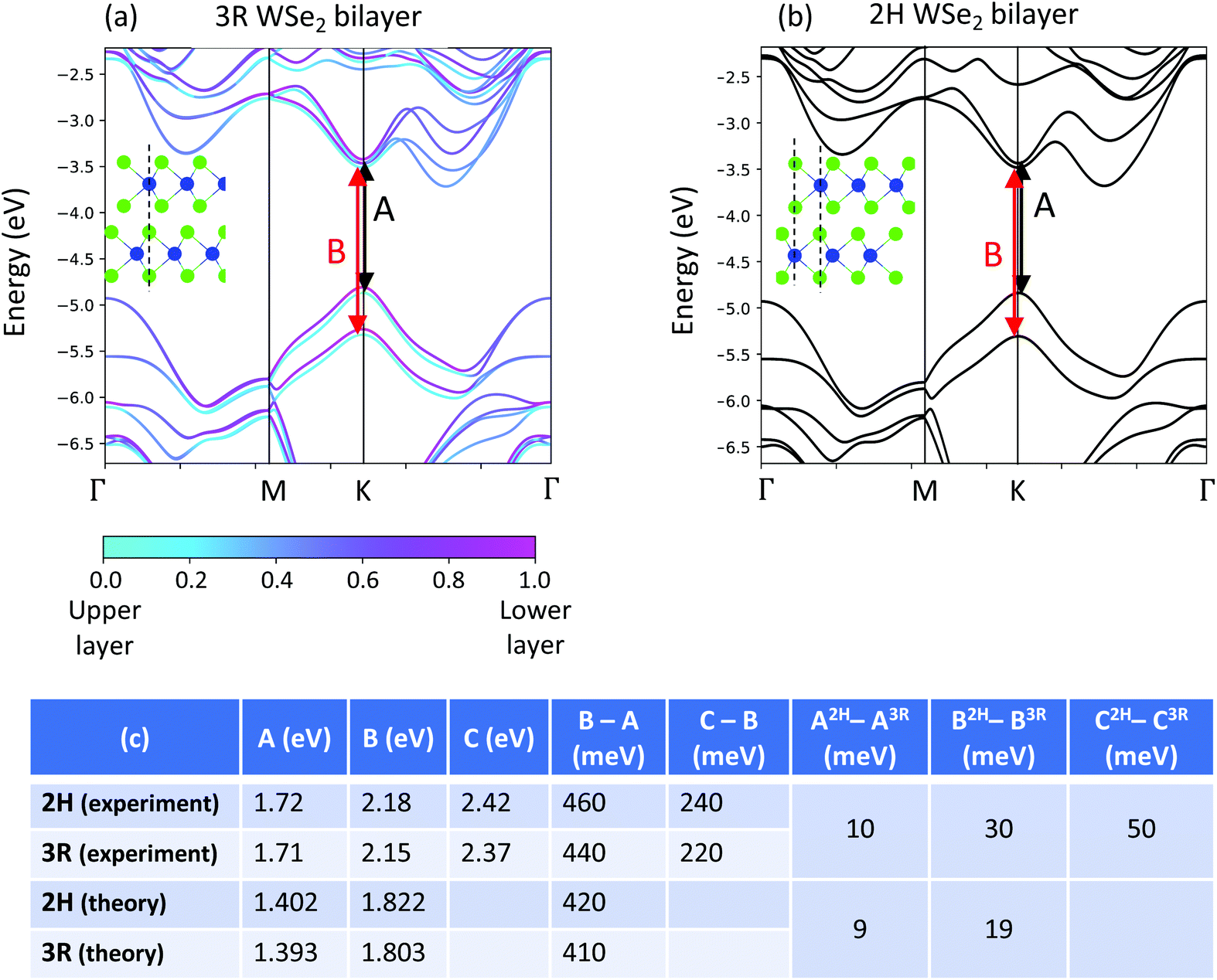 | ||
| Fig. 6 DFT calculations for (a) the 3R bilayer and (b) the 2H bilayer. Insets show the side view of a schematic of each stacking. Black (red) arrows show the origin in the band structure of the A and B excitons. All bands in the 2H bilayer are doubly degenerate, where each state in a degenerate pair may be layer-polarized or layer delocalized. All bands are aligned to the vacuum level. (c) The table compares theoretical and experimental values for the band gaps. Although PBE-level theory underestimates band gaps, the differences in gap size agree well with differences in exciton energies measured in experiment. | ||
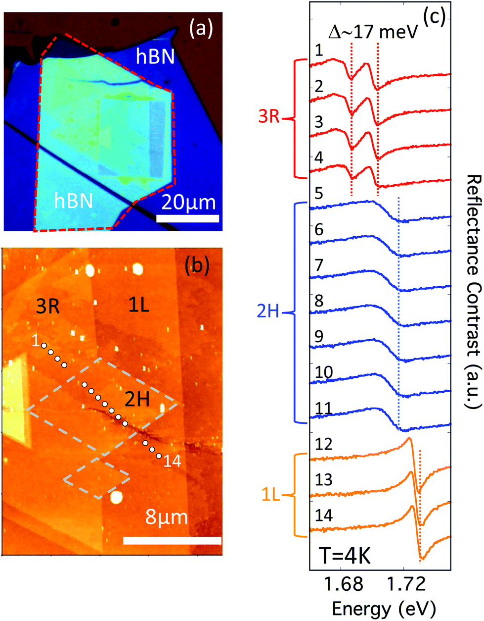 | ||
| Fig. 7 Investigation of hBN-encapsulated WSe2. (a) Optical image of the fabricated device. A WSe2 flake containing both 2H and 3R bilayer WSe2 is selected. The WSe2 has been transferred onto thick hBN >20 nm (dark blue contrast) and covered with hBN ∼14.5 nm (indicated by the dashed red line). An AFM tip is used to nano-squeegee the sample across a 20 by 25 μm region. (b) The AFM topography of the nano-squeegeed region. 3R and 2H regions show no difference in topography, but are identified by rotation angle. Two regions of 2H stacking are outlined in grey dashes for clarity. The reflectance contrast spectra are acquired at T = 4 K from the 14 locations indicated by circles. (c) The 4 K reflectance contrast spectra from 3R bilayer are displayed in red, 2H bilayer in blue and monolayer in orange. Notably, 3R WSe2 shows two clear absorption features separated by ∼17 meV, consistent with the energy difference of upper and lower layer A excitons computed in DFT (Fig. S6†). | ||
We approximate the A exciton values in our bilayers by computing the “A” band gaps in each layer of the bilayer of a given structure and taking the average. We follow the same procedure for the B excitons. We compute “A” band gap values of 1.402 eV for 2H and 1.393 eV for 3R. The 2H “A” band gap is 9 meV higher than the 3R “A” band gap, which agrees with the 2H A exciton being ∼10 meV higher than the 3R A exciton as shown in both our reflectance contrast and PL measurements at 4 K. We compute “B” band gap values of 1.822 eV for the 2H structure and 1.803 eV for the 3R structure, so the 2H “B” band gap is 19 meV larger than the 3R “B” band gap. This is in agreement with the 2H B exciton being 30 meV higher than the 3R B exciton in low-temperature reflectance contrast. The energy difference between the A and B exciton features measured in the 4 K reflectance contrast experiment is 460 meV in the 2H structure and 440 meV in the 3R structure. This is also in good agreement with our calculated values of (B–A)2H = 420 meV and (B–A)3R = 410 meV. Although first-principles calculations that use the GGA functional are known to underestimate the band gaps of the semiconducting TMDs,37 we find that differences in our computed band gaps are consistent with our experiments (Fig. 6c).
The increased value of (B–A)2H compared to (B–A)3R can be understood by considering the difference in interlayer hopping in the two stacking configurations. The largest-magnitude difference in the band structures of the two stackings is in the valence band splitting. This difference can be understood as a consequence of the symmetry of the tungsten d-orbitals that dominate at the valence band edges at K. Due to the different alignment of the K and K′ points in 2H vs. 3R, interlayer hopping is allowed in the 2H structure and forbidden in the 3R structure at the K/K′ points.8,38 The interlayer hopping in 2H increases the valence band splitting relative to the 3R valence band splitting at K. Following the method outlined in ref. 39 we use the valence band splittings of 468 meV for 2H and 454.5 meV for 3R stackings from our DFT calculations to estimate an interlayer hopping in the 2H structure of t⊥ = 56 meV, which is in good agreement with other theoretical estimations of this value in the literature40 when accounting for different choices in lattice constant in the calculations. If we assume the experimental B–A value is a reasonable proxy for valence band splitting in each stacking, we would estimate an interlayer hopping in the 2H structure as 67 meV, which is also of the same order of magnitude as calculated values.
We now turn to understanding the spectral dependence of the Raman intensity and the differences due to 2H and 3R stacking. We calculate the zone center vibrational modes of 2H and 3R bilayer WSe2 and the Raman cross section for the A1g and Eg modes of the bilayer structure (see Methods).
For the 2H structure we find the A1g mode at 246 cm−1 and the E2g mode at 242 cm−1. For the 3R AB and BA structures we calculate the A1g mode to be 245 cm−1 and the E2g mode at 242 cm−1. The calculated vibrational frequencies of A1g and E2g modes for both stackings are near-degenerate and are close to the experimentally measured frequency of 251 cm−1. We calculate the cross section, S(ω), which is directly proportional to the Raman intensity, for the A1g and E2g modes of the 2H and 3R (AB and BA) structures. The magnitudes of S(ω) for the 3R AB and BA structures are similar, hence we only present results for the 3R AB structure. We find S(ω) for the E2g mode is more than an order of magnitude lower compared to S(ω) for the A1g mode for the 2H and 3R structures. Hence, we only focus on S(ω), of the A1g mode of the 2H and 3R (AB) structure, which is illustrated in Fig. 8(b). Two caveats are in place. First, to account for the underestimation of the band gap in our GGA calculations, the cross-sections are blue-shifted so that the onset in the GGA dielectric functions used to calculate S(ω) coincide with GW calculations of the A exciton of monolayer WSe2![[thin space (1/6-em)]](https://www.rsc.org/images/entities/char_2009.gif) 41 (commonly referred to as a scissors shift). Secondly, since we do not include the role of excitons this precludes an investigation of the potential role of the excited states of excitons in resonant Raman processes.
41 (commonly referred to as a scissors shift). Secondly, since we do not include the role of excitons this precludes an investigation of the potential role of the excited states of excitons in resonant Raman processes.
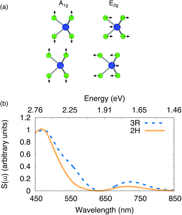 | ||
| Fig. 8 (a) Schematic illustration of the side view of the 2H WSe2 bilayer illustrating the A1g and E2g modes with black arrows. (b) Raman cross section of the A1g mode of WSe2 in the 2H (orange – solid line) and 3R (blue – dotted line) stacking configuration normalized by the peak intensity within this range of wavelengths. | ||
With this in mind, our calculations indicate that S(ω), which is proportional to the Raman intensity, is peaked at an energy that coincides with where we find the C exciton of bilayer WSe2 and is suppressed for energies that correspond to the A and B exciton. Taken together, the agreement between experiment and our calculations of both the electronic band structure and Raman cross section supports our hypothesis that (i) the blue shift in the band gaps going from 3R to 2H stacking is due to stacking-derived changes in the electronic structure and (ii) the large spectral dependence of the Raman intensity of the WSe2 mode at ∼250 cm−1 is due to resonant effects that are enhanced when excitation occurs at the C exciton of the 2H and 3R structures.
Conclusion
In conclusion, the photoluminescence, Raman, and reflectance contrast features of bilayer WSe2 were found to be strongly dependent on stacking angle, with clear differences evident between 2H and 3R WSe2. Reflectance contrast measurements find a notable blue shift of the A, B and C excitonic features in 2H WSe2 compared to the 3R stacking order. Density functional calculations confirm this arises from fundamental differences in the band structure. Subsequently, we find that reflectance contrast and Raman spectra are intimately linked through resonant Raman effects, where a strong enhancement in the dominant A1g mode occurs when the laser excitation coincides with the C exciton energy. The laser wavelength leading to maximum enhancement is stacking-dependent, due to the differing C exciton emission energy and band structure, with 2H-WSe2 exhibiting maximum enhancement under 514 nm excitation and 3R-WSe2 at 520 nm excitation at cryogenic temperatures. This work provides much needed insight into bilayer TMD systems.Methods
CVD growth of WSe2 bilayers
Prior to use, all SiO2/Si substrates are cleaned in acetone, IPA, and Piranha etch (H2SO4 + H2O2) then thoroughly rinsed in DI water. At the center of the furnace is positioned a quartz boat containing ∼1 gram of WO3 powder. Two SiO2/Si wafers are positioned face-down, directly above the oxide precursor. A separate quartz boat containing selenium powder is placed upstream, outside the furnace-heating zone. The upstream SiO2/Si wafer contains perylene-3,4,9,10-tetracarboxylic acid tetrapotassium salt (PTAS) seeding molecules, while the downstream substrate is untreated. The hexagonal PTAS molecules are carried downstream to the untreated substrate and promote lateral growth of the monolayer WSe2. Pure argon (65 sccm) is used as the furnace heats to the target temperature. Upon reaching the target temperature of 825 °C, 10 sccm H2 is added to the Ar flow and maintained throughout the 10 minutes soak and subsequent cooling to room temperature.Polymer stamp transfer
Polydimethylsiloxane (PDMS) is made from a commercially available SYLGARD 184 silicone elastomer kit. To prepare the PDMS mixture, we thoroughly mix Silicone Elastomer and curing agent with a weight ratio of 10:1 followed by a debubbling process under rough vacuum for 30 minutes. This mixture is spin coated on a silicon wafer with a spin rate of 350 rpm for 30 s, then cured at 80 °C for 20 minutes on a hot plate. The resultant PDMS is easily peeled off the silicon wafer for use.
First-principles calculations
We use the generalized gradient approximation (GGA)42 and the projector augmented wave potentials (PAW)43 as implemented in VASP.44,45 The Grimme-D3 correction scheme is used to account for van-der-Waals interactions when performing structural optimization for the different stacking configurations.46 The in-plane lattice constant is 3.293 Å for the 3R (AB and BA stacking) bilayer structure and is 3.292 Å for the 2H structure. Forces are converged to <1 meV per Angstrom for each structure. We use a vacuum spacing of around 20 Å along the c-axis to avoid spurious interaction with periodically repeated cells. We used W PAW potentials with 5p, 6s and 5d valence electrons and Se PAW potentials with 4s and 4p valence electrons. We use an 8 × 8 × 1 k-point grid with a 450 eV energy cutoff for relaxation and for self-consistent electronic calculations. Spin orbit coupling is not included when optimizing the structures but is included in all electronic calculations.The zone-center phonons for each of the optimized structures were calculated using density functional perturbation theory (DFPT) with a 28 × 28 × 1 k-point grid and the cutoff was increased to 600 eV. We have verified that our calculated vibrational frequencies are converged up to 1 cm−1 with respect to choice in k-point grid, plane wave cutoff, and force convergence criteria used to relax the structures.
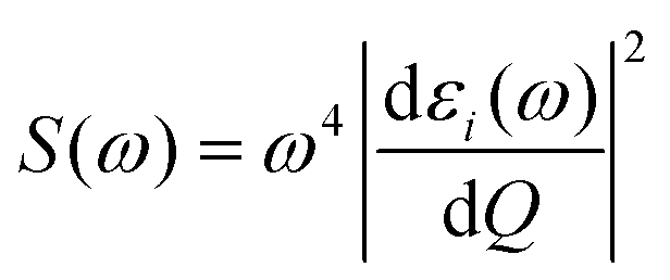
The efficiency of a Raman process for scattering by an optical phonon is proportional to the derivative of the dielectric tensor elements with respect to the normal coordinate of the phonon, Q. In particular we calculate the cross section, S(ω) which is defined as:
We compute the efficiency of Raman processes using a frozen phonon approach. We use the eigenmodes of the A1 and E2 zone-center phonons of WSe2 to determine the derivative of the in-plane dielectric function with the displacements of the normal phonon modes Q. The amplitude of the displacements were chosen to be small; the maximum atomic displacement was lower than 5% of the nearest neighbor W–Se bond length. The imaginary part of the dielectric function was calculated using a 28 × 28 × 1 k-point grid using tetrahedron integration with spin–orbit interaction included. Calculations using a 32 × 32 × 1 k-point grid lead to differences in the dielectric function on the order of 1 cm−1. Excitonic interactions were not considered.
Conflicts of interest
There are no conflicts of interest to declare.Acknowledgements
This work was supported by core programs at NRL and the NRL Nanoscience Institute. Computational work was supported by a grant of computer time from the DoD High Performance Computing Modernization Program at the US Army Research Laboratory Supercomputing Resource Center.Notes and references
- K. F. Mak, C. Lee, J. Hone, J. Shan and T. F. Heinz, Atomically Thin MoS2: A New Direct-Gap Semiconductor, Phys. Rev. Lett., 2010, 105(13), 136805 CrossRef PubMed.
- A. Splendiani, L. Sun, Y. Zhang, T. Li, J. Kim, C.-Y. Chim, G. Galli and F. Wang, Emerging Photoluminescence in Monolayer MoS2, Nano Lett., 2010, 10(4), 1271–1275, DOI:10.1021/nl903868w.
- B. Radisavljevic, A. Radenovic, J. Brivio, V. Giacometti and A. Kis, Single-Layer MoS2 Transistors, Nat. Nanotechnol., 2011, 6(3), 147–150, DOI:10.1038/nnano.2010.279.
- O. Lopez-Sanchez, D. Lembke, M. Kayci, A. Radenovic and A. Kis, Ultrasensitive Photodetectors Based on Monolayer MoS2, Nat. Nanotechnol., 2013, 8(7), 497–501 CrossRef CAS.
- F. K. Perkins, A. L. Friedman, E. Cobas, P. M. Campbell, G. G. Jernigan and B. T. Jonker, Chemical Vapor Sensing with Monolayer MoS2, Nano Lett., 2013, 13(2), 668–673, DOI:10.1021/nl3043079.
- M. R. Rosenberger, C. K. Dass, H.-J. Chuang, S. V. Sivaram, K. M. McCreary, J. R. Hendrickson and B. T. Jonker, Quantum Calligraphy: Writing Single-Photon Emitters in a Two-Dimensional Materials Platform, ACS Nano, 2019, 13(1), 904–912, DOI:10.1021/acsnano.8b08730.
- J.-H. Lee, J. Y. Park, E. B. Cho, T. Y. Kim, S. A. Han, T.-H. Kim, Y. Liu, S. K. Kim, C. J. Roh, H.-J. Yoon, H. Ryu, W. Seung, J. S. Lee, J. Lee and S.-W. Kim, Reliable Piezoelectricity in Bilayer WSe2 for Piezoelectric Nanogenerators, Adv. Mater., 2017, 29(29), 1606667, DOI:10.1002/adma.201606667.
- A. M. Jones, H. Yu, J. S. Ross, P. Klement, N. J. Ghimire, J. Yan, D. G. Mandrus, W. Yao and X. Xu, Spin–Layer Locking Effects in Optical Orientation of Exciton Spin in Bilayer WSe2, Nat. Phys., 2014, 10(2), 130, DOI:10.1038/nphys2848.
- Z.-Q. Xu, Y. Zhang, Z. Wang, Y. Shen, W. Huang, X. Xia, W. Yu, Y. Xue, L. Sun, C. Zheng, Y. Lu, L. Liao and Q. Bao, Atomically Thin Lateral p–n Junction Photodetector with Large Effective Detection Area, 2D Mater., 2016, 3(4), 041001, DOI:10.1088/2053-1583/3/4/041001.
- H. C. P. Movva, A. Rai, S. Kang, K. Kim, B. Fallahazad, T. Taniguchi, K. Watanabe, E. Tutuc and S. K. Banerjee, High-Mobility Holes in Dual-Gated WSe2 Field-Effect Transistors, ACS Nano, 2015, 9(10), 10402–10410, DOI:10.1021/acsnano.5b04611.
- E. del Corro, H. Terrones, A. Elias, C. Fantini, S. Feng, M. A. Nguyen, T. E. Mallouk, M. Terrones and M. A. Pimenta, Excited Excitonic States in 1L, 2L, 3L, and Bulk WSe2 Observed by Resonant Raman Spectroscopy, ACS Nano, 2014, 8(9), 9629–9635, DOI:10.1021/nn504088g.
- W. Zhao, Z. Ghorannevis, L. Chu, M. Toh, C. Kloc, P.-H. Tan and G. Eda, Evolution of Electronic Structure in Atomically Thin Sheets of WS2 and WSe2, ACS Nano, 2013, 7(1), 791–797, DOI:10.1021/nn305275h.
- Z. Gao, M.-Q. Zhao, M. M. A. Ashik and A. T. C. Johnson, Recentadvances in the Propertiesand Synthesis of Bilayer Graphene and Transition Metal Dichalcogenides, JPhys Mater., 2020, 3(4), 042003, DOI:10.1088/2515-7639/abb58d.
- Z. Zhang, Y. Liu, C. Dai, X. Yang, P. Chen, H. Ma, B. Zhao, R. Wu, Z. Huang, D. Wang, M. Liu, Y. Huangfu, S. Xin, J. Luo, Y. Wang, J. Li, B. Li and X. Duan, Highly Selective Synthesis of Monolayer or Bilayer WSe2 Single Crystals by Pre-Annealing the Solid Precursor, Chem. Mater., 2021, 33(4), 1307–1313, DOI:10.1021/acs.chemmater.0c04210.
- S. V. Mandyam, M.-Q. Zhao, P. M. Das, Q. Zhang, C. C. Price, Z. Gao, V. B. Shenoy, M. Drndić and A. T. C. Johnson, Controlled Growth of Large-Area Bilayer Tungsten Diselenides with Lateral P–N Junctions, ACS Nano, 2019, 13(9), 10490–10498, DOI:10.1021/acsnano.9b04453.
- P. Merkl, F. Mooshammer, S. Brem, A. Girnghuber, K.-Q. Lin, L. Weigl, M. Liebich, C.-K. Yong, R. Gillen, J. Maultzsch, J. M. Lupton, E. Malic and R. Huber, Twist-Tailoring Coulomb Correlations in van Der Waals Homobilayers, Nat. Commun., 2020, 11(1), 2167, DOI:10.1038/s41467-020-16069-z.
- A. Arora, P. K. Nayak, T. Dixit, K. L. Ganapathi, A. Krishnan and M. S. R. Rao, Stacking Angle Dependent Multiple Excitonic Resonances in Bilayer Tungsten Diselenide, Nanophotonics, 2020, 9(12), 3881–3887, DOI:10.1515/nanoph-2020-0034.
- J. J. Schwartz, H.-J. Chuang, M. R. Rosenberger, S. V. Sivaram, K. M. McCreary, B. T. Jonker and A. Centrone, Chemical Identification of Interlayer Contaminants within van Der Waals Heterostructures, ACS Appl. Mater. Interfaces, 2019, 11(28), 25578–25585, DOI:10.1021/acsami.9b06594.
- K. M. McCreary, A. T. Hanbicki, G. G. Jernigan, J. C. Culbertson and B. T. Jonker, Synthesis of Large-Area WS2 Monolayers with Exceptional Photoluminescence, Sci. Rep., 2016, 6, 19159, DOI:10.1038/srep19159.
- K. M. McCreary, A. T. Hanbicki, S. Singh, R. K. Kawakami, G. G. Jernigan, M. Ishigami, A. Ng, T. H. Brintlinger, R. M. Stroud and B. T. Jonker, The Effect of Preparation Conditions on Raman and Photoluminescence of Monolayer WS2, Sci. Rep., 2016, 6, 35154, DOI:10.1038/srep35154.
- Z. Liu, M. Amani, S. Najmaei, Q. Xu, X. Zou, W. Zhou, T. Yu, C. Qiu, A. G. Birdwell, F. J. Crowne, R. Vajtai, B. I. Yakobson, Z. Xia, M. Dubey, P. M. Ajayan and J. Lou, Strain and Structure Heterogeneity in MoS2 Atomic Layers Grown by Chemical Vapour Deposition, Nat. Commun., 2014, 5, 5246 CrossRef PubMed.
- A. T. Hanbicki, H.-J. Chuang, M. R. Rosenberger, C. S. Hellberg, S. V. Sivaram, K. M. McCreary, I. I. Mazin and B. T. Jonker, Double Indirect Interlayer Exciton in a MoSe2/WSe2 van Der Waals Heterostructure, ACS Nano, 2018, 12(5), 4719–4726, DOI:10.1021/acsnano.8b01369.
- A. M. van der Zande, P. Y. Huang, D. A. Chenet, T. C. Berkelbach, Y. You, G.-H. Lee, T. F. Heinz, D. R. Reichman, D. A. Muller and J. C. Hone, Grains and Grain Boundaries in Highly Crystalline Monolayer Molybdenum Disulphide, Nat. Mater., 2013, 12(6), 554–561 CrossRef CAS PubMed.
- E. P. dos Santos, F. L. R. Silva, R. N. Gontijo, J. M. Alves, M.-R. Ammar and C. Fantini, Temperature Dependence of the Double-Resonance Raman Bands in Bilayer WSe2, Vib. Spectrosc., 2020, 110, 103117, DOI:10.1016/j.vibspec.2020.103117.
- M. De Luca, X. Cartoixà, J. Martín-Sánchez, M. López-Suárez, R. Trotta, R. Rurali and I. Zardo, New Insights in the Lattice Dynamics of Monolayers, Bilayers, and Trilayers of WSe2 and Unambiguous Determination of Few-Layer-Flakes’ Thickness, 2D Mater., 2020, 7(2), 025004, DOI:10.1088/2053-1583/ab5dec.
- M. O'Brien, N. McEvoy, D. Hanlon, T. Hallam, J. N. Coleman and G. S. Duesberg, Mapping of Low-Frequency Raman Modes in CVD-Grown Transition Metal Dichalcogenides: Layer Number, Stacking Orientation and Resonant Effects, Sci. Rep., 2016, 6(1), 19476, DOI:10.1038/srep19476.
- K.-Q. Lin, J. Holler, J. M. Bauer, P. Parzefall, M. Scheuck, B. Peng, T. Korn, S. Bange, J. M. Lupton and C. Schüller, Large-Scale Mapping of Moiré Superlattices by Hyperspectral Raman Imaging, Adv. Mater., 2021, 33(34), 2008333, DOI:10.1002/adma.202008333.
- Y. Li, A. Chernikov, X. Zhang, A. Rigosi, H. M. Hill, A. M. van der Zande, D. A. Chenet, E.-M. Shih, J. Hone and T. F. Heinz, Measurement of the Optical Dielectric Function of Monolayer Transition-Metal Dichalcogenides: MoS2, MoSe2, WS2, and WSe2, Phys. Rev. B: Condens. Matter Mater. Phys., 2014, 90(20), 205422, DOI:10.1103/PhysRevB.90.205422.
- R. Frisenda, Y. Niu, P. Gant, A. J. Molina-Mendoza, R. Schmidt, R. Bratschitsch, J. Liu, L. Fu, D. Dumcenco, A. Kis, D. P. D. Lara and A. Castellanos-Gomez, Micro-Reflectance and Transmittance Spectroscopy: A Versatile and Powerful Tool to Characterize 2D Materials, J. Phys. D: Appl. Phys., 2017, 50(7), 074002, DOI:10.1088/1361-6463/aa5256.
- R. Schmidt, I. Niehues, R. Schneider, M. Drüppel, T. Deilmann, M. Rohlfing, S. M. Vasconcellos, A. de Castellanos-Gomez and R. Bratschitsch, Reversible Uniaxial Strain Tuning in Atomically Thin WSe2, 2D Mater., 2016, 3(2), 021011, DOI:10.1088/2053-1583/3/2/021011.
- A. Carvalho, R. M. Ribeiro and A. H. Castro Neto, Band Nesting and the Optical Response of Two-Dimensional Semiconducting Transition Metal Dichalcogenides, Phys. Rev. B: Condens. Matter Mater. Phys., 2013, 88(11), 115205, DOI:10.1103/PhysRevB.88.115205.
- R. Gillen and J. Maultzsch, Light-Matter Interactions in Two-Dimensional Transition Metal Dichalcogenides: Dominant Excitonic Transitions in Mono- and Few-Layer MoX2 and Band Nesting, IEEE J. Sel. Top. Quantum Electron., 2017, 23(1), 219–230, DOI:10.1109/JSTQE.2016.2604359.
- S. Kim, K. Kim, J.-U. Lee and H. Cheong, Excitonic Resonance Effects and Davydov Splitting in Circularly Polarized Raman Spectra of Few-Layer WSe 2, 2D Mater., 2017, 4(4), 045002, DOI:10.1088/2053-1583/aa8312.
- F. Cadiz, E. Courtade, C. Robert, G. Wang, Y. Shen, H. Cai, T. Taniguchi, K. Watanabe, H. Carrere, D. Lagarde, M. Manca, T. Amand, P. Renucci, S. Tongay, X. Marie and B. Urbaszek, Excitonic Linewidth Approaching the Homogeneous Limit in MoS2-Based van Der Waals Heterostructures, Phys. Rev. X, 2017, 7(2), 021026, DOI:10.1103/PhysRevX.7.021026.
- M. R. Rosenberger, H.-J. Chuang, K. M. McCreary, A. T. Hanbicki, S. V. Sivaram and B. T. Jonker, Nano-“Squeegee” for the Creation of Clean 2D Material Interfaces, ACS Appl. Mater. Interfaces, 2018, 10(12), 10379–10387, DOI:10.1021/acsami.8b01224.
- A. Ramasubramaniam, D. Naveh and E. Towe, Tunable Band Gaps in Bilayer Transition-Metal Dichalcogenides, Phys. Rev. B: Condens. Matter Mater. Phys., 2011, 84(20), 205325, DOI:10.1103/PhysRevB.84.205325.
- J. Kang, S. Tongay, J. Zhou, J. Li and J. Wu, Band Offsets and Heterostructures of Two-Dimensional Semiconductors, Appl. Phys. Lett., 2013, 102(1), 012111, DOI:10.1063/1.4774090.
- W.-T. Hsu, B.-H. Lin, L.-S. Lu, M.-H. Lee, M.-W. Chu, L.-J. Li, W. Yao, W.-H. Chang and C.-K. Shih, Tailoring Excitonic States of van Der Waals Bilayers through Stacking Configuration, Band Alignment, and Valley Spin, Sci. Adv., 2019, 5(12), eaax7407, DOI:10.1126/sciadv.aax7407.
- I. Paradisanos, S. Shree, A. George, N. Leisgang, C. Robert, K. Watanabe, T. Taniguchi, R. J. Warburton, A. Turchanin, X. Marie, I. C. Gerber and B. Urbaszek, Controlling Interlayer Excitons in MoS2 Layers Grown by Chemical Vapor Deposition, Nat. Commun., 2020, 11(1), 2391, DOI:10.1038/s41467-020-16023-z.
- Z. Gong, G.-B. Liu, H. Yu, D. Xiao, X. Cui, X. Xu and W. Yao, Magnetoelectric Effects and Valley-Controlled Spin Quantum Gates in Transition Metal Dichalcogenide Bilayers, Nat. Commun., 2013, 4(1), 2053, DOI:10.1038/ncomms3053.
- I. C. Gerber and X. Marie, Dependence of Band Structure and Exciton Properties of Encapsulated WSe2 Monolayers on the HBN-Layer Thickness, Phys. Rev. B, 2018, 98(24), 245126, DOI:10.1103/PhysRevB.98.245126.
- J. P. Perdew, K. Burke and M. Ernzerhof, Generalized Gradient Approximation Made Simple, Phys. Rev. Lett., 1996, 77(18), 3865–3868, DOI:10.1103/PhysRevLett.77.3865.
- P. E. Blöchl, Projector Augmented-Wave Method, Phys. Rev. B: Condens. Matter Mater. Phys., 1994, 50(24), 17953–17979, DOI:10.1103/PhysRevB.50.17953.
- G. Kresse and J. Hafner, Ab Initio Molecular Dynamics for Liquid Metals, Phys. Rev. B: Condens. Matter Mater. Phys., 1993, 47(1), 558–561, DOI:10.1103/PhysRevB.47.558.
- G. Kresse and J. Furthmüller, Efficient Iterative Schemes for Ab Initio Total-Energy Calculations Using a Plane-Wave Basis Set, Phys. Rev. B: Condens. Matter Mater. Phys., 1996, 54(16), 11169–11186, DOI:10.1103/PhysRevB.54.11169.
- S. Grimme, J. Antony, S. Ehrlich and H. Krieg, A Consistent and Accurate Ab Initio Parametrization of Density Functional Dispersion Correction (DFT-D) for the 94 Elements H-Pu, J. Chem. Phys., 2010, 132(15), 154104, DOI:10.1063/1.3382344.
Footnote |
| † Electronic supplementary information (ESI) available. See DOI: 10.1039/d1nr06119d |
| This journal is © The Royal Society of Chemistry 2022 |