
Transition-metal nitride halide dielectrics for transition-metal dichalcogenide transistors†
Mehrdad
Rostami Osanloo
 a,
Ali
Saadat
b,
Maarten L.
Van de Put
b,
Akash
Laturia
b and
William G.
Vandenberghe
*b
a,
Ali
Saadat
b,
Maarten L.
Van de Put
b,
Akash
Laturia
b and
William G.
Vandenberghe
*b
aDepartment of Physics, The University of Texas at Dallas, Richardson, TX 75080, USA
bDepartment of Materials Science and Engineering, The University of Texas at Dallas, Richardson, TX 75080, USA. E-mail: william.vandenberghe@utdallas.edu
First published on 14th December 2021
Abstract
Using first-principles calculations, we investigate six transition-metal nitride halides (TMNHs): HfNBr, HfNCl, TiNBr, TiNCl, ZrNBr, and ZrNCl as potential van der Waals (vdW) dielectrics for transition metal dichalcogenide (TMD) channel transistors. We calculate the exfoliation energies and bulk phonon energies and find that the six TMNHs are exfoliable and thermodynamically stable. We calculate both the optical and static dielectric constants in the in-plane and out-of-plane directions for both monolayer and bulk TMNHs. In monolayers, the out-of-plane static dielectric constant ranges from 5.04 (ZrNCl) to 6.03 (ZrNBr) whereas in-plane dielectric constants range from 13.18 (HfNBr) to 74.52 (TiNCl). We show that the bandgap of TMNHs ranges from 1.53 eV (TiNBr) to 3.36 eV (HfNCl) whereas the affinity ranges from 4.01 eV (HfNBr) to 5.60 eV (TiNCl). Finally, we estimate the dielectric leakage current density of transistors with six TMNH bilayer dielectrics with five monolayer channel TMDs (MoS2, MoSe2, MoTe2, WS2, and WSe2). For p-MOS TMD channel transistors 25 out of 30 combinations have a smaller leakage current than hexagonal boron nitride (hBN), a well-known vdW dielectric. The smallest bilayer leakage current of 1.15 × 10⁻² A cm−2 is predicted for a p-MOS MoSe2 transistor with HfNCl as a gate dielectric. HfNBr, ZrNBr, and ZrNCl are also predicted to yield small leakage currents in certain p-MOS TMD transistors.
I. Introduction
Two Dimensional (2D) van der Waals (vdW) materials have attracted a huge amount of attention owing to their unique properties and numerous applications in a wide variety of research areas, such as electronics, optoelectronics, and spintronics.1–5 With the advent of graphene, the first 2D thermodynamically stable material, the electronic industry entered a new area of technological revolution. The search for other promising 2D-vdW materials has led to the discovery of the most reputable class of 2D layered materials, transition metal dichalcogenides (TMDs), with a chemical formula of MX2 (where M is a transition metal and X is a chalcogen) and opened a research avenue for their unique and unprecedented electronic and optical properties.6–8 It is now well established that monolayers (1L) of TMDs exhibit exceptional physical behaviour compared to their multilayer or bulk form, especially under tensile strain, defect engineering, band structure engineering, and/or electric field exposure.9–14 In this regard, TMDs have been featured as n-type and p-type channel materials, in combination with 2D dielectric materials, to produce high-performance thin-film transistors (TFTs).15–17 Despite several studies performed in this field, there are still numerous issues for transistors with TMD channels and 2D dielectrics which have not yet been properly addressed and required more investigations.Transition-metal nitride halides (TMNHs) with chemical formula MNX (where M is a metal, N is nitrogen, and X is a halogen) are a less explored type of 2D-vdW material with layered crystal structures bound by a weak vdW force between the layers.18,19 Similar to other vdW materials, TMNHs have a huge potential to be utilized in various applications. Among the TMNHs, group-IVB nitride halides are of great interest since they are environmentally friendly materials.20 Several studies have been done on layered TMNHs to investigate properties such as superconductivity,21,22 photocatalyst,20 energy storage capability,23 and electronic properties.24,25 Moreover, we can envision materials like HfNCl to be compatible with existing semiconductor technology since HfCl4 is a known Atomic Layer Deposition (ALD) precursor26,27 and nitrogen is omnipresent in semiconductor processing. While TMNH electronic transport properties are starting to be explored, another unexplored option is to use TMNHs as vdW dielectrics.
In general, to find a good vdW layered dielectric candidate, we need to consider four criteria: (i) stability: layered dielectric materials must be stable and exfoliable. (ii) Leakage current: dielectrics must be a good insulator possessing a reasonable dielectric-channel band offset exceeding 1 eV to diminish leakage current by tunnelling or thermionic emission. (iii) Equivalent Oxide thickness (EOT): a small EOT is desirable for the purpose of the device miniaturization.2,28–32 (iv) Defects: defects introduce new electronic states in the bandgap, such that charge trapped in defects alter the gate threshold voltage. The first three criteria are directly determined by materials properties while the fourth criterion is also heavily determined by experimental process conditions. Despite numerous studies on dielectric properties of vdW materials,2,33 the investigation for dielectric properties of TMNHs is missing.
In this work, we perform first-principles calculations, using density functional theory (DFT), to study the optical and static in-plane and out-of-plane dielectric properties of monolayer and bulk form of six TMNHs: HfNBr, HfNCl, TiNBr, TiNCl, ZrNBr, and ZrNCl. We calculate the TMNH exfoliation energies and phonon energies to investigate the thermal structural stability of TMNHs. We also calculate bandgaps, electron affinities, and EOTs for the TMNHs under study. Furthermore, we consider five very well-known TMDs (MoS2, MoSe2, MoTe2, WS2, and WSe2) and calculate their band energies by DFT. Finally, we compute the leakage current of p-MOS transistors with TMNHs as gate dielectrics and TMDs as channel materials. We find that the combination of the TMNH materials under study with TMDs has significant potential for applications in the next generation of p-MOS devices.
II. Results and discussion
Fig. 1 shows the side and top views of the atomic structure of the TMNHs under study. More details of the structures such as space group and crystal structure type are listed in Table S1 in the ESI.† The layered crystal structures of TMNHs are found in two different types, the α-form (TiNBr and TiNCl) with A–A stacking configuration and the β-form (HfNBr, HfNCl, ZrNBr, and ZrNCl) with A–B–C stacking configuration.45,46 The α-form of monolayer TiNBr and TiNCl is a FeOCl-like orthorhombic layered network which is composed of an outer halogen layer (Cl and Br) added to the Ti atoms. The β-form, however, is made up of honeycomb-like sheets of M–N layers crammed with halogen atoms. The β-form has a SmSI (samarium sulfide iodide) layer structure and is more stable in a hostile environment than the α-form.46 The β-form structures can stand hot acid solutions whereas the α-form structures are hydrolyzed in air.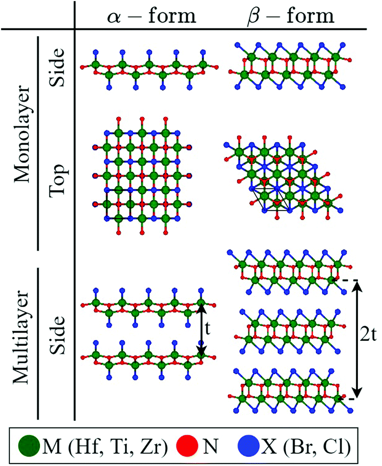 | ||
| Fig. 1 Structures of the TMNH materials, with chemical formula MNX, under study. The side view and top view of the monolayer in addition to the side view of the multilayer are illustrated. The α-form (A–A stacking configuration) represents TiNBr and TiNCl structures whereas the β-form (A–B–C stacking configuration) represents the structures of HfNBr, HfNCl, ZrNBr, and ZrNCl. The monolayer thickness (t) is indicated on the multilayer structures. | ||
The monolayer thickness of the TMNHs under study ranges from 7.88 Å (TiNCl) to 9.82 Å (HfNBr and ZrNBr). Structural parameters such as monolayer thickness (t), bulk interlayer distance (d), the percentage difference between d and t (Δ), and lattice constant (a) of all TMNHs under study are reported in Table S2 in the ESI.† The optimized monolayer lattice constants of the β-form monolayers range from 3.59 Å (HfNCl) to 3.65 Å (ZrNBr), whereas the α-form monolayer of TiNCl and TiNBr have lattice constants of 3.26 Å and 3.36 Å respectively. The calculated lattice constant values are in good agreement with experimental and theoretical values reported in other works.18,20
First, we calculate the exfoliation energies, Eex, to certify whether materials in this study are layered and can be produced from their bulk crystal counterparts. The exfoliation energy ranges from 15.55 meV Å−2 (TiNCl) to 18.95 meV Å−2 (HfNBr). All Eex values for TMNH materials are listed in Table S2.† As reported in ref. 47 materials with Eex < 100 meV Å−2 are deemed easily exfoliable compounds.
We note that ref. 47 reports binding energies and the band gap for ZrNCl and ZrNBr. However, ref. 47 considers only half of the monolayer structure of our study with the structure cleaved at the Zr–N bond yielding a 3-atom instead of a 6-atom monolayer unit cell in our work. We calculate that ref. 47's half monolayer has an exfoliation energy 85.82 eV cm−2 compared to 19.62 eV cm−2 for the current structure indicating that the monolayers we consider will be more easily realizable in an experimental setting.
According to Table S2,† all six TMNHs materials in this study have weak vdW interlayer interactions and are therefore exfoliable and layered. Moreover, to examine the stability of monolayers we calculate the phonon energies of monolayer and bulk for all TMNH materials. In the ESI,† we tabulate the monolayer and bulk form phonon energy values in Tables S3 and S4,† respectively. No significant imaginary phonon energies are observed indicating that all monolayer materials are stable.
In Table S5 in the ESI,† the x and y components are separately reported for the monolayer and bulk TMNH materials in this study showing the in-plane anisotropy of TiNBr and TiNCl.
Fig. 2 shows the calculated macroscopic in-plane (∥) and out-of-plane (⊥) dielectric constants for the materials under study. The values of the dielectric constants for all materials are listed in Table 1. While the optical dielectric constant (ε∞) only contains the electronic response, the static dielectric constant (ε0), on the other hand, includes both the ionic and the electronic contributions to the dielectric response. For the calculation of the dielectric constant of monolayer slabs, we first introduce an appropriate amount of vacuum size (at least 15 Å) to the computational supercell. Applying a sufficient vacuum size is critical to effectively isolate monolayers from other layers and counteract unwanted interlayer interactions. As recently presented in,2,33 we remove the vacuum effect by rescaling the supercell dielectric constants to those of the monolayer. For the in-plane dielectric calculation, we calculate the geometric mean over the x and y components of dielectric values. In Table S5 in the ESI,† the x and y components are separately reported for the monolayer and bulk TMNH materials in this study showing the in-plane anisotropy of TiNBr and TiNCl.
| Material | Monolayer (ε∞) | Monolayer (ε0) | Bulk (ε∞) | Bulk (ε0) | ||||
|---|---|---|---|---|---|---|---|---|
| ∥ | ⊥ | ∥ | ⊥ | ∥ | ⊥ | ∥ | ⊥ | |
| ZrNCl | 6.23 | 4.23 | 15.85 | 5.04 | 6.24 | 4.10 | 15.68 | 5.28 |
| HfNCl | 5.65 | 4.15 | 13.69 | 5.13 | 5.67 | 4.04 | 13.61 | 5.32 |
| TiNCl | 12.40 | 4.36 | 74.52 | 5.08 | 12.76 | 4.25 | 75.74 | 5.02 |
| ZrNBr | 6.69 | 4.97 | 15.30 | 6.03 | 6.72 | 4.86 | 14.87 | 6.08 |
| HfNBr | 6.10 | 4.84 | 13.18 | 5.94 | 6.12 | 4.70 | 13.16 | 6.04 |
| TiNBr | 13.10 | 5.14 | 67.01 | 5.76 | 13.37 | 4.95 | 68.22 | 5.65 |
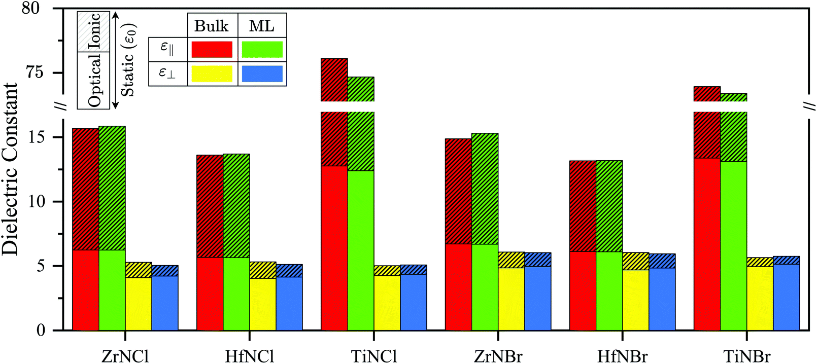 | ||
| Fig. 2 Dielectric constants for monolayer and bulk of the TMNHs. Both optical (ε∞) and static (ε0) dielectric constants in the in-plane (∥) and out-of-plane (⊥) directions are shown. Larger shaded area represents higher ionic contribution in dielectric constants. TiNBr and TiNCl have relatively high ionic response in their dielectric constants. All dielectric values are reported in Table 1. Only TiNBr and TiNCl are anisotropic materials, εx ≠ εy, (see Table S5†). | ||
For the bulk samples, Fig. 2 shows that TiNCl (75.74) and HfNBr (13.16) exhibit the highest and the lowest in-plane static dielectric constants, respectively, whereas ZrNBr (6.08) and TiNCl (5.02) display the highest and the lowest out-of-plane static dielectric constants, respectively. The in-plane static dielectric constants of TiNBr and TiNCl are approximately six times larger than the corresponding optical dielectric constants indicating that there is a significant ionic contribution to the dielectric response for TiNBr and TiNCl. The optical dielectric constants range from 5.67 (HfNCl) to 13.37 (TiNBr) in the in-plane direction and locate between 4.04 (HfNCl) and 4.95 (TiNBr) in the out-of-plane direction, respectively.
In monolayers, Fig. 2 reveals that the highest and the lowest in-plane static dielectric constants are attributed to TiNCl (74.52) and HfNBr (13.18), respectively. In addition, the out-of-plane static dielectric constants lie between 5.04 for ZrNCl and 6.03 for ZrNBr. Similar to the bulk structures, the ionic contribution of TiNBr and TiNCl to the in-plane dielectric responses are noticeably high. For the optical dielectric constants, HfNCl has the lowest in-plane (5.65) and out-of-plane (4.15) dielectric constants whereas, TiNBr has the highest in-plane (13.10) and out-of-plane (5.14) dielectric constants.
There is a small difference between the dielectric constant values of monolayer and bulk in both in-plane and out-of-plane directions. Going from bulk to monolayer, we observe that the in-plane optical dielectric constants decrease less than 3%, while the out-of-plane optical response increases by up to 4%. Similar to the in-plane optical dielectric constants, the in-plane static dielectric constants show less than 3% difference between bulk and monolayer dielectric constants. However, by moving from bulk to monolayer we detect an increase in the in-plane dielectric constant for ZrNCl, HfNCl, ZrNBr, and HfNBr whereas, the trend is the opposite for TiNBr and TiNCl, such that their dielectric constants decrease marginally. For the out-of-plane static dielectric constants, the maximum difference is exhibited by ZrNCl with an increase of 4.8% going from monolayer to bulk.
Fig. 3 shows the energy band alignment of the TMNH materials, hBN, and TMDs. We calculate the electron affinity, bandgap, and conduction-valence band edges of TMNHs and TMDs to analyze the insulating properties of TMNHs for transistors with TMD channel materials. We report the bandgap and the electron affinity (difference between the vacuum level and the conduction band minimum) values of the TMNHs and TMDs on Fig. 3. We also add hBN, a very well-known 2D gate dielectric to our figure for the purpose of comparison. The green and yellow bars respectively show the conduction, and the valence band positions relative to the vacuum reference, which is set at zero. The monolayer bandgap and electron affinity values of all materials in this study are calculated by Heyd–Scuseria–Ernzerhof (HSE06) hybrid functional method to correct for bandgap underestimation. The underestimated Perdew–Burke–Ernzerof (PBE) values of TMNHs are provided in Table S6 in the ESI.†
 | ||
| Fig. 3 Band alignment of TMNHs. Top bars (green) and bottom bars (yellow) show conduction band and valence band energies, respectively. The bandgap and electron affinity values of each TMNH are indicated on the figure (Table S6 in the ESI†). hBN is added for the purpose of comparison (Table S7 in the ESI†). The band alignment of TMDs, showing the bandgap and electron affinity values (in parenthesis), are placed on the right side of the figure as guides to the eye. | ||
As a general principle, a suitable dielectric candidate should possess a band offset exceeding 1 eV with the channel material to efficiently minimize leakage current.48 Our calculation shows that none of TMNHs in our list are good candidate dielectrics for n-MOS TMD applications because of the small TMNH-TMD offset which would result in an unacceptably high dielectric leakage current. However, there are promising TMNH dielectric materials for p-MOS transistors owing to a sufficiently large bandgap and favorable band offset with respect to the TMD channel materials. Furthermore, Fig. 3 shows that all TMNH materials and hBN have a similar valence band edge and promise performance similar to hBN.
We calculate the EOT values for monolayer and bilayer (2L) of all six TMNH dielectric materials and plot the results in Fig. 4. We add monolayer and bilayer hBN, reported in ref. 33, for the purpose of comparison. For the monolayer EOT (narrow bars), we consider the monolayer thickness from Table S2† and the monolayer out-of-plane static dielectric constant from Table 1. For the bilayer EOT (wide bars) we present a range between two different assumptions: one where the bilayer has the dielectric constant of the monolayer and one where the bilayer has the dielectric constant of the bulk. We assume the bilayer thickness equals twice the monolayer thickness. The shaded area for each TMNH shows the range the bilayer EOT lies in, the shaded area is small indicating that both assumptions for bilayer dielectric constant yield similar results.
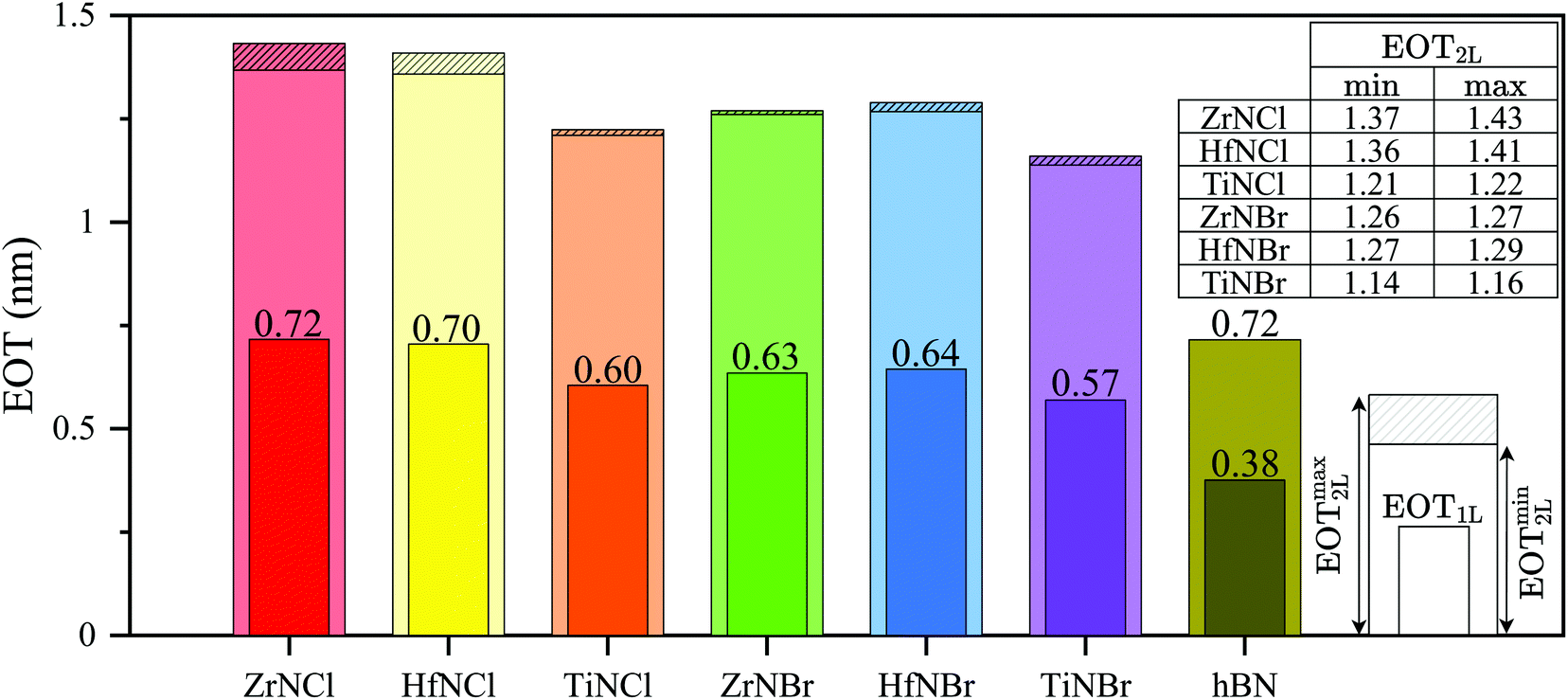 | ||
| Fig. 4 Monolayer (narrow bars) and bilayer (wide bars) EOT for the TMNHs under study. Monolayer EOT is calculated from monolayer out-of-plane static dielectric constants and monolayer thickness. Bilayer EOT is calculated at two extremes assuming the bilayer dielectric constant either equals the monolayer or the bulk out-of-plane static dielectric constants. In the inset, two extreme values of bilayer EOT for gate dielectrics are reported. hBN values are calculated from the hBN dielectric constant and thickness for monolayer and bilayer, as reported in ref. 31. | ||
Monolayer EOT values of TMNH materials in this study range from 0.57 nm (TiNBr) to 0.72 nm (ZrNCl) as shown in Fig. 4. Our results show we can benefit from ultrathin 1 nm EOT in all materials that can subjugate short-channel effects and compete with other 2D layered ultrathin dielectric materials. Taking only EOT into account, monolayer hBN with an EOT of 0.38 nm outperforms the TMNHs investigated here. However, monolayer hBN leakage currents are known to be unacceptable in CMOS technology.49
We also determine the leakage current density of TMNHs. Fig. 5 shows the dielectric leakage current of p-MOS transistors with the six bilayer TMNHs under study in combination with five well-known TMDs, yielding 30 combinations in total. We add four-layer (4L) hBN for the purpose of comparison. The leakage current includes three components: thermionic emission, direct tunneling current through the valence band, and direct tunnelling current through the conduction band.
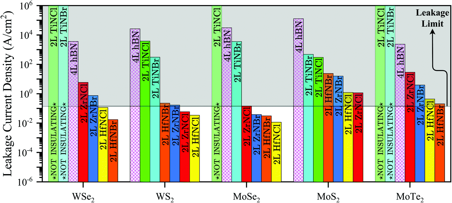 | ||
| Fig. 5 Leakage current of p-MOS transistors with six bilayer TMNHs under study in combination with five well-known TMDs. 4L hBN is added for the purpose of comparison. Only 7 out of 30 combinations (HfNBr/HfNCl/ZrNBr when they are combined with MoSe2, HfNCl/ZrNCl when they are combined with WS2, and HfNBr/HfNCl when they are combined with WSe2) have a sufficiently low leakage current. The shaded area indicates unaccepted leakage currents, i.e. exceeding the leakage current limit according to IRDS.39 | ||
We report the leakage current values for each component as well as the total leakage current values in Table S8 in the ESI.† The thermionic current is relatively negligible for all materials whereas the tunneling currents are dominant. More details about the leakage current calculation are provided in the method section. For each TMD channel material, TMNH materials with bars on the right side of the hBN bar outperform 4L hBN. 25 combinations have a smaller leakage current than hBN. The smallest leakage current of 1.15 × 10⁻² A cm−2 is predicted for a WSe2 p-MOS transistor with bilayer HfNCl. 7 out of 30 combinations (HfNCl/HfNBr/ZrNBr when combined with MoSe2, HfNCl/ZrNCl when combined with WS2, and HfNBr/HfNBr when combined with WSe2) sufficiently insulate current to meet the IRDS specification. In addition, 2L TiNCl and TiNBr are not suitable insulators when combined with WSe2, MoSe2, and MoTe2.
According to the 2020 IRDS,43 a maximum leakage current of 100 pA μm−1 needs to be considered for any viable gate dielectric. Assuming a 28 nm pitch, an 18 nm long gate, and an effective gate with of 107 nm, the acceptable leakage current density becomes 0.145 A cm−2. The shaded area on Fig. 5 shows the unaccepted leakage current density based on IRDS criteria. Among the 30 combinations of 2L TMNHs and TMDs proposed in this study, 7 combinations result in a leakage current smaller than the limit, 0.145 A cm−2. Among the five TMDs, MoSe2, WS2, and WSe2 are the most promising channel materials in terms of leakage current since their combination with four 2L TMNHs (HfNBr, HfNCl, ZrNBr, and ZrNCl), yields p-MOS transistors with acceptable leakage currents. On the other hand, the combination of MoTe2 and MoSe2 with all six 2L TMNHs result in unacceptable leakage currents. Moreover, the leakage current of TiNBr, TiNCl, and hBN with all five TMDs exceed the leakage current limit. As depicted in Fig. 5, even 4L h-BN has worse performance for p-MOS when combined with the 6 TMDs under consideration. We calculate that at least 7 layers of hBN (EOT = 2.30 nm) on WSe2 and MoTe2, 9 layers of hBN (EOT = 2.96 nm) on WS2 and MoS2, and 11 layers of hBN (EOT = 3.62 nm) on MoS2 are needed to prevent exceeding the leakage current limit. However, considering another proposed leakage current limit suitable for low-power applications48 excludes six more combinations and results in one acceptable combination: MoSe2 when it is combined with HfNCl. On the other hand, computing the leakage of three layers of the TMNHs on all TMDs, we observe that 3L HfNCl, HfNBr, ZrNCl, and ZrNBr always meet the leakage current criterion.
The excessive leakage current of hBN with all five TMDs, showing in Fig. 5, is in good agreement with a recent finding by Knobloch et al. in ref. 49,50. Knobloch et al. performed theoretical work, using DFT, and experimental work, using Chemical Vapor Deposition (CVD) and exfoliation of hBN, and reported that hBN is unlikely to be suitable for ultrascaled CMOS transistors due to excessive leakage current. Knobloch et al. used trilayer hBN as a gate insulator on p-type silicon and calculated leakage current revealing that the leakage current of devices with hBN exceeds the low-power limit, however, when the operating when the voltage drops over the oxide is lower than 0.5 V, hBN trilayers could be used. In another recent study,2 it was shown that hBN leakage current is larger than the leakage current limit determined by IRDS. Finally, we note that recently six monolayer 2D halide dielectrics (HoOI, LaOBr, LaOCl, LaOI, SrI2, and YOBr), suitable for n-MOS applications, have been proposed in ref. 2 to outperform hBN and HfO2.
Moreover, we report the monolayer bandgap, electron affinity and polarizability of TMNH dielectrics and compare our results with other works35 in Table S9 of the ESI.† In addition, since the lattice mismatch could be a critical factor during fabrication process, we report the lattice mismatch between the proposed TMNH dielectrics and TMD channels in Table S10 of the ESI.† According to our calculation the smallest lattice mismatch is exhibited by TiNCl combined with WSe2, WS2, MoS2, and MoSe2 and HfNCl combined with MoTe2.
III. Methods
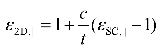
To perform our calculations, we obtain our primary input file including atomic positions of materials from Materials Project34 and use DFT as implemented in the Vienna ab initio simulation package (VASP).36 For the electron exchange and correlation functional we employ the generalized gradient approximation (GGA) as proposed by Pedrow–Burke–Ernzerof (PBE).37 To ensure accuracy we set the plane wave extension energy cut-off of 520 eV for TMNHs, and structural relaxations are performed until the force on each atom is less than 10−3 eV Å−1. To achieve accurate dielectric constants, we set a strict energy convergence criterion of 10−8 eV. For monolayer TMDs in this paper, we use the plane wave energy cut-off range between 450 eV to 520 eV and set an energy break condition for the electronic self-consistency loop and ionic relaxation loop to 10−5 eV and 10−4 eV, respectively. To sample the Brillouin Zone (BZ), 15 × 15 × 3 (9 × 9 × 9) and 15 × 15 × 1 (9 × 9 × 1) Gamma k-point grids are adopted for the bulk and the monolayer structures of HfNBr, HfNCl, ZrNBr, ZrNCl (TiNBr, TiNCl), respectively. To account for the interlayer van der Waals interactions, we use the DFT-D3 method of Grimme.38 We also apply at least 15 Å vacuum barrier to the monolayer cells to avoid any possible interactions between layers. Furthermore, the exfoliation energy is computed as the ratio between the difference between the ground state energies of bulk and monolayers to the bulks’ surface area.39,40 To avoid underestimating the band gap, we use the Heyd–Scuseria–Ernzerhof (HSE06) functional for both band gap and electron affinity calculations. To obtain the band alignment we use Anderson's rule. For monolayer TMD band gaps, we perform HSE06 calculations including spin–orbit coupling (SOC) interactions with 5 × 5 × 1 k-point mesh sampling in the first BZ. After determining the ground state on the 5 × 5 × 1 mesh, we add two 25-point path along the Γ → M and Γ → K directions to ensure we capture the band minimum/maximum.To calculate the bulk dielectric constants, we use Density Functional Perturbation Theory (DFPT), implemented in VASP, computing the permittivity tensor of the bulk unit cell. From the permittivity tensor, we derive the in-plane dielectric constant by calculating the geometric mean over the x and y components, 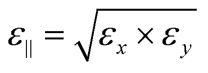 , and consider the third component for the out-of-plane dielectric constant, ε⊥ = εz. We calculate the optical dielectric constant (ε∞) at high frequency where only the electrons respond to the external field and the ions remain frozen in their positions. To account for the ionic response, we compute the static dielectric constant (ε0) which includes both the electronic and ionic responses. To analyze the monolayer dielectric constant, we need to remove the vacuum contribution from the supercell dielectric values and rescale the supercell dielectric constants. Following ref. 2 and 33, we rescale the supercell dielectric constants using the following equations:
 | (1) |
 | (2) |
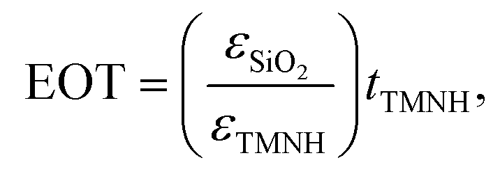
To calculate the EOT, we use
 | (3) |
Dielectric leakage current through the metal–semiconductor is calculated by considering three components: thermionic emission over the barriers (φ = [χTMNH + Eg,TMNH] – [χTMD + Eg,TMD], where χ is the electron affinity and Eg is the bandgap), tunneling current through the valence band (φ = [χTMNH + Eg,TMNH] – [χTMD + Eg,TMD]), and tunneling current through the conduction band (φ = [χTMD + Eg,TMD] − χTMNH). The following equations are used to obtain the thermionic and direct tunneling current densities:41,42,51
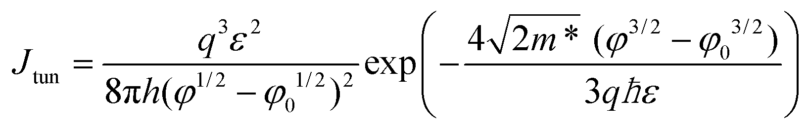 | (4) |
 | (5) |
To calculate the leakage current, we use the VDD = 0.7 V supply voltage and Vt = 0.345 V threshold voltage as introduced in the 2020 International Roadmap for Devices and Systems (IRDS).43 The electric field inside the insulator, ε, is calculated using  . Since the band structures of the TMNHs are flat along the out-of-plane direction, we use the free hole mass for the tunneling calculations (m* = mh). The hBN hole effective mass, 0.47mh, is taken from ref. 44. For the thermionic emission calculation, we use the out-of-plane static dielectric constants. The monolayer thickness of materials is used for leakage current calculations. A temperature of 300 K is assumed.
IV. Conclusions
We investigated TMNH layered dielectric materials which are classified into two forms (α-form and β-form) based on their lattice structures and space groups. We carried out first-principles calculations to accurately compute in-plane and out-of-plane optical and static dielectric constants for the bulk and monolayers of six TMNHs. The monolayer in-plane static dielectric constant of monolayer TiNCl and TiNBr were shown to be much greater than the other materials, whereas the out-of-plane static dielectric constant for all materials is in the same range, where ZrNBr has the largest dielectric constant. We calculated phonon and exfoliation energies proving that all TMNH bulk materials are thermodynamically stable and potentially exfoliable down to monolayers. We also estimated monolayer HSE bandgap values, electron affinities, and band edges for TMNH materials and TMD channels.To investigate the potential of materials under study for p-MOS applications, we calculated EOT and leakage current of transistors with TMNHs as gate dielectrics and TMDs as channels materials. All six 2L TMNHs have an EOT < 1.5 nm suitable for ultrascaled CMOS devices. We found that 4L hBN has excessive leakage current with all five TMDs. Among the 30 combinations (six TMNHs and five TMDs), 25 combinations showed a smaller leakage current than hBN while 7 combinations have a leakage current smaller than the low-power limit introduced by IRDS. The combination of 2L HfNCl with MoSe2 has the smallest leakage current density (1.15 × 10⁻² A cm−2). WSe2, WS2, and MoSe2 were found as the most promising TMDs in this study since their combination with four 2L TMNHs (HfNBr, HfNCl, and ZrNBr) resulted in relatively low leakage currents. TiNBr and TiNCl with all five TMDs result in large leakage currents exceeding the leakage current limit defined by IRDS. Based on our findings, we propose four promising 2D gate dielectrics (HfNBr, HfNCl, and ZrNBr) most suited for ultrascaled TMD p-MOS transistors.
TMNHs cannot be used as dielectrics for n-MOS applications but have the advantage that they are composed of elements that are well established in the semiconductor industry. When a solution for both n-and p-MOS is required, materials based on rare-earth elements like LaOCl, previously identified in ref. 2, are good candidates.
Our approach can be used to discover more 2D gate dielectric materials and investigate the performance of novel ultrascaled CMOS devices.
Conflicts of interest
There are no conflicts to declare.Acknowledgements
This research was sponsored in part by the Semiconductor Research Corporation (SRC) under the Logic and Memory Devices (LMD) Program of the Global Research Collaboration (GRC).The project or effort depicted was or is sponsored by the Department of Defence, Defence Threat Reduction Agency. The content of the information does not necessarily reflect the position or the policy of the federal government, and no official endorsement should be inferred.
References
- D. L. Duong, S. J. Yun and Y. H. Lee, van der Waals layered materials: Opportunities and challenges, ACS Nano, 2017, 11(12), 11803–11830, DOI:10.1021/acsnano.7b07436.
- M. R. Osanloo, M. L. Van de Put, A. Saadat and W. G. Vandenberghe, Identification of Two-Dimensional Layered Dielectrics from First Principles, Nat. Commun., 2021, 12(1), 5051, DOI:10.1038/s41467-021-25310-2.
- Y. Liu, Y. Huang and X. Duan, van der Waals integration before and beyond two-dimensional materials, Nature, 2019, 567, 323–333, DOI:10.1038/s41586-019-1013-x.
- M. Wu and P. Jena, The rise of two-dimensional van der Waals ferroelectrics, Wiley Interdiscip. Rev.: Comput. Mol. Sci., 2018, 8(5), e1365, DOI:10.1002/wcms.1365.
- W. Hu and J. Yang, First-principles study of two-dimensional van der Waals heterojunctions, Comput. Mater. Sci., 2016, 112, 518–526, DOI:10.1016/j.commatsci.2015.06.033.
- S. Manzeli, D. Ovchinnikov, D. Pasquier, O. V. Yazyev and A. Kis, 2D transition metal dichalcogenides, Nat. Rev. Mater., 2017, 2(8), 1–15, DOI:10.1038/natrevmats.2017.33.
- A. Daus, et al., High-performance flexible nanoscale transistors based on transition metal dichalcogenides, Nat. Electron., 2021, 1–7, DOI:10.1038/s41928-021-00598-6.
- S. Fathipour, et al., Exfoliated multilayer MoTe2 field-effect transistors, Appl. Phys. Lett., 2014, 105(19), 192101, DOI:10.1063/1.4901527.
- I. V. Chepkasov, M. a. Ghorbani-Asl, Z. I. Popov, J. H. Smet and A. V. Krasheninnikov, Alkali metals inside bi-layer graphene and MoS 2 : Insights from first-principles calculations, Nano Energy, 2020, 75, 104927, DOI:10.1016/j.nanoen.2020.104927.
- A. Jalouli, M. Kilinc, P. Wang, H. Zeng and T. Thomay, Spatial mapping of exciton transition energy and strain in composition graded WS 2(1-x) Se 2x monolayer, J. Appl. Phys., 2020, 128(12), 124304, DOI:10.1063/5.0021361.
- S. Erfanifam, et al., Tunable bandgap and spin-orbit coupling by composition control of MoS 2 and MoO x (x = 2 and 3) thin film compounds, Mater. Des., 2017, 122, 220–225, DOI:10.1016/j.matdes.2017.02.085.
- W. Liu, et al., New Verbeekite-type polymorphic phase and rich phase diagram in the PdSe 2− x Te x system, Phys. Rev. B, 2021, 104(2), 024507, DOI:10.1103/PhysRevB.104.024507.
- K. Noori, N. L. Q. Cheng, F. Xuan and S. Y. Quek, Dielectric screening by 2D substrates, 2D Mater., 2019, 6(3), 035036, DOI:10.1088/2053-1583/ab1e06.
- K. T. Winther and K. S. Thygesen, Band structure engineering in van der Waals heterostructures via dielectric screening: the GΔW method, 2D Mater., 2017, 4(2), 025059, DOI:10.1088/2053-1583/aa6531.
- L. J. Stanley, et al., Low-Temperature 2D/2D Ohmic Contacts in WSe 2 Field-Effect Transistors as a Platform for the 2D Metal-Insulator Transition, ACS Appl. Mater. Interfaces, 2021, 10594–10602, DOI:10.1021/acsami.0c21440.
- B. Jiang, Z. Yang, X. Liu, Y. Liu and L. Liao, Interface engineering for two-dimensional semiconductor transistors, Nano Today, 2019, 25, 122–134, DOI:10.1016/j.nantod.2019.02.011.
- S. Das, R. Gulotty, A. V. Sumant and A. Roelofs, All Two-Dimensional, Flexible, Transparent, and Thinnest Thin Film Transistor, Nano Lett., 2014, 14, 2861–2866, DOI:10.1021/nl5009037.
- W. S. Yun and J. D. Lee, Two-dimensional semiconductors ZrNCl and HfNCl: Stability, electric transport, and thermoelectric properties, Sci. Rep., 2017, 7(1), 1–9, DOI:10.1038/s41598-017-17590-w.
- X. Deng, B. Luo, Z. Zhang, C. Zhao, M. Shi and E. Tian, Structural, electronic, and optical properties of two-dimensional hafnium monoxide nanosheets, Phys. E, 2021, 130, 114690, DOI:10.1016/j.physe.2021.114690.
- J. Liu, X.-B. Li, D. Wang, H. Liu, P. Peng and L.-M. Liu, Single-layer Group-IVB nitride halides as promising photocatalysts, J. Mater. Chem. A, 2014, 2(19), 6755–6761, 10.1039/C3TA15431A.
- Q. Yin, E. R. Ylvisaker and W. E. Pickett, Spin and charge fluctuations in α-structure layered nitride superconductors, Phys. Rev. B: Condens. Matter Mater. Phys., 2011, 83(1), 014509, DOI:10.1103/PhysRevB.83.014509.
- S. Zhang, M. Tanaka and S. Yamanaka, Superconductivity in electron-doped layered TiNCl with variable interlayer coupling, Phys. Rev. B: Condens. Matter Mater. Phys., 2012, 86(2), 024516, DOI:10.1103/PhysRevB.86.024516.
- X. Zhang, Z. Zhang, X. Zhao, D. Wu, X. Zhang and Z. Zhou, Tetragonal-structured anisotropic 2D metal nitride monolayers and their halides with versatile promises in energy storage and conversion, J. Mater. Chem. A, 2017, 5(6), 2870–2875, 10.1039/C6TA10980B.
- X. Liu, et al., Ab initio prediction of thermoelectric properties of monolayer ZrNCl and HfNCl, J. Solid State Chem., 2020, 290, 121500, DOI:10.1016/j.jssc.2020.121500.
- P. M. Woodward and T. Vogt, Electronic Band Structure Calculations of the MNX (M=Zr, Ti;X=Cl, Br, I) System and Its Superconducting Member, Li-Doped β-ZrNCl, J. Solid State Chem., 1998, 138(2), 207–219, DOI:10.1006/jssc.1997.7601.
- A. B. Mukhopadhyay, C. B. Musgrave and J. F. Sanz, Atomic Layer Deposition of Hafnium Oxide from Hafnium Chloride and Water, J. Am. Chem. Soc., 2008, 130(36), 11996–12006, DOI:10.1021/ja801616u.
- H. B. Park, M. Cho, J. Park, S. W. Lee and C. S. Hwang, Comparison of HfO2 films grown by atomic layer deposition using HfCl4 and H2O or O3 as the oxidant, J. Appl. Phys., 2003, 94(5), 3641–3647, DOI:10.1063/1.1599980.
- Y. Y. Illarionov, et al., Insulators for 2D nanoelectronics: the gap to bridge, Nat. Commun., 2020, 3385, DOI:10.1038/s41467-020-16640-8.
- R. M. Wallace, Dielectric materials for microelectronics, Springer handbook of electronic and photonic materials, Springer, Cham, 2017, p. 1, DOI:10.1007/978-3-319-48933-9_27.
- G. D. Wilk, R. M. Wallace and J. M. Anthony, High-κ gate dielectrics: Current status and materials properties considerations, J. Appl. Phys., 2001, 89(10) DOI:10.1063/1.1361065.
- L. Teitz and M. C. Toroker, Theoretical Investigation of Dielectric Materials for Two-Dimensional Field-Effect Transistors, Adv. Funct. Mater., 2019, 30(18), 1808544, DOI:10.1002/adfm.201808544.
- W. Chao and M. Lanza, Calcium fluoride as high-k dielectric for 2D electronics, Appl. Phys. Rev., 2021, 8(2), 021307, DOI:10.1063/5.0036987.
- A. Laturia, M. L. Van de Put and W. G. Vandenberghe, Dielectric properties of hexagonal boron nitride and transition metal dichalcogenides: from monolayer to bulk, npj 2D Mater. Appl., 2018, 2(1), 1–7, DOI:10.1038/s41699-018-0050-x.
- A. Jain, et al., Commentary: The Materials Project: A materials genome approach to accelerating materials innovation, APL Mater., 2013, 1(1), 011002, DOI:10.1063/1.4812323.
- M. N. Gjerding, et al., Recent progress of the computational 2D materials database (C2DB), 2D Mater., 2021, 8, 042002, DOI:10.1088/2053-1583/aacfc1.
- J. Heyd and G. E. Scuseria, Efficient hybrid density functional calculations in solids: Assessment of the Heyd–Scuseria–Ernzerhof screened Coulomb hybrid functional, J. Chem. Phys., 2004, 121, 1187–1192, DOI:10.1063/1.1760074.
- J. Perdew, K. Burke and M. Ernzerhof, Generalized Gradient Approximation Made Simple, Phys. Rev. Lett., 1996, 3865–3868, DOI:10.1103/PhysRevLett.77.3865.
- S. Grimme, Semiempirical GGA-type density functional constructed with a long-range dispersion correction, 2006. DOI:10.1002/jcc.20495.
- M. Ashton, et al., Topology-scaling identification of layered solids and stable exfoliated 2D materials, Phys. Rev. Lett., 2017, 118(10), 106101 CrossRef PubMed.
- T. Björkman, et al., van der Waals bonding in layered compounds from advanced density-functional first-principles calculations, Phys. Rev. Lett., 2012, 108(23), 235502 CrossRef PubMed.
- A. Gehring, 2012 Simulation of tunneling in semiconductor devices, Diss., 2003 Search PubMed.
- Y. C. Yeo, et al., Direct tunneling gate leakage current in transistors with ultrathin silicon nitride gate dielectric, IEEE Electron Device Lett., 2000, 21(11), 540–542, DOI:10.1109/55.877204.
- M. Moor, International Roadmap For Devices and Systems, 2020 Search PubMed.
- P. Palla, G. R. Uppu, A. S. Ethiraj and J. P. Raina, Bandgap engineered graphene and hexagonal boron nitride for resonant tunnelling diode, Indian Acad. Sci., 2016, 39(6), 1441–1451, DOI:10.1007/s12034-016-1285-9.
- F. Lévy, Intercalated Layered Materials, 2012 Search PubMed.
- S. Yamanaka, K. Itoh, H. Fukuoka and M. Yasukawa, High-Pressure Synthesis of the Polymorph of Layer Structured Compounds MNX (M = Zr, Hf; X = Cl, Br, I), Inorg. Chem., 2000, 39, 806–809, DOI:10.1021/ic991058l.
- N. Mounet, et al., Two-dimensional materials from high-throughput computational exfoliation of experimentally known compounds, Nat. Nanotechnol., 2018, 13, 246–252, DOI:10.1038/s41565-017-0035-5.
- J. Robertson, Band offsets of high dielectric constant gate oxides on silicon, J. Non-Cryst. Solids, 2002, 303(1), 94–100, DOI:10.1016/S0022-3093(02)00972-9.
- T. Knobloch, et al., The performance limits of hexagonal boron nitride as an insulator for scaled CMOS devices based on two-dimensional materials, Nat. Electron., 2021, 4, 98–108, DOI:10.1038/s41928-020-00529-x.
- W. Li, et al., Uniform and ultrathin high-κ gate dielectrics for two-dimensional electronic devices, Nat. Electron., 2019, 2(12), 563–571, DOI:10.1038/s41928-019-0334-y.
- M. Brahma, M. L. Van de Put, E. Chen, M. V. Fischetti and W. G. Vandenberghe, Modeling Contact Resistivity in Monolayer Molybdenum disulfide Edge contacts. 2021 International Conference on Simulation of Semiconductor Processes and Devices (SISPAD), IEEE, 2021, 175–179, DOI:10.1109/SISPAD54002.2021.9592589.
Footnote |
| † Electronic supplementary information (ESI) available. See DOI: 10.1039/d1nr05250k |
| This journal is © The Royal Society of Chemistry 2022 |