
Plasmon-enhanced photoresponse of single silver nanowires and their network devices†
Mohammadali
Razeghi
a,
Merve
Üstünçelik
a,
Farzan
Shabani
a,
Hilmi Volkan
Demir
abcd and
T. Serkan
Kasırga
 *ab
*ab
aInstitute of Materials Science and Nanotechnology – UNAM, Bilkent University, Ankara 06800, Turkey. E-mail: kasirga@unam.bilkent.edu.tr
bDepartment of Physics, Bilkent University, Ankara 06800, Turkey
cDepartment of Electrical and Electronics Engineering, Bilkent University, Ankara 06800, Turkey
dLUMINOUS! Centre of Excellence for Semiconductor Lighting and Displays, The Photonics Institute, School of Electrical and Electronic Engineering, School of Physical and Mathematical Sciences, School of Materials Science and Engineering Nanyang Technological University, Singapore 639798, Singapore
First published on 11th February 2022
Abstract
The photo-bolometric effect is critically important in optoelectronic structures and devices employing metallic electrodes with nanoscale features due to heating caused by the plasmonic field enhancement. One peculiar case is individual silver nanowires (Ag NWs) and their networks. Ag NW-networks exhibit excellent thermal, electrical, and mechanical properties, providing a simple yet reliable alternative to common flexible transparent electrode materials used in optoelectronic devices. To date, there have been no reports on the photoresponse of Ag NWs. In this study, we show that single Ag NWs and networks of such Ag NWs possess a significant, intrinsic photoresponse, thanks to the photo-bolometric effect, as directly observed and measured using scanning photocurrent microscopy. Surface plasmon polaritons (SPPs) created at the contact metals or plasmons created at the nanowire-metal structures cause heating at the junctions where a plasmonic field enhancement is possible. The local heating of the Ag NWs results in negative photoconductance due to the bolometric effect. Here an open-circuit response due to the plasmon-enhanced Seebeck effect was recorded at the NW-metal contact junctions. The SPP-assisted bolometric effect is found to be further enhanced by decorating the Ag NWs with Ag nanoparticles. These observations are relevant to the use of metallic nanowires in plasmonic applications in particular and in optoelectronics in general. Our findings may pave the path for plasmonics-enabled sensing without spectroscopic detection.
New conceptsIn this study we elucidated the photoresponse mechanisms of single silver nanowires and their network devices. Photoresponse in metallic low dimensional materials is not common and only a few examples, such as carbon nanotubes, and 3R-NbS2 and 2H-TaS2, have been studied so far. In this study, we showed that there is a significant photoresponse of silver nanowires enhanced by the plasmonic heating at the nanowire-contact junctions. We further demonstrated that by increasing the plasmonic coupling points by decorating the nanowires with silver nanoparticles, the responsivity can be as large as an order of magnitude less than in silicon pn-junctions. Both the photoresponse and the mechanism have been introduced for the first time in the literature. The results we present in this paper might be important in the development of all-metallic simple photodetectors and plasmonic sensors. In particular, the prospects of being able to detect target molecules in devices with silver nanowires modified with antibodies using the photocurrent may eliminate the requirement for complicated surface plasmon resonance-based detection setups. The facile route to fabricating the devices reported in this manuscript may enable novel passive optoelectronic devices and sensors. |
Silver nanowire (Ag NW) networks offer excellent flexibility, transparency, and electrical conductivity in optoelectronics.1 Moreover, excellent plasmon coupling and conducting properties of Ag NWs make them appealing candidates for plasmonics.2–5 The creation and control of surface plasmon polariton (SPP) modes in Ag NWs allows light concentration at the nanoscale. The local electric field intensity at a nanowire junction can be greatly enhanced owing to the plasmonic effects6 and this enhancement of field localization can raise the local temperature of junctions by several tens to hundreds of Kelvins depending on the incident light power.7–9 Indeed, the local temperature at such hot spots is sufficient to weld Ag NWs to each other to obtain the desired network properties for optoelectronic applications.10–12
The photoresponse from a material can be generated by the separation of non-equilibrium charge carriers and/or by the photo-thermal effects.13–18 Typically, a photoresponse is unexpected in metals as the non-equilibrium carriers rapidly thermalize. The photo-thermal effects such as the photo-bolometric effect and/or the Seebeck effect produce insignificant photoresponse due to the efficient heat transport mechanisms. In the photo-bolometric effect, the light-induced temperature change must be large enough to induce an electrical resistivity change of the metal. Similarly, in the Seebeck effect the junction between two metals with dissimilar Seebeck coefficients should be hotter than the opposing ends of the metals, so that an emf (electromotive force) can be generated. In both cases, efficient heat transport pathways in metals result in small temperature alterations that hinder a measurable photo-thermal response. Yet, at the nanoscale, various mechanisms might be at play to result in an optical response in metals.17,19,20 For instance, weak photoconductance is observed in an alkali-ion-intercalated two-dimensional gold nanoparticle (NP) array because of the SPP-assisted bolometric enhancement of the conductivity of these NPs in the array.21 Similarly, Au NPs on a TiO2 photoanode have shown plasmonic heating-assisted photoresponse during water splitting.22
Here, employing scanning photocurrent microscopy (SPCM), we systematically investigate the photoresponse of individual Ag NWs and their networks. We discovered that when a Ag NW network is under bias, a considerable negative photoresponse to the light with a responsivity of up to ∼130 mA W−1 is generated. This is less than an order of magnitude lower than that of silicon PN junctions.23 We investigated the origin of the photoresponse measured both in single Ag NW devices and networks. Our studies conclusively show that the photoresponse originates from the photo-bolometric effect, enhanced by the plasmon-induced heating at the nanowire junctions. To maximize the plasmonic field-enhancement effect, we further decorated Ag NWs and NW networks with Ag NPs and showed that the measured photo-bolometric effect can be enhanced substantially by up to two orders of magnitude. We also observed a weak open-circuit response from the single NWs and their networks and explained the underlying mechanisms using finite element method simulations.
SPCM is a powerful technique in determining the photoresponse of nanowires and nanotubes.19,20 In SPCM, spatial maps of photo-induced electrical current and the corresponding reflected light intensity are created by raster-scanning a diffraction-limited laser spot focused over the sample. Electrical probes collect the photogenerated current and the silicon detector located at the reflection path of the laser beam reads the reflected intensity. This enables spatially-resolved identification of the photoresponse from the device under investigation. A schematic of this SPCM setup and the images created by the setup are presented in Fig. 1a. Further details of our experimental setup are given in the ESI.†
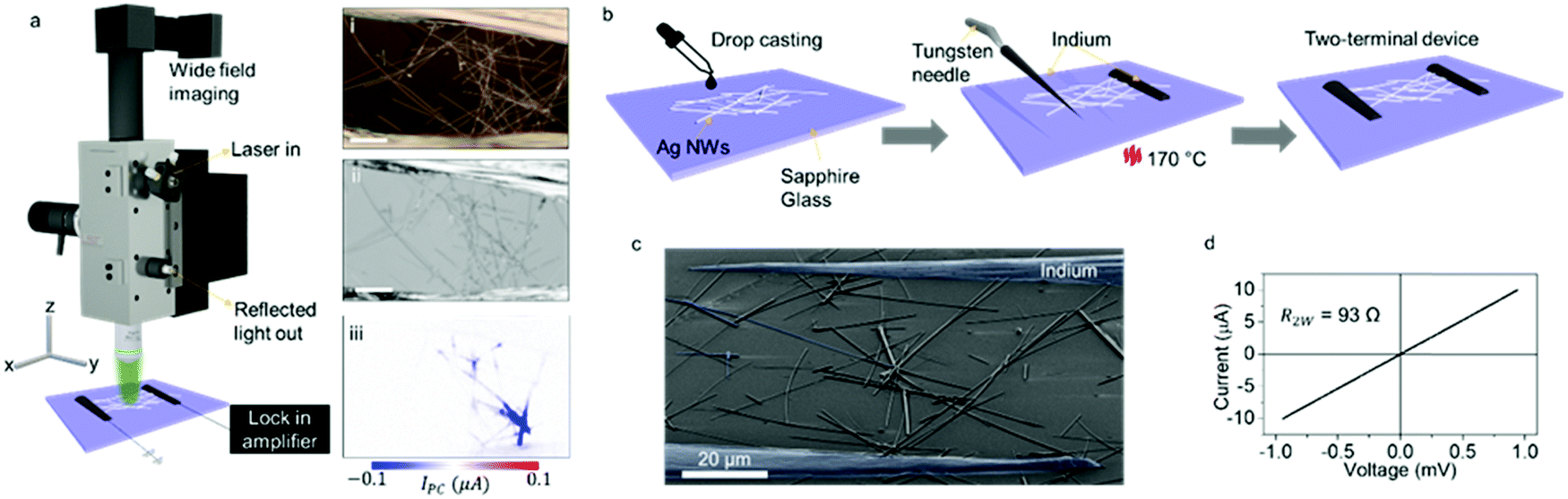 | ||
| Fig. 1 (a) Schematic of our SPCM setup: The continuous-wave laser beam focused on a diffraction-limited spot raster-scans the device. (i) The wide field reflection image, (ii) reflected light intensity map and (iii) generated photocurrent map of a typical device given in the panels on the right. The scale bars are 20 μm. (b) The device fabrication steps depicted: Ag NWs in IPA solution are drop-cast on a sapphire or glass substrate. The substrate with Ag NWs is heated to 170 °C and indium needles are placed over the nanowire network using a micromanipulator. Upon cooling, the device is ready for two-terminal electrical and scanning photocurrent measurements. (c) False-color SEM image of a typical device: Indium needles are shaded with blue. (d) Current vs. voltage graph showing the 2-wire resistance, R2W, of a typical device. | ||
First, we measured the photoresponse of the Ag NW network devices. Polyol process-synthesized Ag NWs in isopropyl alcohol (IPA) solution (Sigma Aldrich, 0.5 wt%) were used. The Ag NWs were characterized using X-ray diffraction (XRD), Raman spectroscopy, and X-ray photoelectron spectroscopy (XPS). Raman spectra collected from the nanowires reveal that polyvinylpyrrolidone (PVP) molecules from the synthesis cover the Ag NW surface (Fig. S2a, ESI†).24 PVP plays a part in the formation of the nanowires and protects the Ag NWs from the ambient environment.24 The XRD pattern (Fig. S2b, ESI†) matches with the face-centered-cubic Ag (ref. Card 98-005-3759) and finally XPS shows the metallic nature of the Ag nanowires (Fig. S2c, ESI†) (details are in the ESI†).
To fabricate the network devices, a 0.02 wt% Ag NW suspension was drop-cast onto a sapphire substrate (Fig. 1b). In the case of the fabrication of single nanowire devices, the suspension was diluted four times. Once the IPA evaporated, indium needles were placed as the electrical contacts. To place the indium needles on the Ag NW network, the substrate was heated to above 160 °C for several minutes (Fig. 1b). Once the indium needle contacted the hot substrate, it melted and formed the electrical connection with the Ag NW network. The high-temperature processing also significantly reduces the contact resistance as compared to the gold electrode devices before annealing.25 Despite the heating step, some devices exhibited large resistances on the order of MΩs. After biasing the devices, the resistances of most devices are reduced to a few tens of Ωs. Fig. 1c displays the false-colored SEM micrograph of a typical device and Fig. 1d shows its IV curve with the two-wire resistance of R2W = 93 Ω. Our Ag NW networks remained stable for an extended duration of up to 2 months after the fabrication.
SPCM maps taken on a Ag NW network device (Device #1) under 0, 100, and −100 mV are depicted in Fig. 2a–c, respectively (at an excitation wavelength λ = 532 nm and with laser power, P = 100 μW). The sign of the photocurrent (IPC) indicates the direction of the photo-induced current with respect to the lock-in amplifier. When the signal was into (out of) the lock-in amplifier, we registered a positive (negative) photocurrent. The reflection map corresponding to the SPCM maps is shown in Fig. 2d. 0 mV measurement shows that there is a weak photocurrent generation at certain parts of the network. We speculate that this is because of the plasmon-assisted heating of the Ag NW junctions, which leads to the Seebeck effect. A more detailed analysis is provided in the following paragraphs.
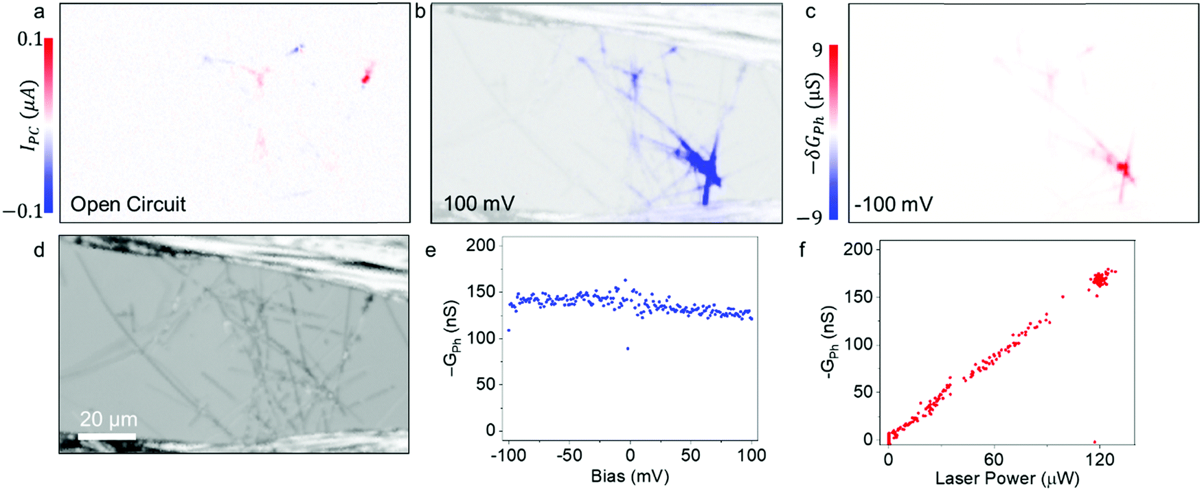 | ||
| Fig. 2 SPCM maps of a network device under (a) open-circuit (0 mV), and (b) 100 mV (overlaid over the reflection map for better positioning of the photoresponse locations). The scale is saturated to make all the features apparent. The maximum −IPC is 0.9 μA. It is noteworthy that there is a significant photoconductance change over the indium contacts and nanowires throughout the entire network. (c) −δGPh map plotted under −100 mV bias. (d) Reflection map showing the details of the network between the indium contacts. (a–d) have the same scale bar. (e) Negative photoconductance vs. applied bias measurement taken from a different network device showing a very small variation in the photoconductance across different biases. (f) Negative photoconductance increases linearly with the increasing laser power. The gap in the data points between 90 μW and 120 μW is due to the gap in the variable neutral density filter. | ||
When a bias was applied across the sample, a negative photoconductance (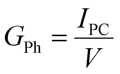 , where V is the applied bias) was observed along the NWs and in the vicinity of and at the NW–NW and NW–contact junctions. The local extrema of the photocurrent reside at the NW–NW junctions. Intriguingly, there is a considerable response from the indium contacts. The negative photoconductance over the indium contacts increases towards the nanowire junctions. It is unplausible for optical absorption mechanisms to increase the temperature increase in the thick (∼1 μm) indium contacts and result in a measurable photo-bolometric response from the indium needles. For similar reasons, without an enhanced heating mechanism the Seebeck effect from the indium–Ag NW junction is unexpected. Moreover, though Ag NWs exhibit a high temperature coefficient of resistance of ∼2 K−1 above 50 K,26 it is not possible for the laser powers employed in our experiments to lead to a measurable photo-bolometric response without a mechanism leading to local hot spot creation.
To explain the origins of the photoresponse observed in Ag NW networks, we conducted a series of controlled experiments. First, it is worth noting that the photoconductance is the same for different biases at points where there is no open circuit photoresponse, as shown in Fig. 2e. This photoconductance corresponds to an overall increase in the resistance of the network, 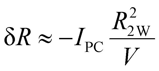 . For Device #1, δR = 0.052 Ω. This value is consistent with the finite element method simulation results (Fig. S3a and b, ESI†). The bolometric response is simulated with a point heat source located at the NW–NW junction. The local temperature rise of 5 K may result in a bolometric response of 50 mΩ, which is a plausible temperature rise for the laser powers employed in our experiments. We also measured −GPhvs. the incident laser power, given in Fig. 2f. The linear relation hints at a photo-thermal origin for the photoresponse.17,19,27,28
Next, we fabricated single nanowire devices and measured their photoresponse for a better understanding of the photoconductance in the network devices. We fabricated devices with two different contact configurations. In the first device configuration, the nanowires were placed over pre-patterned gold electrodes (Fig. 3a). Fig. 3b shows the reflection map (Fig. 3b-I) and the corresponding −GPh (Fig. 3b-II). There is a small open-circuit photocurrent (I0PC) over the contact regions marked in Fig. 3b-II. Fig. 3c-I displays the bias-dependence of −IPC in which −IPC linearly increases with the bias. −GPh exhibits a logarithmic growth (Fig. 3c-II). When the open-circuit response is subtracted from the rest of the photocurrent values, the photoconductance,  remains constant for the different biases. This is similar to what we observe in the network devices.
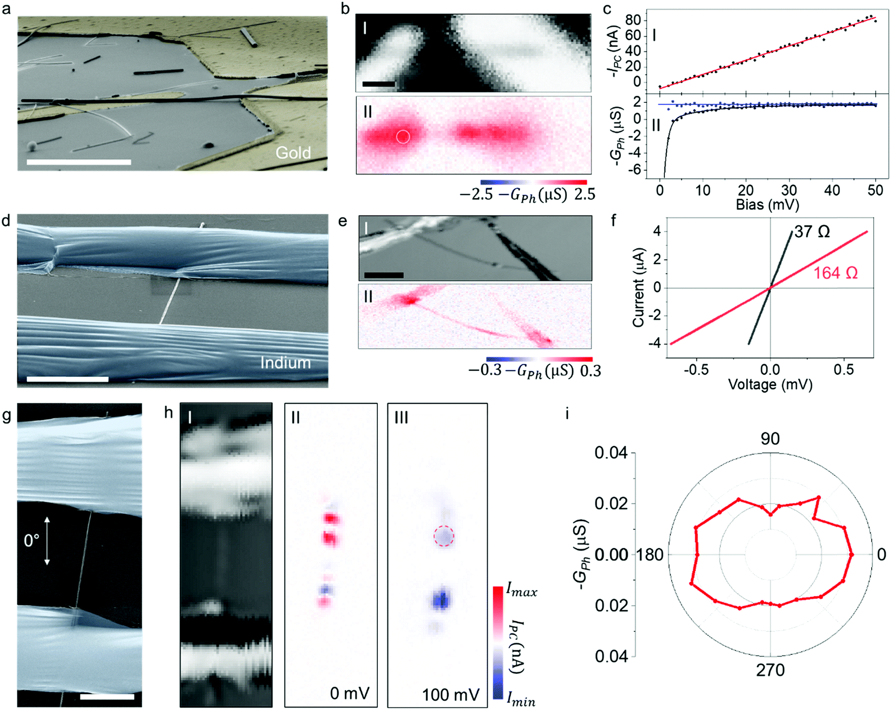 | ||
Fig. 3 (a). False colored SEM image of a Ag NW on pre-patterned gold electrodes. Scale bar is 5 μm. (b) Reflection map (I) and the corresponding −GPh map under 20 mV bias (II) showing the photoconductance over the device. It is noteworthy that there is a significant conductance modulation over the gold electrodes. A 532 nm laser source was used at 65 μW power. The yellow circle indicates the position where −IPCvs. bias measurements were taken from. The scale bar is 5 μm. (c) −IPCvs. bias (I) graph showing a linearly increasing −IPC with the bias (black dots). The red line is the linear fit to the data. Zero bias response is ∼6 nA. Lower panel (II) shows −GPh (black dots) and  (blue dots) vs. bias. Solid lines are fits to the data. (d) False colored SEM image of an indium contacted Ag NW. Note the grating-like structures over the indium, which naturally occur due to thermal contraction upon cooling. Scale bar is 5 μm. (e) Reflection map (I) and the corresponding −GPh map under 100 mV bias (II) showing the conductance modulation over the indium contacts. Notice that the modulation intensifies near the indium-NW junction. Also, the visible defect in the reflection map results in enhanced plasmonic response, which is clear in the photoconductance map. Data were collected with a 532 nm laser at 96 μW. Scale bar is 10 μm. (f) Current vs. voltage graphs of the same devices, before (red dots) and after (black dots) reduction of the photoconductance. (g) False colored SEM image of a device with the incident polarization angle marked. (h) (I) Reflection map, (II) open-circuit response, and (III) 100 mV response maps are shown. Imax = 0.25 nA for (II), 25 nA for (III) and Imin = −0.25 nA for (II) and −25 nA for (III). (i) The polar chart shows the incident polarization angle vs. −GPh at 100 mV bias. The data were collected from the individual maps taken around the red dashed circle in h (III). (blue dots) vs. bias. Solid lines are fits to the data. (d) False colored SEM image of an indium contacted Ag NW. Note the grating-like structures over the indium, which naturally occur due to thermal contraction upon cooling. Scale bar is 5 μm. (e) Reflection map (I) and the corresponding −GPh map under 100 mV bias (II) showing the conductance modulation over the indium contacts. Notice that the modulation intensifies near the indium-NW junction. Also, the visible defect in the reflection map results in enhanced plasmonic response, which is clear in the photoconductance map. Data were collected with a 532 nm laser at 96 μW. Scale bar is 10 μm. (f) Current vs. voltage graphs of the same devices, before (red dots) and after (black dots) reduction of the photoconductance. (g) False colored SEM image of a device with the incident polarization angle marked. (h) (I) Reflection map, (II) open-circuit response, and (III) 100 mV response maps are shown. Imax = 0.25 nA for (II), 25 nA for (III) and Imin = −0.25 nA for (II) and −25 nA for (III). (i) The polar chart shows the incident polarization angle vs. −GPh at 100 mV bias. The data were collected from the individual maps taken around the red dashed circle in h (III). | ||
In the second device configuration, indium needles were placed over a single nanowire (as depicted in Fig. 1b). Fig. 3d presents a false-color SEM image of a device. Fig. 3e shows the reflection map (Fig. 3e-I) and the corresponding photoconductance map (Fig. 3e-II) of the indium contacted single nanowire device (SEM images of the device are provided in the ESI,† Fig. S4). In both device configurations strong negative photoconductance at the metal contact-nanowire junction region, mostly over the electrodes is observed. This hints that the photoconductance modulation comes from the plasmonic heating effects at the naturally occurring gaps between the nanowires and the contact metals as other photoresponse mechanisms are unplausible.
Now we would like to hypothesize and elucidate the mechanisms leading to the photocurrent generation over the electrode region near the electrode-NW junction. To explain the photocurrent generation mechanism over the metal electrodes, we hypothesize that the SPPs created at the rough contact metal surfaces reach the junction between the Ag NW and the contact metal and generate localized hot spots. As briefly discussed earlier, Ag NWs exhibit a high temperature coefficient of resistance and the temperature rise at the junctions can result in a bolometric response. Fig. S5 (ESI†) shows the bolometric response of a network device under homogenous heating. Despite the relatively small laser powers employed in our experiments, the junctions can be heated up by a few to a few tens of Kelvin8,10,29 and this may lead to a measurable change in the overall photoconductance of the nanowire. For the plasmon-enhanced heating, SPP creation is needed. The creation of SPP requires matching the wave vector of the incident photon to that of the SPP modes.30 This can be achieved by frustrating the incident electromagnetic wave through surface roughness or with grating structures on the metal surface.31,32 Moreover, SPP creation is highly dependent on the orientation of the incident light polarization.
To test the hypothesis stated in the previous paragraph, we conducted a series of experiments. First, we would like to note that the contact resistance plays a detrimental role in determining the photoresponse of metallic materials.17 Due to the PVP coverage of Ag NWs, making electrical connection with small contact resistance requires welding of NWs to each other and to the contacts.12 To begin with, we measured the 2-wire resistance of a single nanowire device as 164 Ω before the SPCM experiments. After 81 SPCM mappings under various testing conditions, the photoresponse disappeared and the 2-wire resistance dropped down to 37 Ω (Fig. 3f). The significantly improved resistance value shows that the contact resistance of the device is reduced by fusing the contact metal to the Ag NW.33 It can be speculated that the contact resistance improvement is due to the SPP-assisted heating generated at the contact region or due to Joule heating as the device is under bias during SPCM measurements.34 Another possibility that may lead to the decrease in the resistance is the interface reconstruction due to electromigration in Ag NWs.35 Regardless of the possible mechanisms, the naturally occurring gaps between the NW and the contact close and the SPP-assisted bolometric effect emerging at the contacts disappears.
Another observation that supports the SPP-assisted heating at the NW-contact junction hypothesis is that the photoresponse is generated mostly over the gold surface and the indium contacts in single NW devices and in the vicinity of the NW-metal junction. The responses from the metal junctions exhibit the same photoconductance sign and their relative intensities can be dramatically different from each other. This indicates that the phenomena that lead to the optical response are independent of the contact configuration of the devices. Among the known photoresponse mechanisms, only the sign of the signal generated by the bolometric effect is not affected by the contact configuration. Also, it is worth noting that grating-like structures that naturally form on the surface of the indium needles, as shown in the SEM image in Fig. 3d, can provide an efficient path for SPP creation. The period of the features is mostly uniform over the region of interest, and for the device shown in Fig. 3d, the grating period is ∼500 nm.
To further demonstrate the role of the SPP-enhanced bolometric effect at the nanowire-metal junctions, we investigated the polarization-dependence of the observed photoresponse. We performed these experiments by rotating the polarization angle of the incident beam with respect to the Ag NW. For the polarization-dependent experiments, we used a 632.8 nm HeNe laser source. Details of the polarization-dependent measurements are provided in the ESI.†Fig. 3g shows the SEM image of a nanowire we tested for the polarization-dependent photoresponse. SPCM reflection map and the photocurrent maps at 0 and 100 mV biases obtained with 532 nm excitation are given in Fig. 3h. Under zero bias, IPC alternates between negative and positive responses with a period of 2.4 μm. When 100 mV is applied, IPC becomes −25 nA with no positive signal remaining. Fig. 3i shows the polar plot of the incident polarization vs. −GPh taken from the red dashed circle in Fig. 3h-III. The strong incident polarization angle-dependence of the photoresponse suggests the plasmonic nature of the observed signal.
Now, we focus on the open circuit-response. Open-circuit response was observed in both the network and single nanowire devices. As the network devices consist of many NW–NW junctions we focused our attention on simpler single NW devices as seen in Fig. 3h-II. We consider this response to be due to the Seebeck effect because of the SPP-assisted heating of the Ag-In junctions. The signal along the crystal is likely to be due to the undulations of the silver nanowires after biased measurements. A further explanation of the alternating photoresponse is provided in the ESI.† The Seebeck coefficient difference between Ag and In is ΔSAg−In ≈ 0.3 μV K−1.36,37 The device we measured in Fig. 3g has 6 Ω resistance. This means the emf generated by the Seebeck effect is ∼1 nV. Based on ΔSAg−In we can estimate that the junction temperature is raised by ∼5 mK for 100 μW laser power in this sample.
The plasmonic coupling to the incident laser beam can be enhanced by decorating the nanowires with nanoparticles.38–40 This will create more SPPs and plasmonic heating at the nanoparticle-NW gap will be distributed across the length of a nanowire, which should increase the bolometric response observed as compared to that of the bare Ag NW devices, where the signal only emerges from the contact-NW junction. To test this idea, we fabricated an Ag NW network device on a glass substrate and decorated it with Ag nanoparticles (NPs) of 20 ± 5 nm in diameter (see ESI† for details).41Fig. 4a shows the saturated SPCM map (with indium contacts outlined) to reveal fainter features that lie outside of the contacts and over the indium. Fig. 4b shows the unsaturated map of the section outlined in Fig. 4a. The device reported here exhibits 130 mA W−1 responsivity, determined by the ratio of the generated photocurrent over the incident laser power. This is more than an order of magnitude larger than the response from the network device reported in Fig. 2, where responsivity is measured as 9 mA W−1.
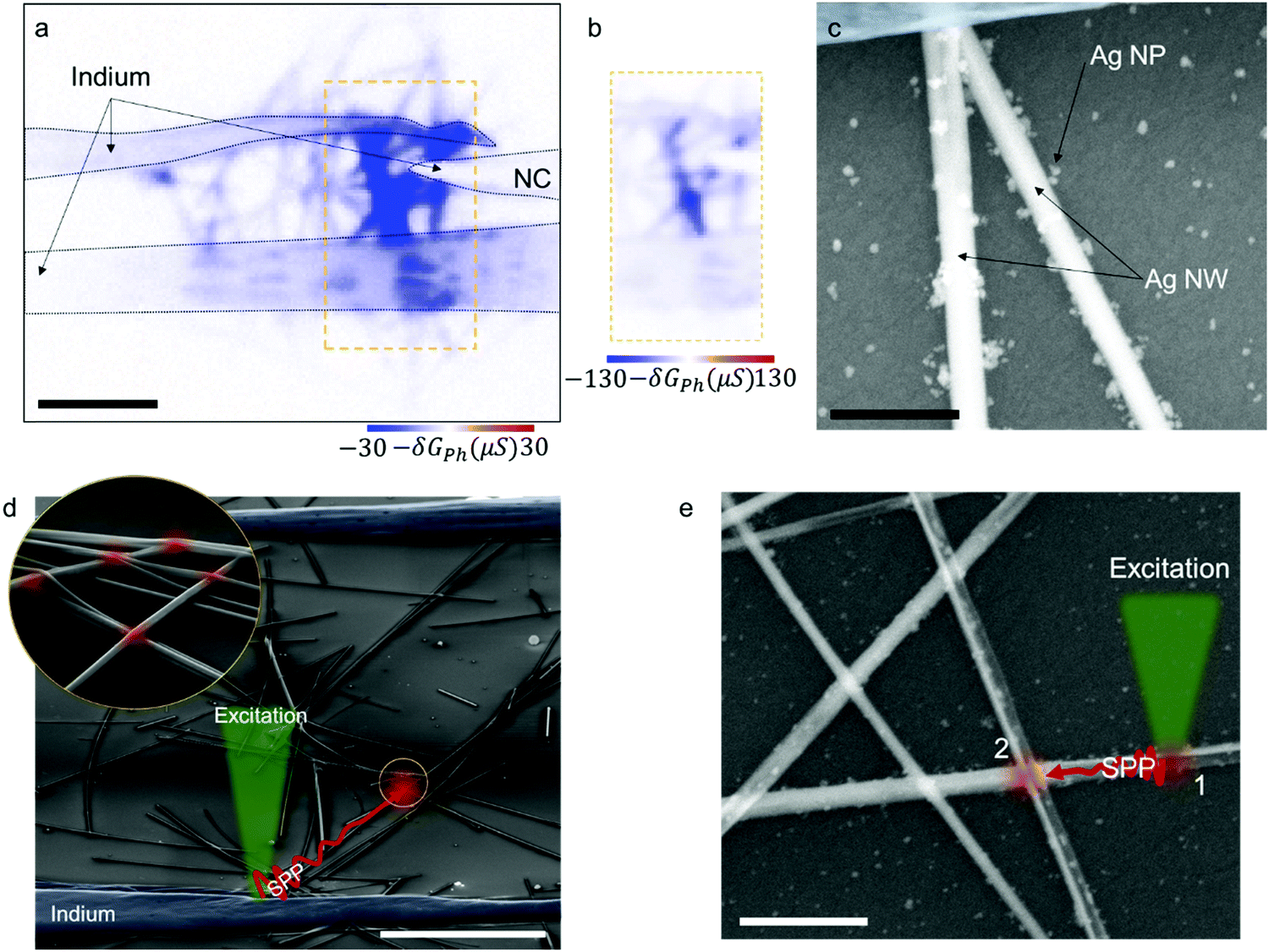 | ||
| Fig. 4 (a). Photoconductance map of an Ag NP-decorated network device under a −100 mV bias. Outlines of the indium contacts are marked with black dashed lines. The needle on the right side marked with NC is an indium needle that was not connected to the device electrically. The map scale is saturated to reveal the photoconductance change over the Ag NWs outside of the device and over the indium needles. Maps were taken with a 532 nm laser at 93 μW. The scale bar is 10 μm. (b) Unsaturated −δGPh map of the area marked with the yellow dashed rectangle in (a and c) Close-up SEM micrograph of Ag NWs decorated with Ag NPs. Indium contact is false-colored with blue. The scale bar is 500 nm. (d) SPP-assisted bolometric response depicted in a false-colored SEM image. The excitation creates SPPs at the contacts or regions where the light coupling to the metal structure is possible. The SPPs travel to the NW–NW junctions and the local field enhancement creates hot spots. The scale bar is 20 μm. (e) A similar mechanism is depicted in the SEM image of Ag NP-decorated Ag NWs. The light coupling is possible near the nanowires thanks to the Ag NPs, which create two hot spots, marked with 1 and 2 on the SEM image. The scale bar is 1 μm. | ||
Here, as we predicted, all the nanowires connected to the indium exhibit a photoresponse. This is due to the enhanced light coupling to the metallic structures thanks to the Ag NPs in the vicinity of the Ag NWs and shows that the photoresponse is not a local response, rather SPPs traveling to the relevant junctions cause the photoresponse over the nanowires as explained in undecorated devices. Also, the response is spread all over the Ag NWs and the response is significantly enhanced thanks to the heating that takes place due to the field enhancement at the NW–NP junction. Fig. 4c shows a close-up SEM image of the Ag NP-decorated network device in which Ag NPs are clearly visible in the vicinity of the NWs. The other interesting observation consistent with the undecorated devices is the enhanced photoresponse from the grating-like features over the indium contacts. Fig. 4d depicts the creation of SPPs over the metal contacts and creation of local hot spots at the NW–NW junctions, which result in the bolometric response observed in the device. Similarly, Fig. 4e depicts the coupling of the incident light to the SPPs to create hot spots both locally and at the NW–NW junction at a distance.
In summary, here we reported the photoresponse from single Ag NWs and their networks. Our findings reveal that the plasmonic effects result in enhanced photo-bolometric response and the Seebeck response in the single Ag NWs and their networks. Moreover, decorating the Ag NWs with Ag nanoparticles results in a modified photoresponse. These findings may enable a facile way to fabricate and more importantly measure all-metallic photo-sensitive optoelectronic devices and sensors. As such, attaching capture antibodies over the Ag NW network may result in a detectable change in the photocurrent generation in the presence or in the absence of the target molecules.42
Author contributions
T. S. K. designed and conducted the experiments. M. R. and M. U. performed the experiments with the help of T. S. K. F. S. and H. V. D. provided the nanoparticles. All the authors discussed the results and contributed to the writing of the manuscript.Conflicts of interest
There are no conflicts to declare.Acknowledgements
T. S. K. acknowledges funding from the Scientific and Technological Research Council of Turkey (TUBITAK) under grant number 118F061. We would like to thank Prof. Hüsnü Emrah Ünalan for providing useful feedback on the manuscript and the Ag NWs for the preliminary experiments. We also would like to thank Prof. Fatih İnci for his useful comments on the manuscript.References
- W. Li, H. Zhang, S. Shi, J. Xu, X. Qin, Q. He, K. Yang, W. Dai, G. Liu, Q. Zhou, H. Yu, S. R. P. Silva and M. Fahlman, J. Mater. Chem. C, 2020, 8, 4636–4674 RSC.
- H. Ditlbacher, A. Hohenau, D. Wagner, U. Kreibig, M. Rogers, F. Hofer, F. R. Aussenegg and J. R. Krenn, Phys. Rev. Lett., 2005, 95, 257403 CrossRef PubMed.
- J. A. Schuller, E. S. Barnard, W. Cai, Y. C. Jun, J. S. White and M. L. Brongersma, Nat. Mater., 2010, 9, 193–204 CrossRef CAS PubMed.
- M. Rycenga, C. M. Cobley, J. Zeng, W. Li, C. H. Moran, Q. Zhang, D. Qin and Y. Xia, Chem. Rev., 2011, 111, 3669–3712 CrossRef CAS PubMed.
- H. Wei, D. Pan, S. Zhang, Z. Li, Q. Li, N. Liu, W. Wang and H. Xu, Chem. Rev., 2018, 118, 2882–2926 CrossRef CAS PubMed.
- N. J. Halas, S. Lal, W. S. Chang, S. Link and P. Nordlander, Chem. Rev., 2011, 111, 3913–3961 CrossRef CAS PubMed.
- J. B. Herzog, M. W. Knight and D. Natelson, Nano Lett., 2014, 14, 499–503 CrossRef CAS PubMed.
- J. H. Park, G. T. Hwang, S. Kim, J. Seo, H. J. Park, K. Yu, T. S. Kim and K. J. Lee, Adv. Mater., 2017, 29, 1603473 CrossRef PubMed.
- G. Qiu, Z. Gai, Y. Tao, J. Schmitt, G. A. Kullak-Ublick and J. Wang, ACS Nano, 2020, 14, 5268–5277 CrossRef CAS PubMed.
- E. C. Garnett, W. Cai, J. J. Cha, F. Mahmood, S. T. Connor, M. Greyson Christoforo, Y. Cui, M. D. McGehee and M. L. Brongersma, Nat. Mater., 2012, 11, 241–249 CrossRef CAS PubMed.
- W. H. Chung, Y. R. Jang, Y. T. Hwang, S. H. Kim and H. S. Kim, Nanoscale, 2020, 12, 17725–17737 RSC.
- Y. Ding, Y. Cui, X. Liu, G. Liu and F. Shan, Appl. Mater. Today, 2020, 20, 100634 CrossRef.
- G. Buchs, S. Bagiante and G. A. Steele, Nat. Commun., 2014, 5, 1–6 Search PubMed.
- J. C. W. Song, M. S. Rudner, C. M. Marcus and L. S. Levitov, Nano Lett., 2011, 11, 4688–4692 CrossRef CAS PubMed.
- X. N. Xie, Y. Xie, X. Gao, C. H. Sow and A. T. S. Wee, Adv. Mater., 2009, 21, 3016–3021 CrossRef CAS.
- N. M. Gabor, J. C. W. Song, Q. Ma, N. L. Nair, T. Taychatanapat, K. Watanabe, T. Taniguchi, L. S. Levitov and P. Jarillo-Herrero, Science, 2011, 334, 648–652 CrossRef CAS PubMed.
- N. Mehmood, H. R. Rasouli, O. Çakıroğlu and T. S. Kasırga, Phys. Rev. B, 2018, 97, 195412 CrossRef CAS.
- A. O. Govorov, H. Zhang, H. V. Demir and Y. K. Gun’Ko, Nano Today, 2014, 9, 85–101 CrossRef CAS.
- T. S. Kasirga, D. Sun, J. H. Park, J. M. Coy, Z. Fei, X. Xu and D. H. Cobden, Nat. Nanotechnol., 2012, 7, 723–727 CrossRef CAS PubMed.
- M. Barkelid and V. Zwiller, Nat. Photonics, 2014, 8, 47–51 CrossRef CAS.
- M. A. Mangold, C. Weiss, M. Calame and A. W. Holleitner, Appl. Phys. Lett., 2009, 94, 3–5 CrossRef.
- H. Zhu, H. Xie, Y. Yang, K. Wang, F. Zhao, W. Ye and W. Ni, Nano Lett., 2020, 20, 2423–2431 CrossRef CAS PubMed.
- R. E. Vest and S. Grantham, Appl. Opt., 2003, 42, 5054 CrossRef CAS PubMed.
- H. Mao, J. Feng, X. Ma, C. Wu and X. Zhao, J. Nanopart. Res., 2012, 14, 887 CrossRef.
- D. P. Langley, M. Lagrange, G. Giusti, C. Jiménez, Y. Bréchet, N. D. Nguyen and D. Bellet, Nanoscale, 2014, 6, 13535–13543 RSC.
- Z. Cheng, L. Liu, S. Xu, M. Lu and X. Wang, Sci. Rep., 2015, 5, 10718 CrossRef CAS PubMed.
- O. Çakıroğlu, N. Mehmood, M. M. Çiçek, A. Aikebaier, H. R. Rasouli, E. Durgun and T. S. Kasırga, 2D Mater., 2020, 7, 035003 CrossRef.
- T. S. Kasirga, Thermal Conductivity Measurements in Atomically Thin Materials and Devices, Springer Singapore, Singapore, 2020 Search PubMed.
- C. I. Evans, P. Zolotavin, A. Alabastri, J. Yang, P. Nordlander and D. Natelson, Nano Lett., 2017, 17, 5646–5652 CrossRef CAS PubMed.
- E. Kretschmann and H. Raether, Z. Naturforsch., A: Phys. Sci., 1968, 23, 2135–2136 CAS.
- Y.-Y. Teng and E. A. Stern, Phys. Rev. Lett., 1967, 19, 511–514 CrossRef.
- N. E. Glass, A. A. Maradudin and V. Celli, Phys. Rev. B: Condens. Matter Mater. Phys., 1982, 26, 5357–5365 CrossRef CAS.
- Y. Zhao, M. L. Fitzgerald, Y. Tao, Z. Pan, G. Sauti, D. Xu, Y. Q. Xu and D. Li, Nano Lett., 2020, 20, 7389–7396 CrossRef CAS PubMed.
- T. Bin Song, Y. Chen, C. H. Chung, Y. Yang, B. Bob, H. S. Duan, G. Li, K. N. Tu and Y. Huang, ACS Nano, 2014, 8, 2804–2811 CrossRef PubMed.
- B. Stahlmecke, F.-J. M. Zu Heringdorf, L. I. Chelaru, M. H. Hoegen, G. Dumpich and K. R. Roos, Appl. Phys. Lett., 2006, 88, 053122 CrossRef.
- M. Kockert, D. Kojda, R. Mitdank, A. Mogilatenko, Z. Wang, J. Ruhhammer, M. Kroener, P. Woias and S. F. Fischer, Sci. Rep., 2019, 9, 1–8 Search PubMed.
- Thermal Conductivity: Proceedings of the Seventh Conference Held at the National Bureau of Standards, D. R. Flynn and B. A. Peavy, ed., US Department of Commerce, National Bureau of Standards, Gaithersburg, Maryland, 1967 Search PubMed.
- M. Davies, A. Wochnik, F. Feil, C. Jung, C. Bräuchle, C. Scheu and J. Michaelis, ACS Nano, 2012, 6, 6049–6057 CrossRef CAS PubMed.
- Z. Fang, L. Fan, C. Lin, D. Zhang, A. J. Meixner and X. Zhu, Nano Lett., 2011, 11, 1676–1680 CrossRef CAS PubMed.
- T. Kim, S. Kang, J. Heo, S. Cho, J. W. Kim, A. Choe, B. Walker, R. Shanker, H. Ko and J. Y. Kim, Adv. Mater., 2018, 30, 1800659 CrossRef PubMed.
- M. Chen, Y. G. Feng, X. Wang, T. C. Li, J. Y. Zhang and D. J. Qian, Langmuir, 2007, 23, 5296–5304 CrossRef CAS PubMed.
- Z. Li, L. Leustean, F. Inci, M. Zheng, U. Demirci and S. Wang, Biotechnol. Adv., 2019, 37, 107440 CrossRef CAS PubMed.
Footnote |
| † Electronic supplementary information (ESI) available. See DOI: 10.1039/d1nh00629k |
| This journal is © The Royal Society of Chemistry 2022 |