
 Open Access Article
 This Open Access Article is licensed under a Creative Commons Attribution-Non Commercial 3.0 Unported Licence
Facile and stable fabrication of wafer-scale, ultra-black c-silicon with 3D nano/micro hybrid structures for solar cells
Xiaomeng
Zhang
ab,
Yu
Liu
a,
Chuhao
Yao
ab,
Jiebin
Niu
a,
Hailiang
Li
 *a and
Changqing
Xie
*a
*a and
Changqing
Xie
*a
aKey Laboratory of Microelectronic Devices & Integrated Technology, Institute of Microelectronics of Chinese Academy of Sciences, Beijing 100029, People's Republic of China. E-mail: lihailiang@ime.ac.cn; xiechangqing@ime.ac.cn; Tel: +86-010-82995581.
bUniversity of Chinese Academy of Sciences, Beijing 100049, People's Republic of China
First published on 3rd November 2022
Abstract
Three-dimensional (3D) silicon (Si) nanostructures have attracted much attention in solar cells due to their excellent broadband and omnidirectional light-harvesting properties. However, the development of 3D Si nanostructures is still plagued by the trade-off between structural complexity and fabrication difficulty. Herein, we proposed a facile and stable approach toward the fabrication of wafer-scale, ultra-black crystalline silicon (c-Si) with nano/micro hybrid structures. The distinguishing advantage of this approach is that it allows the formation of 3D Si nano/micro hybrid structures in a single-round process, avoiding the need for multiple iterations of lithography, coating, and etching required in conventional processes. The nano/micro hybrid structure arrays we fabricated show a low reflectance of <1% in the 600–1000 nm wavelength range and absorb 98.82% of incident light in the visible and near-infrared regions from 400 to 1100 nm under AM 1.5 G illumination. Solar cells made from nano/micro hybrid 3D structure arrays have an efficiency improvement of about 11.4% compared to those made from mono-micropillar arrays, and they have potential applications in high-performance photovoltaic devices.
Introduction
As one of the most important materials, silicon (Si) has been widely used in the field of optical and optoelectronic devices.1–4 The absorption of light by Si occurs below 1100 nm, corresponding to the energy band gap of single-crystal Si. However, the light collection efficiency at the Si surface is not high enough due to the large refractive index (RI) of Si resulting in a relatively high reflectivity at the air/Si interface, which greatly limits its application in photovoltaic cells.5 Although various light management strategies (e.g., anti-reflective coatings and surface plasmon resonance) have been implemented, only a limited increase in light absorption can be achieved using one of the above strategies.6 In addition, factors such as small working angles and mismatched thermal properties of different materials limit the application of these approaches in certain devices, making it far from being sufficient for practical needs.7Black Si based on mono-nano or microstructures, such as nanowire,8 micropillar,9 and nanocone10 arrays bypasses these limitations and have attracted much attention for anti-reflection devices because of their excellent broadband and omnidirectional light harvesting properties.11 The prepared black Si can achieve high light absorption in the visible to near-infrared (NIR) range.12 Kumar et al. fabricated black Si based on Si nanowire (SiNW) arrays and applied them in solar cells.13 The maximum reflection of the black Si surface was approximately 4% between 300 and 1000 nm. However, SiNW arrays have a high aspect ratio, indicating a very high surface-to-volume ratio that increases the probability of surface recombination and difficulties in producing the top electrodes. Surface recombination leads to a decrease in the short-circuit current density (Jsc) and open-circuit voltage (Voc) of the solar cells. Thus, the fabrication of highly efficient SiNW array solar cells is difficult. On the other hand, black Si based on micropillar arrays permit the formation of a stable emitter, enabling effective carrier collection using general grid-type metal electrodes without transparent conducting electrodes.14 However, the light absorption of micropillar arrays is poor compared to that of SiNW arrays because of their higher surface reflection.15 Therefore, a nano/micro hybrid structure is necessary for the development of efficient radial junction solar cells.
A nano/micro hybrid structure can be explored in various fields such as microelectronics,16 optoelectronics,17 photonics,18 biology,19 and sensors,20–22 especially in photovoltaics.23,24 It combines the advantages of microstructures and nanostructures, which not only possess strong light absorption due to the top SiNW arrays but also efficient carrier collection induced by the radial p–n junction of the micropillar arrays.9 To achieve black Si based on nano/micro hybrid structures for solar cells, photolithography, electron beam lithography (EBL), and reactive ion etching (RIE) approaches were widely exploited.25,26 Xu et al. used potassium hydroxide (KOH) wet etching followed by RIE approaches achieving nano-texture on a micron-pyramid surface.27 However, not only do these processes rely on complex repetitive lithography and etching, but RIE can also significantly affect the roughness of the structure surface and even cause surface damage,28 which can reduce the lifetime of the minority carriers and decrease Voc.29 In recent years, metal-assisted chemical etching (MacEtch) has emerged as a promising low-cost alternative method capable of fabricating 3D black Si based on nano- and micro-structures of a variety of shapes and applications.30–32 To achieve nano/micro hybrid structures, MacEtch is performed through photolithography and ion beam etching to form micropillar arrays and SiNW arrays, respectively, to produce radial junction solar cells.8,33,34
In this work, we proposed a facile and stable approach toward the preparation of wafer-scale ultra-black crystalline Si (c-Si) with nano/micro hybrid structures. The key strategy of this approach is to use the physical bombardment of ion beam etching to simultaneously form the nano- and micro-catalytic structures required for subsequent MacEtch in a single step, which we refer to here as the “one-step MacEtch” approach, thus avoiding the need for multiple iterations of lithography, coating, and etching required in conventional processes. The nano/micro hybrid structure arrays combined the advantages of nanowires and micropillars in photovoltaic cell applications and showed a low reflectance of <1% in the 600–1000 nm wavelength range and absorbed 98.82% of the incident light in the visible and near-infrared regions from 400 to 1100 nm under AM 1.5 G illumination. This efficiency improvement is about 11.4% compared to that of conventional micropillar array solar cells, which hold potential applications in high-performance photovoltaic devices.
Results and discussion
Basic concept
In a typical MacEtch approach, a metal-patterned Si substrate is immersed in a solution of HF, H2O2, and deionized water. The metal acts as a catalyst for the re duction of H2O2, and with it, holes are injected deep into the valence band of the Si substrate. The concentration of holes becomes higher in the Si region beneath the metal catalyst.35 There, Si is readily oxidized and dissolved in HF, forming silicon fluoride compounds. As the reaction continues, the remaining Si that is far from the metal pattern and not oxidized forms nano- or micro-structures. By modulating the etching time and the ratio of the etching solution, different etching reaction kinetics can be obtained to yield different morphological features.35–37The basic concept of the “one-step MacEtch” fabrication strategy to obtain nano/micro hybrid structure arrays is schematically shown in Fig. 1b. In this “one-step MacEtch” process, starting from a single crystal Si substrate coated with a catalytic metal film and photoresist (i), we pattern the photoresist by using UV lithography in hard contact mode (ii). After that, the photoresist pattern is transferred to the metal film using ion beam etching (iii). It is important to note here that the ion beam etches away the metal not protected by the photoresist while physically bombarding some of the metal particles and implanting them on the surface of the Si. Finally, after removing the photoresist, MacEtch is performed in the solution of HF, H2O2, and deionized water to form nano/micro hybrid structure arrays (iv and v). The key to this fabrication approach is to use the physical bombardment of ion beam etching to simultaneously form the nano- and micro-catalytic structures required for subsequent MacEtch in a single step, thus avoiding the complex repetitive lithography and etching required by conventional processes38 (as shown in Fig. 1a) to achieve nano/micro hybrid structures. An optical image of the fabricated nano/micro hybrid structure arrays on a 4-inch Si wafer is shown in Fig. 1c. The optical image of the nano/micro hybrid structures on the c-Si wafer appears black, which indicates that there is hardly any reflection of light from its surface, and we can speculate that it has near-blackbody absorption properties. Fig. 1d–g shows the SEM images of the fabricated nano/micro hybrid structure arrays with a pitch of 20 μm, a gap of 2 μm, and a height of ∼180 μm. As shown in Fig. 1d and e, nanostructures were evenly formed only on the top (∼50 nm of thickness) of the high-aspect-ratio micropillars, thereby minimizing the impact of surface recombination occurring in the nanostructures and maximizing light absorption.
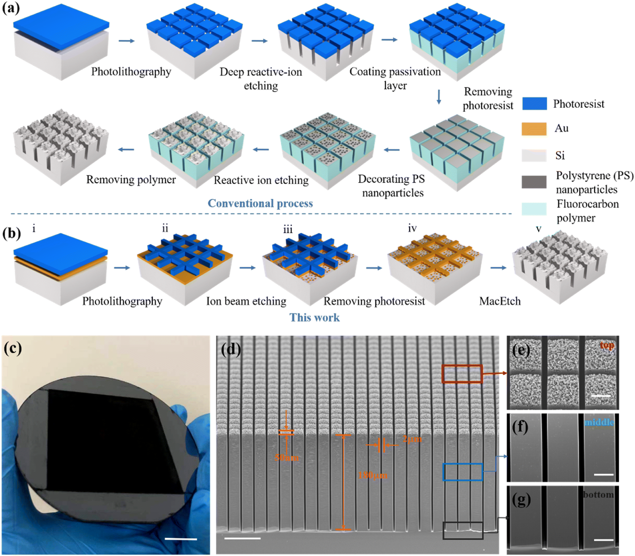 | ||
| Fig. 1 Comparison of the “one-step MacEtch” approach with the conventional etching process to fabricate nano/micro hybrid structures. (a) The conventional process, in which the steps of patterning, dry etching, and cleaning need to be repeated more than twice, is very complicated. (b) The “one-step MacEtch” approach, in which the patterning, etching, and cleaning steps are all completed in a single cycle, is both facile and cost-effective. (c) An optical image of the fabricated nano/micro hybrid structure arrays on a 4-inch Si wafer. The scale bar is 20 mm. (d) Tilted view SEM image of nano/micro hybrid structure arrays. The scale bar is 40 μm. SEM images of the top (e) middle (f) and bottom (g) regions of the nano/micro hybrid structures. The scale bars are 13 μm. | ||
Concept demonstration
As a proof of concept, Fig. 2 demonstrates the fabrication of nano- and micro structure arrays via the “one-step MacEtch” approach. The scanning electron microscopy (SEM) image (Fig. 2a) of catalytic gold (Au) structures patterned by ion beam etching was given, showing that they are well defined. The uniformity of the surface was further confirmed using energy-dispersive X-ray spectroscopy (EDS) in conjunction with SEM to scan the elemental mapping of the patterned surface before MacEtch, as shown in Fig. 2b and c. It can be seen that the Au particles are homogeneously distributed on the Si surface. The presence of the oxygen element may be attributed to the native oxide layer on the Si surface. The effects of the ion beam etching time on the morphology of the Si nanostructures were also investigated. Fig. 2d and e show the EDS maps of the Au particle distribution with different ion beam etching times and the corresponding SEM images of the Si structures after MacEtch, respectively. The etching time of the ion beam has a very strong influence on the surface morphology of the Si structure. The columns from left to right correspond to different etching times of 40, 60, 80, 100, and 120 seconds, respectively. As the etching time of the ion beam increases, the amount of unetched Au particles on top of the micropillar becomes scarcer and the surface texture of the nano/micro hybrid structure gradually tends to be flat. The interconnectedness of the micro-level catalytic structure forces it to sink harmoniously into the Si to achieve microstructures. With the decrease in the etching time, the etching of metal is insufficient and there will be more Au particle residue on the top of the micropillar region, so when the etching time is less than 40 s, the interconnectedness of the metal catalyst is disrupted by the traction of residual excess Au particles, forcing it to sink unharmoniously downward into the Si, which leads to non-uniform surface morphology over a large area. Therefore, to obtain a uniform, dense, and sharp nanostructure on the surface of the Si structure, an optimal etching time of 60 seconds was chosen. Since the micro-level catalytic structure is a mesh, which is interlocked as shown in Fig. 2a, it can etch down steadily around the micro-pillar tens of microns deep after entering the etchant. While the nanoscale catalysts, as can be seen in Fig. 2d, are isolated gold particles which are not subject to any constraint during the etching process, they can move randomly in all directions. Eventually the nanoscale catalytic particles at the top of the micropillars all move into the etching solution, at which point nanoscale etching stops, so the average depth of etching is only few tens of nanometers.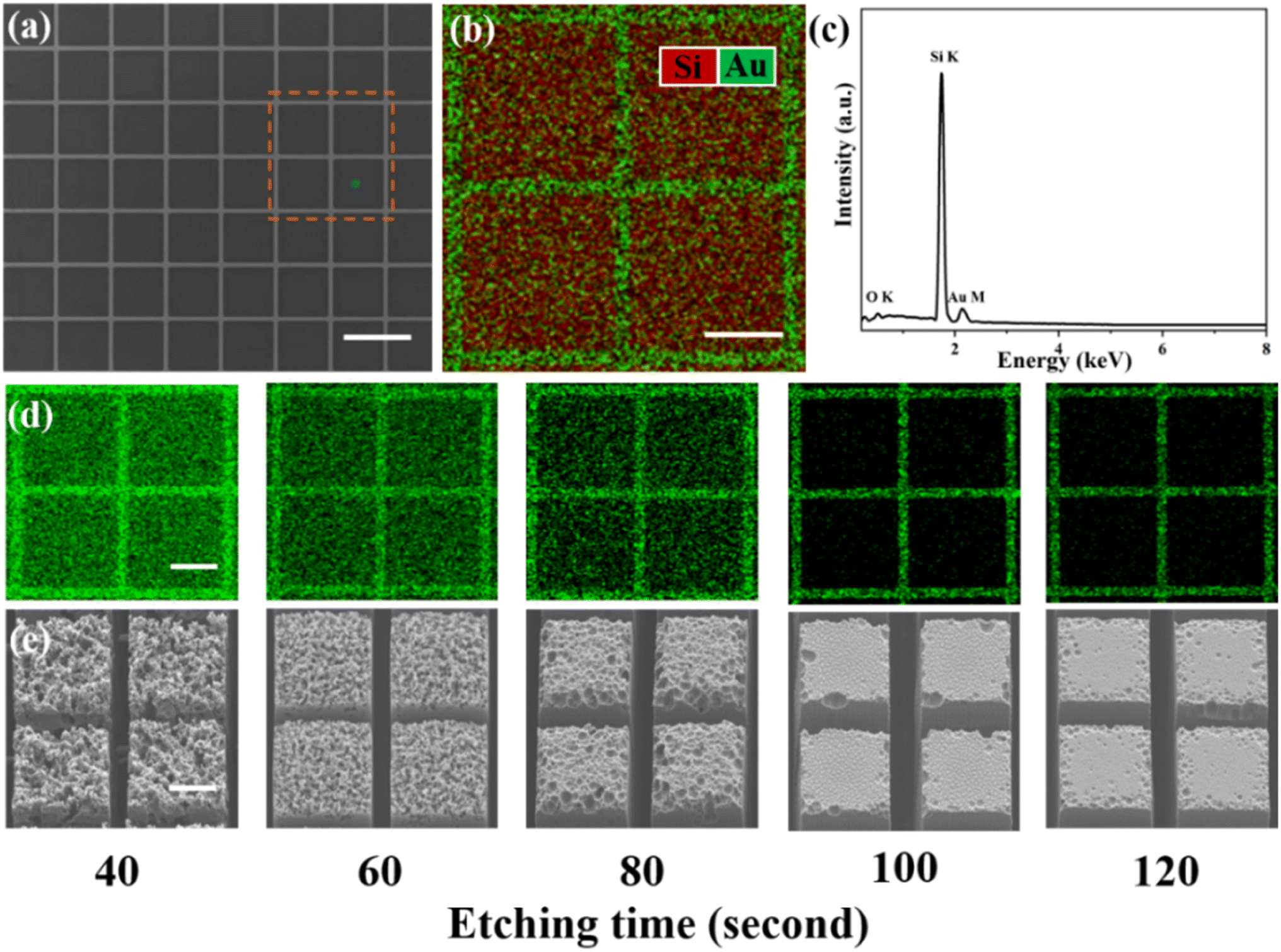 | ||
| Fig. 2 Experimental demonstration of the fabrication process flow for obtaining nano/micro hybrid structure arrays by using the “one-step MacEtch” approach. (a) SEM image of catalytic Au structures formed by ion beam etching. The scale bar is 20 μm. (b) and (c) EDS mapping measurement of the orange box in panel (a), displaying the element distribution after ion beam etching. The scale bar is 10 μm. (d) EDS mapping measurement of the nano/micro hybrid structures after ion beam etching versus etching time from 40 to 120 s. (e) Top-view SEM images of the nano/micro hybrid structures after MacEtch versus ion beam etching time from 40 to 120 s. The scale bars of (d) and (e) are 10 μm. | ||
Arbitrary geometries
To further demonstrate the facile and stable nature of this “one-step MacEtch” approach, arrays of nano/micro hybrid structures with different geometries were designed and fabricated, as shown in Fig. 3. At first, we designed robust hydrophobic surfaces on which three different shapes (circle, rectangle, and triangle) of a nano/micro hybrid structure array are obtained, as shown in Fig. 3a–d. Fig. 3a and b show circles arranged at different pitches. It is well known that these structures represent the most used hydrophobic surfaces because their patterned superhydrophobic properties and textured surfaces can be more hydrophobic than smooth surfaces. From the SEM images in Fig. 3d, it was observed that the sharp corners of the nano/micro hybrid structure (particularly triangular edges) were rounded due to the limitation of the present UV-photolithography process. To further confirm the versatility of this approach, nano/micro hybrid structures with multiscale geometry were fabricated simultaneously with this “one-step MacEtch” approach. Fig. 3f shows a series of circle-shaped structures with varied diameters from 2 μm to 6 μm fabricated by this method. In addition, this approach also enables obtaining complex structures. We designed and fabricated “pentagram” -shaped and “peanut”-shaped structures as shown in Fig. 3g and h, respectively. So, functional structures which are not feasible or extremely challenging to fabricate by any other methods can be readily fabricated by our “one-step MacEtch” approach. Particularly, these nano/micro hybrid structures that we have fabricated also will find a variety of applications in biomimetic biology and photovoltaic devices.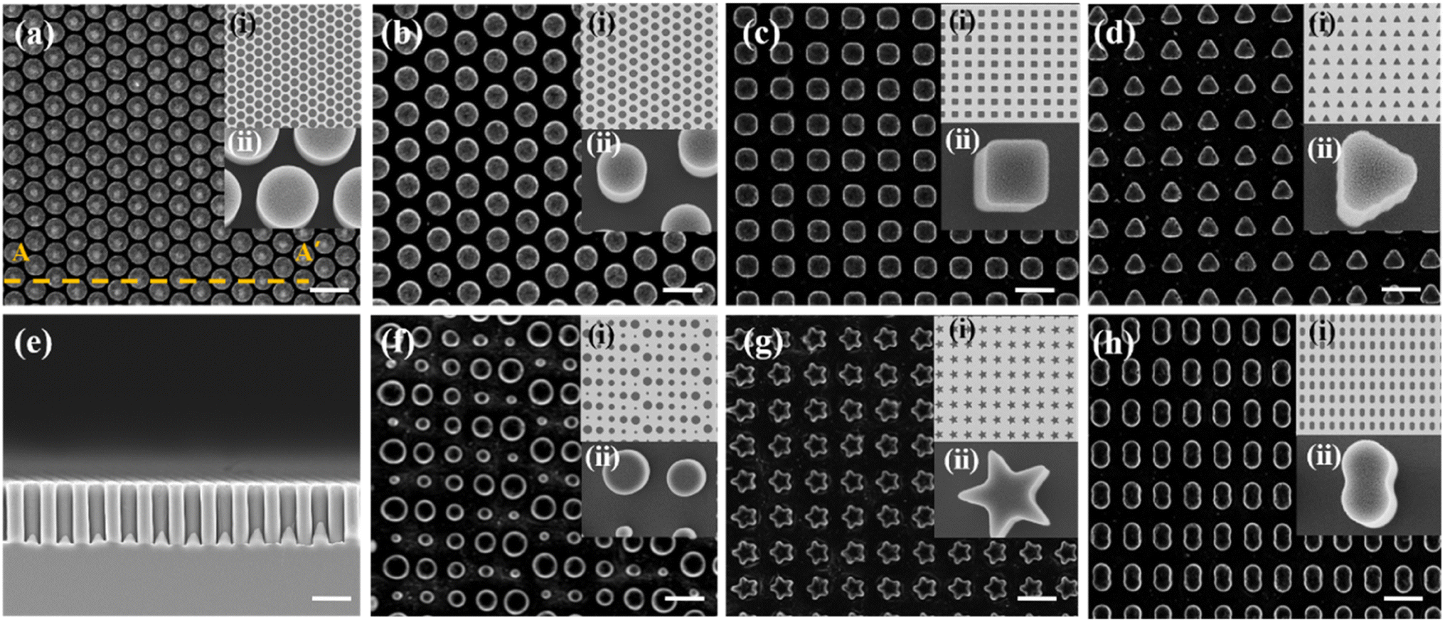 | ||
| Fig. 3 Nano/micro hybrid structures with arbitrary geometries fabricated by the “one-step MacEtch” approach we proposed. (a) Densely arranged circular structures with a pitch of 4 μm and a diameter of 3 μm. (e) Cross-sectional SEM image of the yellow dotted line from A to A′ in panel (a). (b–d) Commonly used structures: circular (b) square (c) and triangle (d) shape, the pitch of the structures was 5 μm, and the feature size was 3 μm. (f) Circular structures with varied diameter from 2 μm to 6 μm. (g) “Pentagram”-shaped structures with a pitch of 10 μm. (h) “Peanut” -shaped structures with a pitch of 10 μm. The inset (i) shows the SEM image of the corresponding arbitrary geometry after ion beam etching and the inset (ii) shows the SEM image of the nanostructure on the top of micropillars. | ||
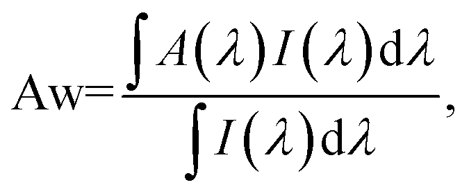
To compare the differences in optical properties between nano/micro hybrid structures and mono-micro structures, Si micropillar arrays with a hexagonal arrangement were fabricated by using a photolithography process and the Bosch process of Si deep RIE, as shown in Fig. 4. The Bosch process is a high-aspect-ratio plasma etching process. The process consists of isotropic cyclic etching and fluorocarbon protective film deposition via fast gas switching. The SF6 plasma cycle etches the Si and the C4F8 plasma cycle produces a protective layer. Each micropillar fabricated has a diameter of 2.5 μm and a pitch of 5 μm, as shown in Fig. 4a. The etching speed of the Bosch process we set is approximately 2 μm min−1. By adjusting the processing time, micropillars with lengths ranging from 5 to 20 μm were fabricated as shown in Fig. 4a–d. A 200 nm thick layer of aluminum was deposited on the rear surface of the Si wafer to act as a rear reflector. The reflectance and absorbance of the micropillars were measured with a UV-vis-NIR spectrophotometer in the wavelength range of 400–1100 nm. As shown in Fig. 4e, the reflection of the micropillars has been reduced significantly compared to that of the planar Si substrate, which is mainly attributed to the micropillars that acted as a buffer layer, narrowing a large difference in the effective refractive indices between air and the substrate. The reflectance gradually decreases as the length of the micropillar increases. This is because the amount of incident light entering the wafer increases as the length of the micropillar increases, allowing the wafer to absorb more light. Besides, the light path length increased with increasing pillar height, which also enhanced the light trapping effect. At larger lengths, the reflection spectrum is characterized by spectral oscillations, attributed to Fabry–Perot (FP) resonances of the finite length geometries.39 These Fabry–Perot oscillations are a general characteristic of a two-interfaces system and can be observed in the uniform slab geometry as well as in the arrays of pillars.40 The weighted absorption (Aw) values with the AM 1.5 G spectrum for all the surfaces are shown in Fig. 4f, Aw is calculated by averaging the absorption using:
 | (1) |
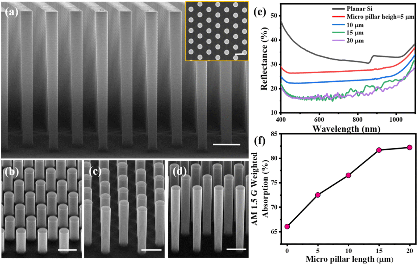 | ||
| Fig. 4 Characterization of micropillar arrays of different heights. (a) Cross-sectional SEM images of micropillar arrays of 20 μm height. The inset shows the top-view SEM image of micropillar arrays. Cross-sectional SEM images of micropillar arrays of different heights: (b) 5 μm, (c) 10 μm, and (d) 15 μm. The scale bar in the SEM images is 5 μm. (e) The reflection spectrums of planar Si and micropillar arrays of different heights. (f) The AM 1.5 G weighted absorption for planar Si and micropillar arrays of different heights. All scale bars in the SEM images are 5 μm. | ||
Fig. 5a shows the optical images of planar Si, mono micropillar arrays and nano/micro hybrid structures. Here, both the mono micropillar structures and the nano/micro hybrid structures are arranged in a hexagonal shape, as shown in Fig. 5a. The morphological parameters are the same for both the micropillar arrays and the nano/micro hybrid structures. The height is 20 μm, the period is 5 μm, and the diameter is 2.5 μm. The optical images of the micropillar arrays exhibit colors owing to diffracted light, implying that a considerable amount of light was reflected from the top surface. This observation indicates that micropillar arrays cannot completely absorb the incident light, despite the pillar height being 20 μm and the absorption reaching a maximum. By contrast, the optical image of the nano/micro hybrid structures is completely black, confirming that the surface reflection of light is almost zero. This can also be confirmed by the reflectance shown in Fig. 5b. The average reflectivity of the Si plane is higher than 30%, and the lowest average reflectivity of the micropillars is between 15–20%, and in contrast, that of the nano/micro hybrid structures was nearly 1%. This significant reflectivity reduction of the nano/micro hybrid structures relative to the mono micropillar arrays is due to the energy decay in the surface light reflections and optical path length extension through the internal refraction and transmission processes. As a result, the employment of surface textures can effectively suppress such reflection losses by permitting more incident light to enter the structure and multi-reflect along the depth direction.41 As far as the optical path length is concerned, our nano/micro hybrid structures are significantly larger than the mono micropillar arrays, which implies that light waves will have more opportunities to achieve a coupling decay with Si. The employment of a structure that induces multiple internal reflections, light refraction, and transmission effects can facilitate such a coupling decay process.42 As a result, nano/micro hybrid structures with a smaller smooth area on top can trap enhanced incident light, leading to constant attenuation through the consecutive interactions of light and Si within the structure. On the other hand, the reduction in reflection can also be explained by the mitigation of the refractive index mismatch.43 Incident light strikes the subwavelength structure as if it comes across a thin antireflective layer with a refractive index between that of air and Si, increasing the amount of light entering the structure.44 Therefore, the nanostructures on top of the micropillars make the reflection decrease effectively. Since the index-matching is independent of wavelength essentially, the reflection can be suppressed over a wide range of wavelengths. In addition, three-dimensional FDTD simulations were performed to simulate the reflection of nano/micro hybrid arrays. The reflection spectra of all the fabricated nano/micro hybrid arrays matched well with the simulated absorption spectra in the wavelength range of 500–1100 nm. However, an oscillation was observed in the simulated absorption spectra, showing a difference from the experimental spectra. The FDTD simulation uses a light source with high coherence, and thus the interference effect of the reflected light increases significantly during the simulation of a spectrum for a highly periodical structure. Fig. 5c shows the integral of the absorption spectra of each structure under AM 1.5 G illumination. The absorption of the nano/micro hybrid structure is 98.82%, confirming that this structure absorbs the highest amount of incident light, which is expected to improve the conversion efficiency.
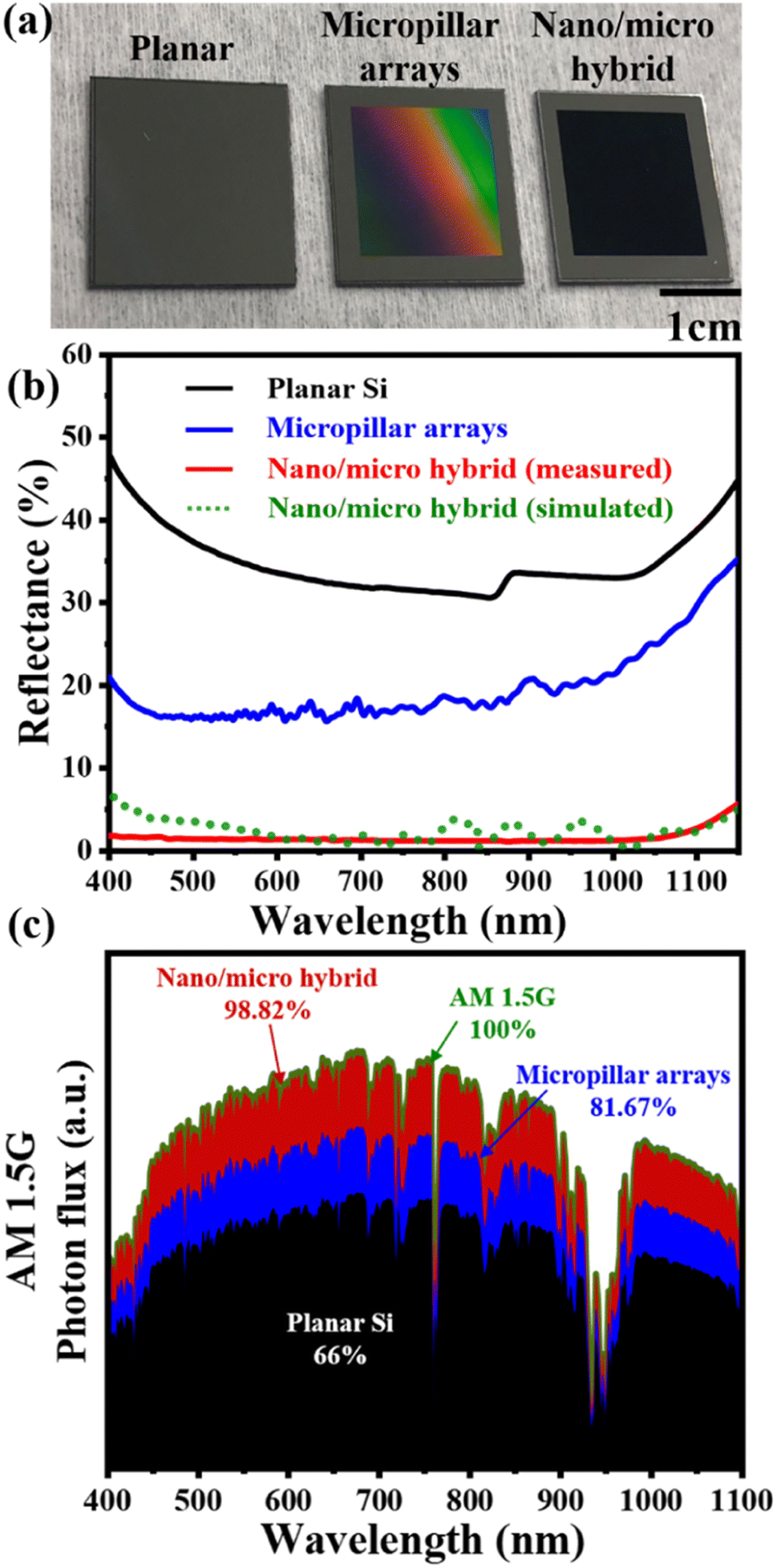 | ||
| Fig. 5 Comparison of the optical properties of planar Si, mono micropillar arrays and nano/micro hybrid structures. (a) Photograph of samples with and without etching: from left to right are plane single-crystalline Si without etching, single-crystalline Si planar with micropillars, and nano/micro hybrid structures. (b) Reflectance spectra of planar Si, micropillar arrays, and nano/micro hybrid structures. (c) Spectral distribution of absorbed photons of planar Si (black), micro pillar arrays (blue), nano/micro hybrid structures (red), and AM 1.5 G spectrum (green). | ||
To reveal the mechanism for this broadband high absorption, the electromagnetic field distribution inside the hybrid structures was simulated using the FDTD method. Fig. 6 shows the top and side views of the electric field distribution inside the nano/micro hybrid structures with incident wavelengths of 450, 650, 850, and 1050 nm. An enhanced electric field can be observed on top of the nano/micro hybrid structures, demonstrating that surface recombination loss did not impact absorption much when the thin nanostructured layer is ∼50 nm, as we fabricated. In addition, the electric field intensity was higher in the gaps between the micropillars, suggesting that more incident light could be trapped for higher optoelectronic conversion. This is because the field pattern in the micropillars was similar to that of the optical modes in cylindrical waveguides due to the geometry, and the periodic array can serve as a grating that ensures phase-matched coupling of a normally incident plane wave to a waveguided mode of the Si layer.45 Since Si has a low absorption coefficient for near-infrared incident light, when the wavelength is greater than 1000 nm, some of the light is still reflected despite the redistribution effect caused by the nanostructure that can increase the optical path length, resulting in an enhanced electric field outside the structure, as shown in Fig. 6d.
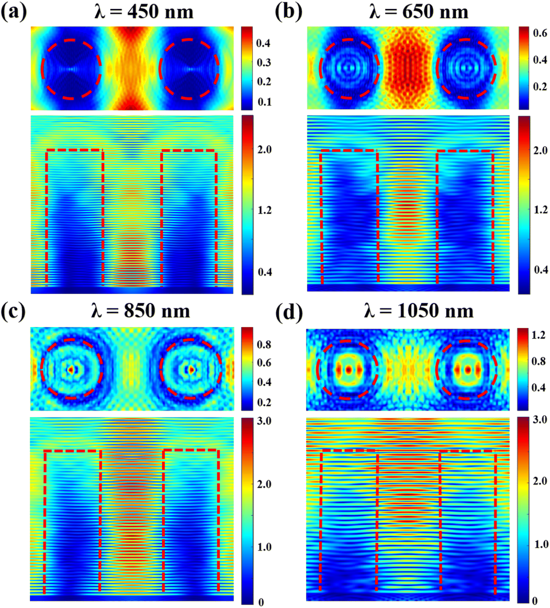 | ||
| Fig. 6 Top and side view of electric field |E| distributions of nano/micro hybrid structures at different absorption wavelengths: (a) 450 nm, (b) 650 nm, (c) 850 nm, and (d) 1050 nm. The period of the micropillar is 5 μm, and the diameter is 2.5 μm. | ||
After well verifying that the nano/micro hybrid structure arrays have promising light absorption properties, we applied them to a photovoltaic device, as shown in Fig. 7. Here, we chose pillars with 2.5 μm diameter and 5 μm pitch for this application. The schematic of a nano/micro hybrid structure array-based solar cell is shown in Fig. 7a, and Fig. 7b and c show SEM images of nano/micro hybrid structures. Note that the Si surface below the top electrode is not textured and always retains a flat surface, which is advantageous for good contact and better conductivity. The corresponding photovoltaic properties are shown in Fig. 7d. This reveals that the best performance of the nano/micro hybrid solar cells achieved a photovoltaic conversion efficiency (Eff) of 14.7%, along with an open-circuit voltage (Voc), short-circuit current density (Jsc), and fill factor (FF) of 587.5 mV, 34.43 mA cm−2, and 72.7%, respectively. The efficiency of this hybrid cell increased by approximately 19.5% and 11.4% compared to those of the planar Si solar cell (Eff = 12.3%) and the micropillar solar cell (Eff = 13.2%), which can mainly be attributed to the enhanced light trapping efficiency of top nanostructures. The Jsc value of the nano/micro hybrid solar cells was 20.3% and 6.9% higher than those of the planar (28.61 mA cm−2) and micropillars (32.21 mA cm−2) devices, and this shows that the benefit of light absorption surpassed the disadvantage of recombination loss. However, regardless of the structure, the Voc and FF are similar. These similar Voc and FF are due to the thin nanostructured layers that minimize the effect of surface recombination occurring in the nanostructure. Therefore, the hybrid cell has balanced surface recombination, light absorption, and carrier separation and can yield high Eff. As shown in Fig. 7e, the external quantum efficiency (EQE) of the nano/micro hybrid solar cell in the short wavelength range (600 nm) increases to more than 92% because of the increased absorption by the nanostructure. Compared to planar and micropillar solar cells, the hybrid cell's EQE value increased by approximately 25% and 9% at wavelengths between 600 nm and 900 nm, which is consistent with the testing result from the reflection spectra (Fig. 5b). Furthermore, the improved EQE value at short-wavelengths (400–550 nm) indicates a much better response to blue light (high energy photons) than planar and micropillar devices which are caused not only by the increased light absorption but also by the effective carrier separation of the radial junction in nano/micro hybrid solar cells. This is because the radial junction allows for high device efficiency by decoupling the axis of light absorption and the axis of charge carrier separation. Therefore, in a radial junction solar cell, light absorption, especially the absorption of blue light (high energy photons) will directly reflect the degree of charge carrier separation, and both can be optimized separately to achieve the best performance of nano/micro hybrid solar cells. Light is absorbed along the main axis of the hybrid structure, while charge carrier separation takes place in the radial direction which is just tens of nanometers thick. Both charge carrier separation and light absorption can separately be optimized.
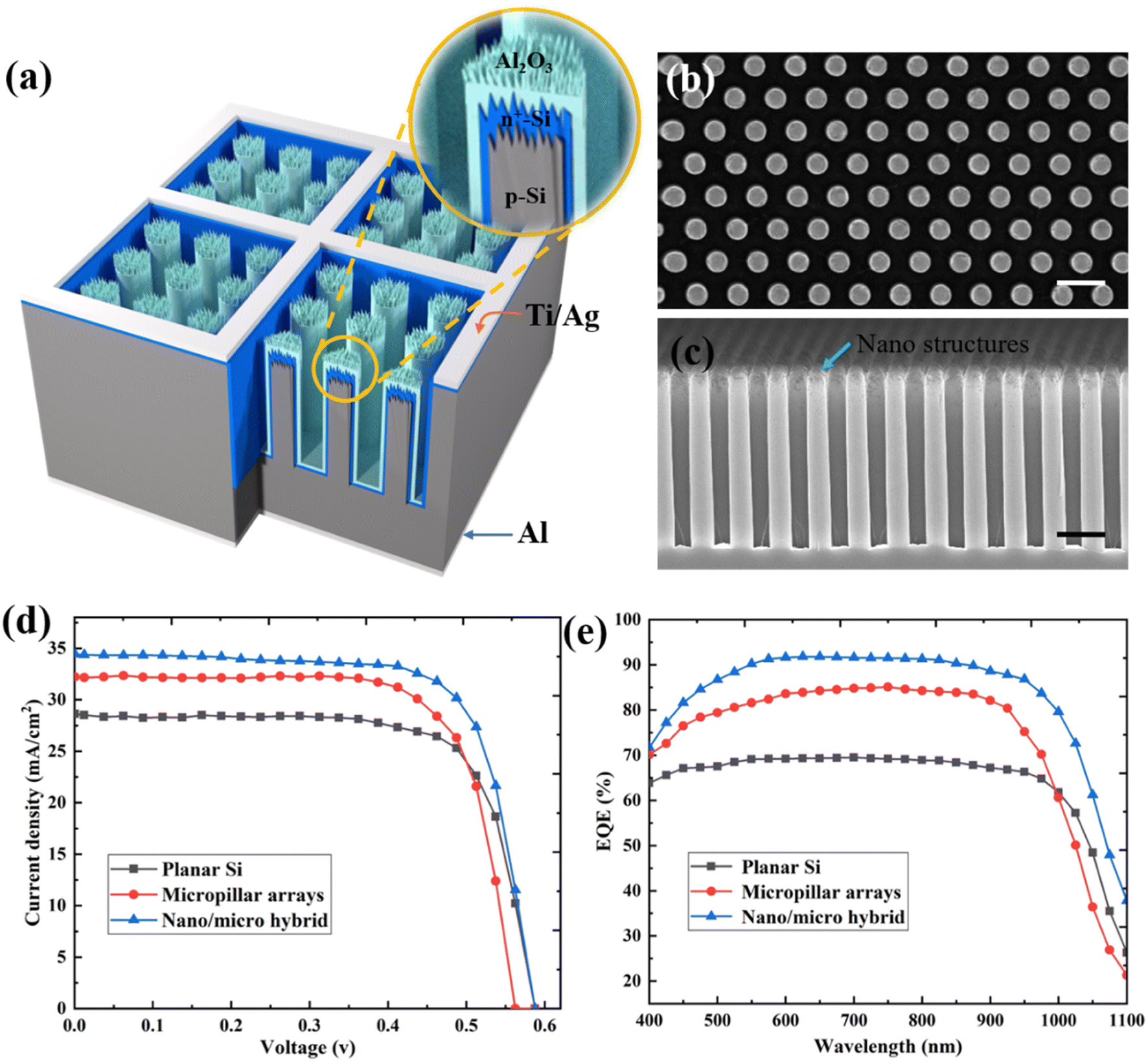 | ||
| Fig. 7 Application of Si nano/micro hybrid structure arrays in solar cells. (a) Schematic illustration of a nano/micro hybrid structure array-based solar cell. (b and c) SEM images of 3D Si nano/micro hybrid structure arrays with 2.5 μm diameter and 5 μm pitch: (b) top view and (c) cross-sectional view. (d) Current density–voltage characteristics of planar, micropillar, and nano/micro hybrid solar cells under an illumination of AM 1.5 G. (e) External quantum efficiencies of planar, micropillar, and nano/micro hybrid solar cells. All scale bars in the SEM images are 6 μm. | ||
Conclusion
In summary, we proposed a “one-step MacEtch” method to fabricate nano/micro hybrid structures, which are extremely challenging to be fabricated by other methods. These hybrid structure arrays showed a high integrated absorption of 98.82% in the broad wavelength region (400–1100 nm), significantly higher than that of planar or micropillar array structures. Finally, we applied Si nano/micro hybrid structure arrays to photovoltaics, showing that the efficiency of this hybrid cell increased by approximately 19.5% and 11.4% compared to those of the planar Si solar cell (Eff = 12.3%) and the micropillar solar cell (Eff = 13.2%). It indicates that the Si nano/micro hybrid structure arrays fabricated by the “one-step MacEtch” approach we proposed can have potential applications in high-performance photovoltaic devices.Experiments
Fabrication of micropillar arrays
The ICP-“Bosch” process for deep Si etching: chamber pressure was 3 mTorr, platen RF power was 12 W, and top coil power was kept at 650 W. In the passivation cycle, the C4F8 flow rate was 85 sccm, passivation time was 6 s, and delay time was 0.5 s. In the etching cycle, the SF6 flow rate was 135 sccm, etch time was 9 s, and delay time was 0.5 s. The etching rate was maintained at 2 μm min−1.The conventional process for the fabrication of nano/micro hybrid structures
The conventional process (as shown in Fig. 1a) starts from a single crystal Si substrate coated with a photoresist. After that, high aspect ratio Si micropillar arrays were fabricated using a photolithography process and deep reactive-ion etching (DRIE). After fabricating the micropillars, an additional C4F8 gas flow formed a non-conductive fluorocarbon polymer film as a passivation layer over the entire surface of the micropillar arrays. Next, the photoresist on top of the micropillars was lifted off to expose Si on top of the micropillars. Then, two-dimensional (2D) polystyrene (PS) nanoparticles were lifted onto the microscale silica patterns, followed by an oxygen plasma treatment. Finally, reactive ion etching (RIE) was used to shape nanostructures on top of the micro pillars, followed by the removal of polymer residues.Fabrication of nano/micro hybrid structures
4-Inch double-side polished P-type 〈100〉-oriented Czochralski (CZ) Si wafers with a resistivity of 1–20 Ω cm and a thickness of ∼500 μm were used as the starting substrate to fabricate 3D hybrid nano/microstructures. First, a 3 nm Ti adhesion film and 20 nm Au catalyst film were deposited onto the Si substrate by using a magnetron sputtering system (ACS-4000, ULVAC Corporation, Japan). The working pressure was maintained at 4.5 × 10⁻⁶ Torr, and the chamber temperature was kept at 25 °C throughout the deposition process. A single layer of commercially available NR1500 negative photoresist was spin-coated on the Ti/Au layer and baked on a hot plate at 150 °C for 2 min. The thickness of the photoresist film was about 1.4 μm. Then, hard contact mode UV lithography and resist development were performed to define etching patterns onto the resist. At this point, the substrate was treated with mild oxygen plasma to remove the residual resist. Sequentially, the ion beam etching technique was used to transfer the resist pattern onto the Ti/Au layer, and the residual resist was then chemically removed using acetone. The specific process parameters for ion beam etching were as follows: working pressure: −2 Pa, etching temperature: −15 °C, beam current: 90 mA, accelerating voltage: 160 V, and gas flow of argon: 17 sccm. All metal films were deposited at a sputtering rate of 1 Å s−1. The Ti/Au (3/20 nm) film with microstructures that serves as a local cathode for the MacEtch process was then created. Finally, in a mixed solution containing hydrofluoric acid (HF), hydrogen peroxide (H2O2), and DI water with a molar ratio of 4.8![[thin space (1/6-em)]](https://www.rsc.org/images/entities/char_2009.gif) :0.12:50, the Si beneath Ti/Au microstructures was etched away by vertical directionally controlled MacEtch, forming anisotropic high aspect ratio Si microstructures. The adherent layer of the Ti film was also dissolved in the solution at the same time. And the Au particles implanted into Si by physical bombardment with the ion beam would be unbound and MacEtched isotropically in the vicinity of the Si surface, thus forming nanostructures simultaneously. After the nano/micro hybrid structure arrays were fabricated, the catalyst film of Au was removed by using a mixed aqueous solution of KI/I2/H2O (weight ratio = 4:1:10).
:0.12:50, the Si beneath Ti/Au microstructures was etched away by vertical directionally controlled MacEtch, forming anisotropic high aspect ratio Si microstructures. The adherent layer of the Ti film was also dissolved in the solution at the same time. And the Au particles implanted into Si by physical bombardment with the ion beam would be unbound and MacEtched isotropically in the vicinity of the Si surface, thus forming nanostructures simultaneously. After the nano/micro hybrid structure arrays were fabricated, the catalyst film of Au was removed by using a mixed aqueous solution of KI/I2/H2O (weight ratio = 4:1:10).
Fabrication of nano/micro hybrid structures based on photovoltaic devices
When the nano/micro hybrid structure arrays were obtained and cleaned by the standard RCA process, to form an emitter layer on the surface of the nano/micro hybrid structure arrays, all samples were spin-coated and chemically doped with the phosphorous-containing spin-on-dopant (SOD) to achieve an n+/p junction. The whole diffusion process was implemented under an atmosphere of O2 (300 sccm) and N2 (1100 sccm) for 30 min with an annealing temperature of 900 °C. After this diffusion process, a thin layer of phosphosilicate glass (PSG) with a uniform thickness of 30–40 nm, which can also be used directly as a passivation layer, was formed on the surface of the nano/micro hybrid structures. Then, an Al2O3 film was deposited as a passivation layer using Al(CH3)3 (TMA) and deionized (DI) water in a hot-wall atomic layer deposition system (Picosun R200, Espoo, Finland) at a deposition temperature of 300 °C. TMA (Sigma Aldrich, St. Louis, MO, USA) was used as a precursor, and DI water was used as the oxidant source during the ALD process. The TMA reactant exposure time, N2 purge time after TMA reactant exposure, water exposure time, and N2 purge time after H2O reactant exposure were 0.5 s, 2 s, 0.5 s, and 2 s, respectively. The growth rate of Al2O3 films was 0.089 nm per cycle. The samples were treated with 562 ALD cycles, and the corresponding Al2O3 film thickness was 50 nm. Electron-beam evaporation was carried out to deposit the top metal electrode contact (20 nm Ti/400 nm Ag) with the electrode pattern pre-defined by conventional photolithography, followed by the lift-off process. After that, 300 nm aluminum (Al) was fabricated as the bottom metal electrode contact by magnetron sputtering deposition. Finally, the samples were cut into small cells with an area of 22 × 22 mm2 for subsequent testing, and these devices were finally annealed at 400 °C for 10 min under a H2 atmosphere for the formation of ohmic contact.Simulation
FDTD simulations were carried out using the Lumerical FDTD software package. An ultrafine mesh size of 2 nm was used in all the simulations. Two monitors were used to calculate the reflection spectra and the electric field distribution. The nano/micro hybrid structures were constructed using a 3D rectangular simulation region. To construct the hexagonal structure, one nano/micro hybrid pillar was placed in the center and four nano/micro hybrid pillars were located around it at each corner of the simulation area. The Si substrate at the bottom was placed underneath the hybrid structures. Periodic boundary conditions were used to obtain a periodic array in x- and y-directions. Perfectly matched layers (PML) were used along the z-direction. The Si material was modeled from the Palik material data provided by Lumerical. The simulations were performed in the wavelength range of 400–1100 nm using a plane-wave light source.Reflectance
The reflectance of the samples was measured by using a UV-vis-NIR spectrophotometer (Shimadzu UV 3600 plus, Japan) equipped with an integrating sphere with 2.0 nanometer spectral bandwidth. The inner diameter of the integrating sphere is 60 mm, and the inner layer material is BaSO4. The light measuring range is 400–1100 nm. Before testing the samples, we used BaSO4 as a whiteboard to perform the baseline calibration. Then, the reflectance measurement of the planar Si and the structured surface was performed with BaSO4 as a reference. The reflectance was collected by using an integrating sphere.Characterization of fabricated solar cell devices
The surface morphologies of the samples with different Si nano/microstructure arrays were investigated by using a scanning electron microscope (SEM, Zeiss SUPRA-V55). Light J–V curves of solar cell performances were obtained under a simulated AM 1.5 G (i.e., 1000 W m−2 at 25 °C) spectrum sunlight illumination by using a solar simulator (Newport Oriel Instruments) and the effective illumination area was 7 mm × 7 mm. External quantum efficiency (EQE) was measured using a Xe light source and a monochromator with a wavelength range of 400–1100 nm.Author contributions
H. Li and C. Xie developed the original ideas. X. Zhang and H. Li contributed to the paper writing. X. Zhang, C. Yao, J. Niu, and H. Li carried out most of the experimental work. Y. Liu optimized the fabrication steps for ion beam etching. H. Li and C. Xie assisted with some experiments and data analysis. All authors read and discussed the manuscript.Conflicts of interest
The authors declare that they have no known competing financial interests or personal relationships that could have appeared to influence the work reported in this paper.Acknowledgements
This work was carried out with the financial support of the National Natural Science Foundation of China (GrantNo. 61804169) and the National Key Research and Development Program of China (Grant No. 2017YFA0206002). The authors would like to acknowledge the National Center for Nanoscience and Technology (NCNST) for EDS facilities. The authors thank Kaiping Zhang for UV lithography and Xueqin Lu for SEM characterization.References
- J. An, X. Zhao, Y. Zhang, M. Liu, J. Yuan, X. Sun, Z. Zhang, B. Wang, S. Li and D. Li, Adv. Funct. Mater., 2021, 2110119 Search PubMed.
- J. Cheng, C. Wang, X. Zou and L. Liao, Adv. Opt. Mater., 2019, 7, 1800441 CrossRef.
- M. Widmann, M. Niethammer, D. Y. Fedyanin, I. A. Khramtsov, T. Rendler, I. D. Booker, J. Ul Hassan, N. Morioka, Y.-C. Chen and I. G. Ivanov, Nano Lett., 2019, 19, 7173–7180 CrossRef CAS.
- Y. A. Bioud, A. Boucherif, M. Myronov, A. Soltani, G. Patriarche, N. Braidy, M. Jellite, D. Drouin and R. Arès, Nat. Commun., 2019, 10, 1–12 CrossRef CAS PubMed.
- S. Bhattacharya and S. John, Sci. Rep., 2019, 9, 1–15 CrossRef.
- W. Vijselaar, P. Westerik, J. Veerbeek, R. M. Tiggelaar, E. Berenschot, N. R. Tas, H. Gardeniers and J. Huskens, Nat. Energy., 2018, 3, 185–192 CrossRef CAS.
- C. N. Lau, M. W. Bockrath, K. F. Mak and F. Zhang, Nature, 2022, 602, 41–50 CrossRef CAS PubMed.
- C. Huo, J. Wang, H. Fu, X. Li, Y. Yang, H. Wang, A. Mateen, G. Farid and K. Q. Peng, Adv. Funct. Mater., 2020, 30, 2005744 CrossRef CAS.
- N. Kim, D. Choi, H. Kim, H.-D. Um and K. Seo, ACS Nano, 2021, 15, 14756–14765 CrossRef CAS PubMed.
- J.-H. Chai, B. T. Wong and S. Juodkazis, Mater. Today Energy., 2020, 18, 100539 CrossRef CAS.
- V. Vendamani, S. Nageswara Rao, S. Venugopal Rao, D. Kanjilal and A. Pathak, J. Appl. Phys., 2018, 123, 014301 CrossRef.
- C. Yao, Y. Zhao, X. Zhang, H. Li and C. Xie, Results Phys., 2021, 31, 105018 CrossRef.
- D. Kumar, S. K. Srivastava, P. Singh, M. Husain and V. Kumar, Sol. Energy Mater. Sol. Cells, 2011, 95, 215–218 CrossRef CAS.
- Y. Cui, J. Zhang, H. He and G. Qian, Chem. Soc. Rev., 2018, 47, 5740–5785 RSC.
- R. Elbersen, W. Vijselaar, R. M. Tiggelaar, H. Gardeniers and J. Huskens, Adv. Mater., 2015, 27, 6781–6796 CrossRef CAS PubMed.
- S. Sajid, A. M. Elseman, J. Ji, S. Dou, D. Wei, H. Huang, P. Cui, W. Xi, L. Chu and Y. Li, Nano-Micro Lett., 2018, 10, 1–11 CrossRef PubMed.
- W. Huang, P. Hang, Y. Wang, K. Wang, S. Han, Z. Chen, W. Peng, Y. Zhu, M. Xu and Y. Zhang, Nano Energy, 2020, 73, 104790 CrossRef CAS.
- Z. Li, B. Corbett, A. Gocalinska, E. Pelucchi, W. Chen, K. Ryan, P. Khan, C. Silien, H. Xu and N. Liu, Light: Sci. Appl., 2020, 9, 1–10 CrossRef.
- C. Zhang, D. A. Mcadams and J. C. Grunlan, Adv. Mater., 2016, 28, 6292–6321 CrossRef CAS PubMed.
- T. Wang, D. Huang, Z. Yang, S. Xu, G. He, X. Li, N. Hu, G. Yin, D. He and L. Zhang, Nano-Micro Lett., 2016, 8, 95–119 CrossRef PubMed.
- W. Yang, J. Chen, Y. Zhang, Y. Zhang, J. H. He and X. Fang, Adv. Funct. Mater., 2019, 29, 1808182 CrossRef.
- J. Chen, W. Ouyang, W. Yang, J. H. He and X. Fang, Adv. Funct. Mater., 2020, 30, 1909909 CrossRef CAS.
- Y. Li, Q. Chen, D. He and J. Li, Nano Energy, 2014, 7, 10–24 CrossRef CAS.
- H. C. Fu, V. Ramalingam, H. Kim, C. H. Lin, X. Fang, H. N. Alshareef and J. H. He, Adv. Energy Mater., 2019, 9, 1900180 CrossRef.
- Z. Zhang, T. Martinsen, G. Liu, M. Tayyib, D. Cui, M. J. de Boer, F. Karlsen, H. Jakobsen, C. Xue and K. Wang, Adv. Opt. Mater., 2020, 8, 2000668 CrossRef CAS.
- I. R. Putra, J.-Y. Li and C.-Y. Chen, Appl. Surf. Sci., 2019, 478, 725–732 CrossRef CAS.
- J. Xu, C. Chen, C. Liu, J. Chen, Z. Liu, X. Yuan and H. Li, Sol. Energy Mater. Sol. Cells, 2021, 233, 111409 CrossRef CAS.
- G. Oehrlein, R. Tromp, Y. Lee and E. Petrillo, Appl. Phys. Lett., 1984, 45, 420–422 CrossRef CAS.
- H.-D. Um, N. Kim, K. Lee, I. Hwang, J. Hoon Seo, Y. J. Yu, P. Duane, M. Wober and K. Seo, Sci. Rep., 2015, 5, 1–11 Search PubMed.
- Z. Huang, N. Geyer, P. Werner, J. De Boor and U. Gösele, Adv. Mater., 2011, 23, 285–308 CrossRef CAS PubMed.
- X. Li and P. Bohn, Appl. Phys. Lett., 2000, 77, 2572–2574 CrossRef CAS.
- H. Li, J. Niu, G. Wang, E. Wang and C. Xie, ACS Appl. Electron. Mater., 2019, 1, 1070–1075 CrossRef CAS.
- K. Lee, I. Hwang, N. Kim, D. Choi, H.-D. Um, S. Kim and K. Seo, Nanoscale, 2016, 8, 14473–14479 RSC.
- H. Lin, F. Wu, P. Gao and W. Shen, ACS Appl. Energy Mater., 2019, 2, 5871–5876 CrossRef CAS.
- R. P. Srivastava and D. Y. Khang, Adv. Mater., 2021, 33, 2005932 CrossRef CAS PubMed.
- H. Han, Z. Huang and W. Lee, Nano today, 2014, 9, 271–304 CrossRef CAS.
- D. Zhang, S. Jiang, K. Tao, R. Jia, H. Ge, X. Li, B. Wang, M. Li, Z. Ji and Z. Gao, Sol. Energy Mater. Sol. Cells, 2021, 230, 111200 CrossRef CAS.
- W. Liu, S. Xiang, X. Liu and B. Yang, ACS Nano, 2020, 14, 9166–9175 CrossRef CAS PubMed.
- B. Wang, P. Yu, W. Wang, X. Zhang, H. C. Kuo, H. Xu and Z. M. Wang, Adv. Opt. Mater., 2021, 9, 2001520 CrossRef CAS.
- M.-H. Lu, L. Feng and Y.-F. Chen, Mater. Today, 2009, 12, 34–42 CrossRef CAS.
- J. Flick, N. Rivera and P. Narang, Nanophotonics, 2018, 7, 1479–1501 CAS.
- P. Vasa and C. Lienau, ACS Photonics, 2018, 5, 2–23 CrossRef CAS.
- B. Chen, X. Zheng, Y. Bai, N. P. Padture and J. Huang, Adv. Energy Mater., 2017, 7, 1602400 CrossRef.
- H.-P. Wang, D. Periyanagounder, A.-C. Li and J.-H. He, IEEE Access, 2018, 7, 19395–19400 Search PubMed.
- M. L. Brongersma, Y. Cui and S. Fan, Nat. Mater., 2014, 13, 451–460 CrossRef CAS PubMed.
| This journal is © The Royal Society of Chemistry 2023 |