
 Open Access Article
 This Open Access Article is licensed under a Creative Commons Attribution-Non Commercial 3.0 Unported Licence
A polarization-sensitive photothermoelectric photodetector based on mixed-dimensional SWCNT–MoS2 heterostructures†
Pei-Yu
Huang
a,
Hong-Ji
Chen
a,
Jing-Kai
Qin
 *a,
Liang
Zhen
ab and
Cheng-Yan
Xu
*ab
*a,
Liang
Zhen
ab and
Cheng-Yan
Xu
*ab
aSauvage Laboratory for Smart Materials, School of Materials Science and Engineering, Harbin Institute of Technology (Shenzhen), Shenzhen 518055, China. E-mail: jk.qin@hit.edu.cn; cy_xu@hit.edu.cn
bMOE Key Laboratory of Micro-System and Micro-Structures Manufacturing, Harbin Institute of Technology, Harbin 150080, China
First published on 25th September 2022
Abstract
Mixed-dimensional van der Waals (vdW) integration has been demonstrated to be effective for the modulation of the physical properties of homogeneous materials. Herein, we reported the enhancement of photothermal conversion and decrease of thermal conductivity in metallic single-walled carbon nanotube (SWCNT) films with the integration of chemical vapor deposition-grown monolayer MoS2 films. The induced temperature gradient in SWCNT–MoS2 hybrid films drives carrier diffusion to generate photocurrent via the photothermoelectric (PTE) effect, and a self-powered photodetector working in the visible band range from 405 to 785 nm was demonstrated. The maximum responsivity of the device increases by 6 times compared to that of the SWCNT counterpart. More importantly, the mixed-dimensional device exhibits polarization-dependent photogeneration, showing a large anisotropy ratio of 1.55. This work paves a way for developing high-performance, polarization-sensitive photodetectors by mixed-dimensional integration.
Introduction
Photothermoelectric (PTE) photodetectors based on the Seebeck effect have attracted extensive attention due to advantages such as broadband spectral response,1 room temperature operation,2 self-power capability,3etc. In principle, a typical PTE process relies on the photothermal conversion and thermoelectrical effect. Light illumination would induce a local temperature rise of the material, thus contributing to a temperature gradient across the sample. The excited carriers will diffuse directionally from the hot terminal to the cold terminal, resulting in an electric potential difference. The photovoltage Vph originating from the PTE effect can be described as:| Vph = ∫S(x)ΔT(x)dx | (1) |
Low-dimensional materials such as graphene,5,6 WSe2,7 black phosphorus (B-P),8 and single-walled carbon nanotubes (SWCNTs)9 were proven to have a large PTE effect. Among them, SWCNTs exhibit broad optical absorption (∼200 nm to 200 μm),10 high electron mobility (∼105 cm2 V−1 s−1),11 and a relatively large Seebeck coefficient (∼+260 μV K−1),12 and thus they are regarded as an ideal candidate for fabricating state-of-the-art PTE photodetectors. For example, Martel et al. investigated the PTE effect of suspended SWCNT films in a vacuum under highly localized illumination.13 They demonstrated that the freestanding SWCNT films exhibit a position-sensitive photoresponsivity of 0.3 V W−1, which is independent of the SWCNT–metal contact barriers. However, the performance improvement of SWCNT-based PTE photodetectors still faces great challenges, since the intrinsic high thermal conductivity and low optical absorption of ultra-thin SWCNT films usually cause a small temperature gradient across the device channel.
The hybridization of two-dimensional (2D) functional materials is effective for the modulation of the physical properties of SWCNTs,14–18 offering new opportunities to design advanced devices with high performance and multifunctionality. Benefiting from the direct band gap and broadband light absorption in the visible region, monolayer MoS2 shows great potential for hybridization to improve the performance of SWCNT-based photodetectors. In this work, we directly synthesized atomically thin MoS2 monolayers on highly aligned SWCNT films, and demonstrated that the hybrid films can work as the channel material for constructing a high-performance PTE photodetector with polarization sensitivity. We systematically investigated the optoelectronic properties of the hybrid films via scanning photocurrent microscopy (SPCM). Owing to the enhancement of light absorption and the decrease in thermal conductivity, the responsivity of the self-powered PTE photodetector based on SWCNT–MoS2 hybrid films increases by 6 times compared to that of the SWCNT counterpart. Attributed to the anisotropic optical absorption of the hybrid films, the device also demonstrated a strong polarization-sensitive photoresponse in the visible band, showing a large anisotropy ratio of 1.55 under 532 nm light illumination.
Experimental section
Preparation of aligned SWCNT films
We prepared highly aligned SWCNT films on a SiO2/Si substrate using a self-assembly approach reported in previous work.19 Metallic SWCNTs with an average diameter of 1.4 nm were purchased from Sigma-Aldrich. Sodium deoxycholate (DOC, Aladdin) was used as a surfactant for SWCNT dispersion. About 1 mg of SWCNT bundles were initially dispersed in 1% (wt/vol) DOC aqueous solution by tip sonication for 30 min. The dispersed SWCNT suspension was then diluted below the critical micelle concentration (CMC), and the final concentration of DOC was about 0.05%. Before depositing films, the SiO2/Si substrate was treated with O2 plasma to improve the hydrophilicity of the surface, which was vertically immersed in the as-prepared SWCNT suspension for 24–48 h at 0.04 MPa pressure.Growth of monolayer MoS2 on SWCNT films
Before MoS2 growth, a hydrogen annealing process was carried out to obtain a clean surface of SWCNT films. The as-fabricated SWCNT films were loaded into a tube furnace, and the temperature of the furnace was ramped to 650 °C within 10 min. The annealing process was kept for 10 min in Ar/H2. MoS2 monolayers were synthesized on SWCNT films via atmospheric pressure chemical vapor deposition (APCVD) using MoO3 and S powders as precursors (ESI Fig. S1†). 250 mg of S powder was placed in the upper stream and heated to ∼160 °C using a heating belt, while mixed powders of MoO3 (∼0.5 mg) and NaCl (∼0.5 mg) were loaded into another quartz boat. The SiO2/Si substrate coated with SWCNT films was placed 3–5 mm above the quartz boat. The growth temperature was set to be 830 °C, and 50 sccm Ar was used as the carrier gas.Materials characterization
The morphology of SWCNT–MoS2 hybrid films was obtained with an optical microscope (OM, Zeiss Axioscope 5), scanning electron microscope (SEM, Zeiss Quanta FEG 250 with 5 kV operation voltage) and atomic force microscope (AFM, Bruker Icon). The micro-Raman and micro-photoluminescence (PL) measurements were performed with a confocal microscope-based Raman spectrometer (Metatest corporation, Scan pro advance) under 532 nm. The binding energy of elements was obtained using X-ray photoelectron spectroscopy (XPS) measurements (ESCALAB 250 Xi). Before the transmission electron microscopy (TEM) measurements, the hybrid films were transferred onto microgrid-supported Cu grids via a polyvinyl alcohol (PVA) assisted transfer technique. The HADDF-STEM image and SAED patterns were collected using an FEI Talos F200s transmission electron microscope with 200 kV operation voltage.Device fabrication and measurements
The device based on SWCNT–MoS2 hybrid films was fabricated via laser direct writing, followed by the deposition of Ti/Au (10/80 nm) electrodes. Optoelectronic measurements were carried out with the assistance of a Metatest ScanPro system (Metatest corporation, Scan pro advance). A focused 532 laser was generated by a digital modulator (Coherent, OBIS), and the spot size was set to be 0.5 μm for SPCM characterization. A Keithley 2612B was used to supply the source–drain bias voltage and collect data. All the measurements were performed at atmospheric pressure and room temperature.Results and discussion
The morphology of pre-deposited SWCNT films is shown in ESI Fig. S2.† 20 μm-width SWCNT strips are regularly patterned with a spacing of 30 μm on a SiO2/Si substrate. The SEM image reveals that most of the SWCNT bundles in an individual stripe are well aligned along the axial direction of SWCNTs. From the polarized Raman spectra, we found that the Raman intensity of the characteristic peak (G band) for SWCNTs reaches the highest value with the incident light parallel to the axial direction of SWCNTs, while it decreases to the minimum value with the light along the perpendicular direction, confirming the polarization-sensitive characteristics of SWCNT films (ESI Fig. S3†). Fig. 1a and ESI Fig. S4† display the optical images of the as-fabricated SWCNT–MoS2 hybrid films. MoS2 monolayers prefer to grow on the SWCNT films and aggregate into continuous films along the parallel direction of SWCNT strips. The hydrogen annealing process plays a key role in the epitaxial growth of MoS2 monolayers on SWCNT films. Owing to the excessive nucleation sites arising from the residual surfactant and amorphous carbon, MoS2 particles randomly distributed on the entire substrate are obtained without a hydrogen annealing process (ESI Fig. S5†). Typical SEM and AFM images of the SWCNT–MoS2 hybrid structures are shown in Fig. 1b and c. The underlaying SWCNT films exhibit an undulating morphology with nanopores in the range of several hundreds of nanometers. The height of the upper MoS2 film is measured to be 0.78 nm, corresponding to the thickness of the monolayer. In the MoS2 growth process, precursors tend to be confined in the gaps and pores of SWCNT networks. It would lead to the priority nucleation of MoS2 on SWCNT films, thus resulting in the formation of MoS2 monolayers with relatively rough surface and irregular edges (ESI Fig. S6†).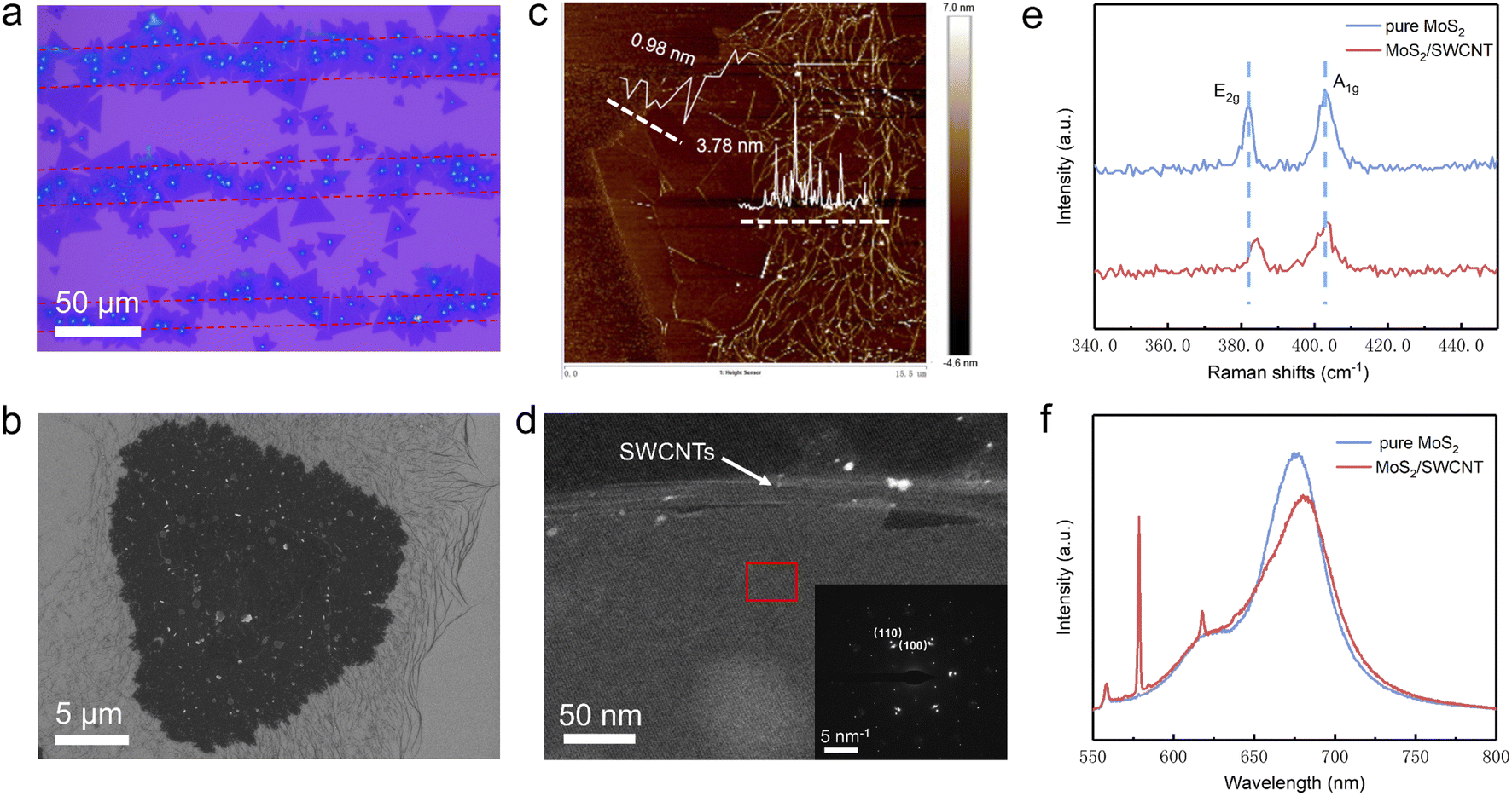 | ||
| Fig. 1 Morphology and structural characterization of SWCNT–MoS2 hybrid films. (a) OM and (b) SEM images of SWCNT–MoS2 hybrid films. (c) AFM tomography image and height profiles of SWCNT–MoS2 hybrid films. (d) HADDF-TEM image of SWCNT–MoS2 hybrid films. Inset image displays the SAED patterns of the red rectangle in (d). (e) Raman spectra and (f) PL spectra of pure MoS2 and SWCNT–MoS2 hybrid films. | ||
XPS spectrum of SWCNT–MoS2 hybrid films is shown in ESI Fig. S7.† The peaks at 229.5 and 233 eV are ascribed to the Mo4+ 3d5/2 and 3d3/2, and the peaks at 163 and 164.1 eV belong to the S 2p3/2 and 2p1/2 core levels. Note that the peak at 284.9 eV, which represents the C–C bond of SWCNTs, slightly blueshifts by 0.3 eV after MoS2 monolayer growth. This indicates that the increase of surface charge density occurs due to the electron injection from MoS2 into SWCNTs.20 TEM was carried out to identify the crystal quality of SWCNT–MoS2 hybrid films (Fig. 1d). From the HADDF-TEM image, we can clearly observe the uniform growth of MoS2 monolayers along the axial direction of the nanotube bundles. Selected-area electron diffraction (SAED) patterns show a set of hexagonally arranged spots, which are marked as MoS2 with a (100) interplanar spacing of 2.8 Å.21
Raman spectroscopy and PL microscopy were also performed to investigate the lattice vibration and optical properties of SWCNT–MoS2 hybrid films. The results are shown in Fig. 1e, f and ESI Fig. S8.† We can see that the peak position of the MoS2 E2g mode in hybrid films exhibits a relatively large redshift (∼4 cm−1) compared with the pure MoS2 monolayer, which can be ascribed to the in-plane tensile strain induced during the growth process.22 Meanwhile, the strain-caused lattice distortion would widen the band gap of the MoS2 monolayer,23 resulting in the redshift of the PL peak by 16 meV. Attributed to the electron transfer from MoS2 to SWCNTs as discussed above,24 the A1g peak of MoS2 redshifts by 0.8 cm−1, and the G mode of SWCNTs also blueshifts by 1 cm−1.
With the mixed-dimensional SWCNT–MoS2 hybrid films as the channel material, we designed a self-powered photodetector, in which the photocurrent is generated relying on the PET effect. Fig. 2a shows a schematic design of the PTE detector. The dual-channel device was fabricated along the stripe of films with Ti/Au (10/80 nm) as electrodes. The channel length and width are patterned to be 5 and 8 μm, respectively. As shown in ESI Fig. S9,† the typical linear characteristic of the Ids–Vds curve under dark conditions indicates a good ohmic contact at the electrode–channel heterointerface. When a 532 nm laser irradiates the channel of the device, an obvious photocurrent was generated without external bias, showing a typical self-powered characteristic. The short-circuit current (Isc) rises from 22 to 49 nA with the increase of light power from 0.26 to 0.59 mW, and the corresponding open-circuit voltage (Voc) also increases from 0.9 to 2.1 mV (Fig. 2b). We further evaluated the device performance under laser illumination with different wavelengths (405, 532, and 785 nm). The wavelength-dependent short-circuit photocurrent is measured by utilizing a digital modulator to switch the different fiber laser ON/OFF ratios of 4 s. As shown in Fig. 2c, the device demonstrates considerable photogeneration with good stability at zero bias, and the magnitude of the photocurrent would increase linearly with illumination power (Fig. 2d and ESI Fig. S10†). The power law Iph ∝ Pinα is used to fit the power-dependent photocurrent, where Pin and α are the actual incident power and ideal factor, respectively. The ideal factors (α) are calculated to be 0.97, 0.97 and 0.98 for 405, 532 and 785 nm light illumination, respectively. The linear characteristics indicate the high efficiency photoelectric conversion of our devices in the visible band.
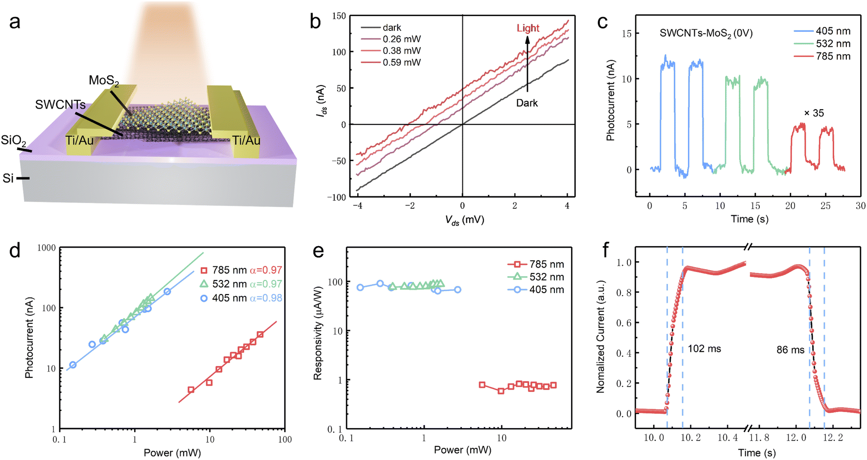 | ||
| Fig. 2 Optoelectronic performance of the SWCNT–MoS2 PTE photodetector. (a) Schematic diagram of the device based on SWCNT–MoS2 hybrid films. (b) Ids–Vds characteristic curves of the detector under darkness and light illumination. (c) Photoresponse of the device under different wavelength lasers with an identical power of 0.15 mW. (d) Power-dependent photocurrent and (e) photoresponsivity of the device under 405, 532, and 785 nm light illumination. (f) The response speed of the device under 532 nm light illumination. | ||
Two key metrics for the photodetector, photoresponsivity (R) and detectivity (D*), were evaluated. They can be defined by the formulas:
| R = Iph/Pin | (2) |
| D* = RS1/2/(2qId)1/2 | (3) |
To better understand the origin of photogeneration in SWCNT–MoS2 heterostructures, we performed scanning photocurrent microscopy (SPCM) measurements at room temperature to probe the spatial distribution of the photocurrent. The left panel in Fig. 3a shows the optical image of the sample for SPCM measurements. The Raman mapping images collected from the channel area clearly reveal the intact triangular MoS2 monolayers and non-uniform distribution of SWCNTs (right panels, Fig. 3a). When the laser spot focuses on the different sides of the heterojunction, opposite photocurrent signals appear, and the shape of the SPCM map can be well maintained with the increase of laser power from 0.29 to 0.72 mW (Fig. 3b and ESI Fig. S14†). The profiles of current intensity along the channel are plotted in Fig. 3c. With the rise of the laser power, one can see that the photocurrent gradually increases in each heterogeneous region without any deviation. The current extracted from the peak position linearly increases from 3.7 to 10.8 nA, and the reverse current at the opposite side also linearly changes from 2.2 to 5.7 nA (Fig. 3d). The results imply that the PTE effect plays a critical role in the photogeneration in SWCNT–MoS2 devices.13,28–30
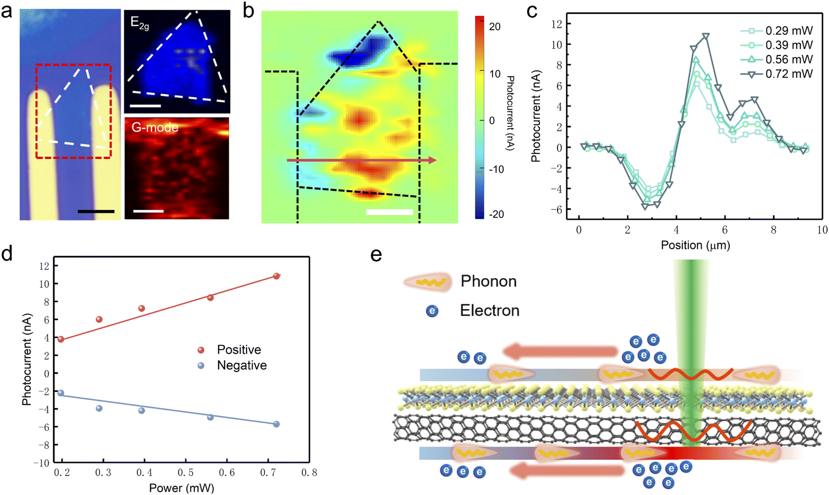 | ||
| Fig. 3 Local laser-induced thermoelectric current mapping. (a) Optical image of the photodetector based on SWCNT–MoS2 hybrid films, which are marked by dashed lines with different colours. Scale bar: 5 μm. Raman mapping of MoS2 and SWCNT in the red rectangle region (right). Scale bar: 2 μm. (b) Spatial distribution of photocurrent induced by 532 nm laser illumination. Scale bar: 2 μm. (c) The current intensity profile of the same line cut along the centre of the channel. (d) Power-dependence of positive and negative currents. (e) Laser excitation induced temperature and carrier distribution in SWCNT–MoS2 heterostructures. | ||
As shown in Fig. 3e, for the photodetector operating in the PTE model, hot carriers are generated under local laser irradiation, followed by scattering with optical phonons, which would result in the localized temperature rise of SWCNT–MoS2 hybrid films. The temperature gradient would cause a voltage difference between hot and cold regions, thus leading to the photocurrent generation. Therefore, a large photocurrent can be expected with a steep temperature gradient between two electrodes. The opposite photogeneration can be attributed to the inversion of the temperature gradient at different positions.13,31 We observed a good linear Ids–Vds characteristic and large Voc variances in the SWCNT–MoS2 PET photodetector. This is in sharp contrast to the photovoltaic photodetector, which works relying on the built-in electric field via the Schottky contact or p–n junction and usually exhibits asymmetric Ids–Vds characteristics.32–35
Compared to the device based on pure SWCNT films, the active area for photogeneration extends considerably to the middle region of the channel in the SWCNT–MoS2 PTE photodetector (ESI Fig. S15†), which indicates that a half thermal diffusion length is enough to generate a distinct photocurrent. It can be well explained by the high temperature rise in the illumination area and the low thermal conductivity of SWCNT–MoS2 hybrid films. On one hand, light absorption in the visible band is significantly enhanced by integrating MoS2 monolayers into SWCNT films (ESI Fig. S11†). Excited electron–hole pairs in MoS2 monolayers would relax to the edge of energy bands before recombination, and the facilitated photo-thermal conversion would result in an effective temperature rise after light illumination.36 On the other hand, a mass concentration of defects, including S vacancies in MoS2, lattice distortion at the heterointerface, and nanopores in SWCNT networks, exist in SWCNT–MoS2 hybrid films. Therefore, a strong phonon scattering effect and inhibited heat flow along the channel can be expected.37–39 As a result, a pronounced PTE effect is demonstrated in the photodetector based on SWCNTs–MoS2 hybrid films.
The polarization sensitivity provides an additional dimension of information for developing new applications of photodetectors such as polarized light imaging40 and photoswitching.41 Benefitting from the anisotropic optical absorption in SWCNT–MoS2 hybrid films, the PTE photodetector also demonstrates polarization-dependent photocurrent generation. As shown in Fig. 4a, linearly polarized light is obtained by introducing a polarizer into the optical system, and the polarization angle can be modulated with a half-wave plate rotating from 0° (parallel to the channel) to 360°. The polarization-resolved absorption spectra of SWCNTs–MoS2 hybrid films are given in Fig. 4b. The inset of Fig. 4b provides the OM image of the sample for measurements. We can see that the maximum light absorbance is obtained with the incident light parallel to the axial direction of the strips, and the minimum value is achieved along the perpendicular direction. The polarization-dependent optical absorbance of the hybrid films was plotted into polar coordinates for clarity (ESI Fig. S16†), which can be fitted using the function:
Iabs = acos![[thin space (1/6-em)]](https://www.rsc.org/images/entities/char_2009.gif) 2θ + bsin2θ 2θ + bsin2θ | (4) |
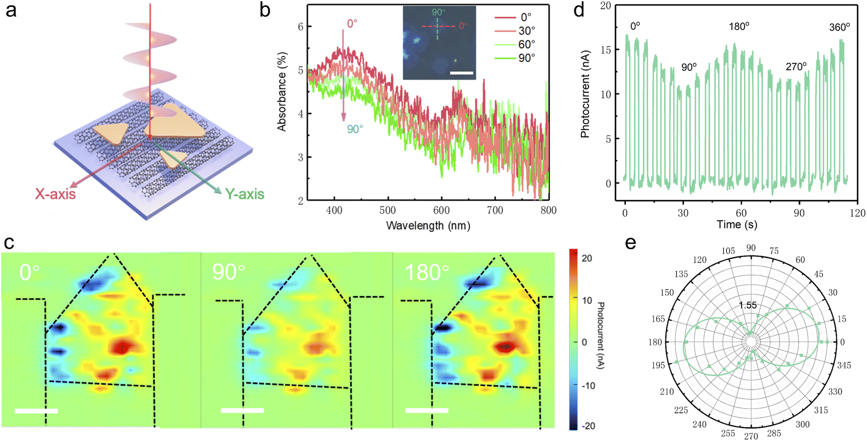 | ||
| Fig. 4 Polarization-resolved photodetector based on SWCNT–MoS2 heterostructures. (a) Schematic diagram of the polarization-dependent absorption measurement. (b) Polarization-sensitive absorption spectrum of SWCNT–MoS2 hybrid films. Scale bar: 10 μm. (c) Spatial distribution of photocurrent under excitation by 0°, 90°, and 180° linearly polarized 532 nm lasers. Scale bar: 2 μm. (d) Linear polarized light dependence of photocurrent under 532 nm illumination. (e) Polar coordinates of the polarization-sensitive photoresponse under 532 nm laser illumination. | ||
Fig. 4c presents the polarization-resolved photocurrent mapping images under 532 nm linear polarized light illumination. The photocurrent of the device would decrease gradually with the polarization angle switching from 0° to 90°, and it would rise back to the original value at a polarization angle of 180°. These results are consistent with the polarization-resolved absorption spectra. The detailed polarization-dependent photocurrent of the SWCNT–MoS2 hybrid device under 532 nm laser illumination is plotted in Fig. 4d. The photocurrent fluctuates periodically with the variation of the polarization angle from 0° to 360° and a maximum value of 16.7 nA is achieved at 0° and 180°. The data were then extracted and fitted using the same function (4). As shown in Fig. 4e, the plotted polar figure exhibits a symmetric pattern with two petals. The anisotropy ratio, defined as the ratio between the maximum and minimum value of photocurrent, is calculated to be 1.55 under 532 nm illumination. In addition, 405 and 785 nm linearly polarized lasers are also utilized to investigate the wavelength-dependent polarization response of the device, and anisotropy ratios of 1.36 and 1.55 were obtained, respectively (ESI Fig. S17†). Compared with state-of-the-art PTE photodetectors, the device based on SWCNT–MoS2 hybrid films demonstrates outstanding photoresponsivity and sensitivity to polarized light in the visible band, indicating its great potential for polarized light detection and polarization imaging without an external power source (ESI Table S1†).
Conclusions
In summary, we demonstrated the growth of MoS2 monolayers on aligned SWCNT films through a simple CVD method. The hybrid films reveal an enhanced PTE effect and can work as the channel material for the fabrication of self-powered photodetectors. Under 532 nm illumination, the responsivity of the PTE photodetector based on SWCNT–MoS2 hybrid films increases by 6 times compared with that of the SWCNT counterpart. In addition, the device exhibits a polarization-dependent photocurrent with a maximum anisotropy ratio of 1.55. This work suggests that the combination of 2D materials with 1D materials has great potential for developing high-performance, polarization-sensitive optoelectronic devices.Author contributions
J. K. Q. and P. Y. H. conceived the idea. P. Y. H., H. J. C. and J. K. Q. performed and supervised the growth experiments. P. Y. H., J. K. Q. and L. Z. performed device fabrication and analysed the experimental data. J. K. Q., P. Y. H. and C. Y. X. cowrote the manuscript.Conflicts of interest
Here are no conflicts to declare.Acknowledgements
This work was supported by the National Natural Science Foundation of China (No. 52102161), Natural Science Foundation of Guangdong Province (No. 2021A1515012423), and Shenzhen Science and Technology Program (No. GXWD20201230155427003-20200805161204001, RCBS20200714114911270, RCJC20210706091950025 and KQTD20200820113045083).Notes and references
- J. Lai, Y. Liu, J. Ma, X. Zhuo, Y. Peng, W. Lu, Z. Liu, J. Chen and D. Sun, ACS Nano, 2018, 12, 4055–4061 CrossRef PubMed.
- W. Wu, Y. Wang, Y. Niu, P. Wang, M. Chen, J. Sun, N. Wang, D. Wu and Z. Zhao, ACS Appl. Mater. Interfaces, 2020, 12, 14165–14173 CrossRef PubMed.
- G. Li, H. Zhang, Y. Li, S. Yin, X. Kan, W. Wei, H. Du, B. Ge, C. An, M. Tian, F. Yan, S. Yang, T. Zhai and L. Li, Nano Res., 2022, 15, 5469–5475 CrossRef.
- X. Lu, L. Sun, P. Jiang and X. Bao, Adv. Mater., 2019, 31, e1902044 CrossRef PubMed.
- M. W. Shabbir and M. N. Leuenberger, ACS Nano, 2022, 16, 5529–5536 CrossRef CAS PubMed.
- S. Wu, L. Wang, Y. Lai, W. Y. Shan, G. Aivazian, X. Zhang, T. Taniguchi, K. Watanabe, D. Xiao, C. Dean, J. Hone, Z. Li and X. Xu, Sci. Adv., 2016, 2, e1600002 CrossRef PubMed.
- D. J. Groenendijk, M. Buscema, G. A. Steele, S. Michaelis de Vasconcellos, R. Bratschitsch, H. S. van der Zant and A. Castellanos-Gomez, Nano Lett., 2014, 14, 5846–5852 CrossRef CAS PubMed.
- W. Guo, Z. Dong, Y. Xu, C. Liu, D. Wei, L. Zhang, X. Shi, C. Guo, H. Xu, G. Chen, L. Wang, K. Zhang, X. Chen and W. Lu, Adv. Sci., 2020, 7, 1902699 CrossRef CAS PubMed.
- B. C. St-Antoine, D. Ménard and R. Martel, Nano Res., 2011, 5, 73–81 CrossRef.
- P. Avouris, M. Freitag and V. Perebeinos, Nat. Photonics, 2008, 2, 341–350 CrossRef CAS.
- T. Dürkop, S. A. Getty, E. Cobas and M. S. Fuhrer, Nano Lett., 2003, 4, 35–39 CrossRef.
- Y. Nakai, K. Honda, K. Yanagi, H. Kataura, T. Kato, T. Yamamoto and Y. Maniwa, Appl. Phys. Express, 2014, 7, 025103 CrossRef CAS.
- B. C. St-Antoine, D. Menard and R. Martel, Nano Lett., 2009, 9, 3503–3508 CrossRef CAS.
- C. Liu, H. Hong, Q. Wang, P. Liu, Y. Zuo, J. Liang, Y. Cheng, X. Zhou, J. Wang, Y. Zhao, J. Xiong, B. Xiang, J. Zhang and K. Liu, Nanoscale, 2019, 11, 17195–17200 RSC.
- W. Su, L. Jin, D. Huo and L. Yang, Opt. Quantum Electron., 2017, 49, 197 CrossRef.
- L. Li, Y. Guo, Y. Sun, L. Yang, L. Qin, S. Guan, J. Wang, X. Qiu, H. Li, Y. Shang and Y. Fang, Adv. Mater., 2018, 30, e1706215 CrossRef PubMed.
- P. Y. Huang, J. K. Qin, C. Y. Zhu, L. Zhen and C. Y. Xu, J. Phys.: Condens. Matter, 2021, 33, 493001 CrossRef CAS.
- J.-K. Qin, C. Wang, L. Zhen, L.-J. Li, C.-Y. Xu and Y. Chai, Prog. Mater. Sci., 2021, 122, 100856 CrossRef CAS.
- M. Engel, J. P. Small, M. Steiner, M. Freitag, A. A. Green, M. C. Hersam and P. Avouris, ACS Nano, 2008, 2, 2445–2452 CrossRef CAS PubMed.
- J. Zou, B. Gao, X. Zhang, L. Tang, S. Feng, H. Jin, B. Liu and H. M. Cheng, Acta Phys.-Chim. Sin., 2020, 2008037 Search PubMed.
- Y. H. Lee, X. Q. Zhang, W. Zhang, M. T. Chang, C. T. Lin, K. D. Chang, Y. C. Yu, J. T. Wang, C. S. Chang, L. J. Li and T. W. Lin, Adv. Mater., 2012, 24, 2320–2325 CrossRef CAS PubMed.
- A. M. Dadgar, D. Scullion, K. Kang, D. Esposito, E. H. Yang, I. P. Herman, M. A. Pimenta, E. J. G. Santos and A. N. Pasupathy, Chem. Mater., 2018, 30, 5148–5155 CrossRef CAS.
- H. K. Ng, D. Xiang, A. Suwardi, G. Hu, K. Yang, Y. Zhao, T. Liu, Z. Cao, H. Liu, S. Li, J. Cao, Q. Zhu, Z. Dong, C. K. I. Tan, D. Chi, C.-W. Qiu, K. Hippalgaonkar, G. Eda, M. Yang and J. Wu, Nat. Electron., 2022, 5, 489–496 CrossRef CAS.
- A. M. Rao, P. C. Eklund, S. Bandow, A. Thess and R. E. Smalley, Nature, 1997, 388, 257–259 CrossRef CAS.
- J. Park and Y. G. Jeong, ACS Appl. Electron. Mater., 2022, 4, 386–393 CrossRef CAS.
- M. Zhang and J. T. W. Yeow, ACS Appl. Mater. Interfaces, 2018, 10, 26604–26609 CrossRef CAS.
- P. Stokes, L. Liu, J. Zou, L. Zhai, Q. Huo and S. I. Khondaker, Appl. Phys. Lett., 2009, 94, 042110 CrossRef.
- S. Xu, H. Zobeiri, N. Hunter, H. Zhang, G. Eres and X. Wang, Nano Energy, 2021, 86, 106054 CrossRef CAS.
- K. J. Erikson, X. He, A. A. Talin, B. Mills, R. H. Hauge, T. Iguchi, N. Fujimura, Y. Kawano, J. Kono and F. Leonard, ACS Nano, 2015, 9, 11618–11627 CrossRef CAS PubMed.
- B. C. St-Antoine, D. Menard and R. Martel, Nano Lett., 2011, 11, 609–613 CrossRef CAS PubMed.
- S. Nanot, A. W. Cummings, C. L. Pint, A. Ikeuchi, T. Akiho, K. Sueoka, R. H. Hauge, F. Leonard and J. Kono, Sci. Rep., 2013, 3, 1335 CrossRef.
- B. Zhao, F. Wang, H. Chen, L. Zheng, L. Su, D. Zhao and X. Fang, Adv. Funct. Mater., 2017, 27, 1700264 CrossRef.
- X. Xu, J. Chen, S. Cai, Z. Long, Y. Zhang, L. Su, S. He, C. Tang, P. Liu, H. Peng and X. Fang, Adv. Mater., 2018, 30, e1803165 CrossRef.
- Z. Zhang, Y. Ning and X. Fang, J. Mater. Chem. C, 2019, 7, 223–229 RSC.
- W. Song, J. Chen, Z. Li and X. Fang, Adv. Mater., 2021, 33, e2101059 CrossRef PubMed.
- X. Zhang, P. Cheng, W. Song, S. Rong, J. Huang, D. Wang, P. Schaaf, G. Zhou, Z. Zhang and J. Liu, Chem. Eng. J., 2022, 446, 137084 CrossRef.
- Z. Chen, H. Lv, Q. Zhang, H. Wang and G. Chen, Carbon Energy, 2021, 4, 115–128 CrossRef.
- S. Vaziri, E. Yalon, M. Munoz Rojo, S. V. Suryavanshi, H. Zhang, C. J. McClellan, C. S. Bailey, K. K. H. Smithe, A. J. Gabourie, V. Chen, S. Deshmukh, L. Bendersky, A. V. Davydov and E. Pop, Sci. Adv., 2019, 5, eaax1325 CrossRef PubMed.
- Q. Jin, S. Jiang, Y. Zhao, D. Wang, J. Qiu, D. M. Tang, J. Tan, D. M. Sun, P. X. Hou, X. Q. Chen, K. Tai, N. Gao, C. Liu, H. M. Cheng and X. Jiang, Nat. Mater., 2019, 18, 62–68 CrossRef PubMed.
- L. Tong, X. Huang, P. Wang, L. Ye, M. Peng, L. An, Q. Sun, Y. Zhang, G. Yang, Z. Li, F. Zhong, F. Wang, Y. Wang, M. Motlag, W. Wu, G. J. Cheng and W. Hu, Nat. Commun., 2020, 11, 2308 CrossRef PubMed.
- L. Zhang, Y. Wu, L. Deng, Y. Zhou, C. Liu and S. Fan, Nano Lett., 2016, 16, 6378–6382 CrossRef PubMed.
Footnote |
| † Electronic supplementary information (ESI) available: Schematic growth diagram of SWCNT–MoS2 heterostructures, SEM, XPS and Raman characterization measurements, and optoelectronic performance and photocurrent distribution measurements. See https://doi.org/10.1039/d2na00609j |
| This journal is © The Royal Society of Chemistry 2022 |