DOI:
10.1039/D2NA00488G
(Paper)
Nanoscale Adv., 2022,
4, 3824-3831
Fabrication of a 100 × 100 mm2 nanometer-thick graphite pellicle for extreme ultraviolet lithography by a peel-off and camphor-supported transfer approach†
Received
27th July 2022
, Accepted 5th August 2022
First published on 9th August 2022
Abstract
An extreme ultraviolet (EUV) lithography pellicle is used to physically protect a mask from contaminants during the EUV exposure process and needs to have a high EUV transmittance. The EUV pellicle should be fabricated using a freestanding thin film with several tens of nanometer thickness in an area of 110 × 142 mm2, which is a challenging task. Here, we propose a peel-off approach to directly detach the nanometer-thick graphite film (NGF)/Ni film from SiO2/Si wafer and significantly shorten the etching time of the Ni film. Combined with the residue-damage-free transfer method that used camphor as a supporting layer, we successfully fabricated a large-area (100 × 100 mm2) NGF pellicle with a thickness of ∼20 nm, and an EUV transmittance of ∼87.2%.
1 Introduction
Since the introduction of a pellicle in 1978, the semiconductor industry has used it to protect masks from contaminants, such as particles during lithography patterning.1 With increasing semiconductor integration, lithography has been focused on employing shorter wavelengths, and extreme ultraviolet lithography (EUVL) with a wavelength of 13.5 nm has become the latest technology for realizing sub-7 nm nanodevices. Owing to the nature of EUV light, which is strongly absorbed by virtually all materials, pellicles for deep ultraviolet (DUV) lithography with a wavelength of 193 nm can no longer be used in EUVL. Thus, the development of EUV pellicles for stable mass production is urgently required.2–5 An EUV pellicle consists of a thin film with a structure suspended from a frame with an internal size of 110 × 142 mm2 (ref. 3 and 4) and must meet strict requirements for practical application in EUVL mass production: it should have high EUV transmittance (>90%), excellent thermal conductivity, low reflectance (<0.04%), and chemical stability during exposure to EUV radiation (with a high energy density of >5 W cm−2 in a hydrogen environment). As the EUV source power increases, one of the most important pellicle requirements is heat resistance. Conventional pellicle candidates, such as Si,4,5 SiNx,6 and Si–Mo–Nb multilayers,4 will be damaged by the high temperature caused by EUV radiation owing to their low thermal conductivity and emissivity. Therefore, carbon-based materials such as carbon nanotubes7 and nanometer-thick graphite films (NGFs),8 which possess excellent thermal conductivity, have been studied as pellicle candidates. Several methods for synthesizing NGFs by chemical vapor deposition (CVD) have been reported previously.8–11 Furthermore, the feasibility of the NGF pellicle for EUVL was demonstrated by fabricating and evaluating a freestanding NGF.12 The most well-known method for fabricating a freestanding NGF is using polymethyl methacrylate (PMMA) as a supporting layer.12–17 However, the transfer method using PMMA leaves residues on a large area even after its removal. In addition, due to the high surface tension of acetone, removing PMMA with acetone causes damage in freestanding samples larger than 10 × 10 mm2. Therefore, for large freestanding samples exceeding 50 × 50 mm2, PMMA cannot be removed with acetone and O2 plasma treatment is required. However, the method of removing PMMA with O2 plasma treatment still leaves PMMA residues on the NGF surface and also causes additional defects and deflection in the free-standing NGF.18 The way to solve various problems caused by using PMMA as a supporting layer is to use sublimable substances such as anthracene,19,20 naphthalene,21 and camphor.22–24 In our previous work, a 30 × 30 mm2 freestanding NGF (thickness ∼ 20 nm) pellicle was fabricated by using camphor as a supporting layer instead of PMMA.18 However, as the sample size increases, the thickness of camphor deposited on the NGF/Ni film/SiO2/Si wafer also needs to increase, which will greatly prolong the etching time of the Ni film. As the etching time increases, the NGF will gradually separate from the camphor and cause the freestanding process to fail. In this study, we developed a process to peel NGF/Ni films directly from SiO2/Si wafers, which can greatly reduce the thickness of the camphor to be deposited and the etching time of Ni films, thus shortening the processing time, and finally proving that a residue-free and high-EUV-transmittance NGF pellicle with an area of 100 × 100 mm2 can be fabricated.
2 Experimental section
2.1. Synthesis of a nanometer-thick graphite film
To fabricate a large-area NGF pellicle of 100 × 100 mm2, we sputtered 1.5 μm Ni films on 8 inch SiO2/Si wafers and used them as the catalyst substrates for NGF growth (base pressure: 5 × 10⁻⁶ torr, sputtering power: 100 W, Ar flow rate: 100 sccm, working pressure: 12 mTorr). The NGF was synthesized using a cold-wall CVD system designed for fabricating large-area samples. The Ni film/SiO2/Si wafer was first loaded into the CVD system and the chamber was heated to 900 °C within 20 min with flowing 15 sccm H2 gas (0.04 torr). Then, 100 sccm CH4 gas (0.34 torr) was introduced into the chamber and the temperature was maintained at 900 °C for 10 min. After 10 min, the chamber was cooled from 900 °C to 700 °C (cooling rate ∼ 3 °C s−1) to form the NGF. Then the chamber was naturally cooled to room temperature within 25 min (from 700 to 400 °C (cooling rate ∼ 1.5 °C s−1), 400 to 200 °C (∼0.6 °C s−1), 200 to 25 °C (∼0.25 °C s−1)).
2.2. Freestanding process to fabricate a NGF pellicle
To fabricate a NGF synthesized on a Ni film (1.5 μm)/SiO2/Si wafer substrate as a pellicle, a process of transferring the NGF to the desired frame is required. The process is illustrated in Fig. 1. The first step is peeling off the NGF/Ni film from the SiO2/Si wafer (Fig. 1(b)). A temporary transfer film (TTF) was produced by attaching a polyethylene terephthalate (PET) film with a square hole in the middle on top of the NGF/Ni film. And then, an additional cover film (PET) was attached onto the TTF to prevent excessive deformation of the TTF during the peeling process. Then, the TTF attached NGF/Ni film/SiO2/Si wafer was slowly peeled in distilled (DI) water, which allowed the Ni film to be delaminated from the SiO2/Si wafer. At the time, water penetrates between Ni and SiO2, generating the effect of water-assisted subcritical debonding and allowing easy separation between Ni and SiO2.25–27 Then, by attaching a supporting frame on the peeled TTF, a NGF/Ni film in freestanding form was produced, as shown in Fig. 1(c). Then, the freestanding NGF/Ni film was loaded into the camphor deposition chamber. The camphor source was heated to 80 °C at a working pressure of 2 torr, and the deposition time was 2 min 30 s to form a 160 μm-thick camphor film on the freestanding NGF/Ni film to protect the NGF during the Ni film etching and cleaning process (Fig. 1(d)). The 1.5 μm Ni film was removed from the camphor/NGF/Ni film by dipping the sample in ferric chloride (FeCl3) solution for 10 min. Then, the freestanding camphor/NGF was transferred to DI water and rinsed for 10 min twice (Fig. 1(e)). The camphor/NGF sample was later transferred onto an adhesive-coated frame with a freestanding structure, and the camphor was sublimated in a chamber with an ethanol vapor atmosphere obtained by heating ethanol to 75 °C (Fig. 1(f)). After 48 h, the camphor was completely sublimated from the NGF surface, and the supporting frame was removed. Finally, the 100 × 100 mm2 NGF pellicle was thus fabricated (Fig. 1(g)) (see more freestanding process details in Fig. 3).
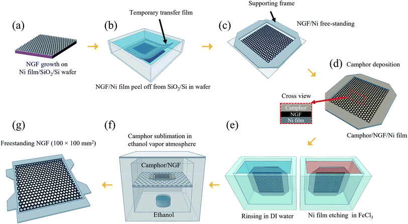 |
| | Fig. 1 Schematic of the NGF pellicle fabrication process. (a) NGF/Ni film/SiO2/Si; (b) NGF/Ni film is peeled off from the SiO2/Si wafer in DI water; (c) the supporting frame is attached; (d) after camphor deposition on a freestanding NGF/Ni film. The inset shows a cross-sectional illustration. (e) Ni film etching in FeCl3 solution and rinsing in DI water. (f) Camphor removal process in an ethanol vapor atmosphere. (g) Freestanding NGF sample (100 × 100 mm2) after camphor removal. | |
2.3. Characterization
The NGF thickness was measured using an atomic force microscope (AFM) (ParkNX10, Park Systems Corp.) after transferring the NGF onto SiO2/Si. The thickness (cross-section) and the surface of the camphor deposited on NGF/Ni/SiO2/Si were evaluated by optical microscopy (Olympus BX51M). Raman mapping (100 × 100 μm2, alpha300 M, WITec, 532 nm laser excitation) was performed to compare the crystallinity of raw and freestanding NGFs fabricated using the transfer method. Cross-sectional samples of NGF/Ni were prepared using the focused ion beam (FIB) (JIB-4601F, JEOL Ltd., Tokyo, Japan) technique, and the NGF/Ni cross-section view was observed using a transmission electron microscope (TEM) (JEM-2100F, JEOL Ltd., Tokyo, Japan) to check the thickness uniformity of the NGF. EUV transmittance of the freestanding NGF (inner diameter 10 mm, and square size 40 × 40 mm2) was measured using an instrument from Samsung Electronics Co. Ltd.
3 Results and discussion
3.1. NGF/Ni film peel-off process from SiO2/Si wafer
In our previous study, freestanding NGF samples with a size of 30 × 30 mm2 were fabricated. The method involved the direct deposition of camphor on the NGF/Ni film/SiO2/Si wafer and the etching of the Ni film. However, this method required 4 h of Ni film etching time to produce 30 × 30 mm2 freestanding samples, and this etching time extended to over 90 h as the size increased to 100 × 100 mm2 (Fig. S1†). In addition, the sublimation of camphor during such a long etching process must be considered, which requires a deposited camphor film with a thickness of more than 500 μm (Fig. S2(a)†). The thicker camphor film results in weaker adhesive force between the camphor and NGF, which makes the NGF easily separate from the camphor as the Ni film etching time increased. Thus, the separation of the camphor and NGF occurred more frequently as the sample size increased. Therefore, the etching time of the Ni film should be significantly shortened.
Meanwhile, processes for transferring a nano-thick film from the catalyst substrate to a target substrate without damage have been extensively studied. Notably, methods for minimizing damage involve reducing the interfacial adhesion energy (Gc) between the catalyst substrate and the nano-thick film by transferring in a liquid such as water.28,29 The Ni film and SiO2/Si wafer can be separated in water using a thermal-release tape and then transferred to a target substrate.27,30–32 However, considering that this method used a thermal-release tape attached to the thin film, the residue cannot be entirely removed from the thin film surface after the removal of the tape by applying heat. In addition, such a transfer method cannot be used to fabricate a pellicle with a freestanding structure because it cannot be transferred onto a frame with an empty middle. Therefore, we developed a process for separating the pure NGF/Ni film from SiO2/Si wafer without coating a sacrificial layer or attaching a thermal-release tape on the NGF/Ni film. To peel off the NGF/Ni film, the TTF with a square hole (110 × 110 mm2) was first attached in the middle of the NGF/Ni film (Fig. 2a and b(i)). This open square would subsequently contain the freestanding NGF. A cover film was attached to prevent contact between the NGF and water and the distortion of the TTF during peel-off process that was performed in water (Fig. 2b(i)). As shown in Fig. 2a and b(ii), the sample was fixed on the bottom of a water bath and peeled off slowly with a speed of 2 mm s−1 or less to minimize the stress applied to the Ni film.32 Due to the water-assisted subcritical debonding, the interface between Ni and SiO2 can be easily separated, which resulted in the peel-off of the TTF with the NGF/Ni film from the initial Si/SiO2 wafer (Fig. 2b(ii)).25–27 The cover film was subsequently removed, and a supporting frame was attached to the TTF to facilitate the camphor deposition and Ni film etching process (cross-sectional structure in Fig. S3†). As shown in Fig. 2a(iii), the empty square area within the supporting frame is in a state of a freestanding NGF/Ni film and turned into a pellicle after all transfer processes were finished. Fig. S4(a)† shows an optical image of the surface of the freestanding NGF/Ni film.
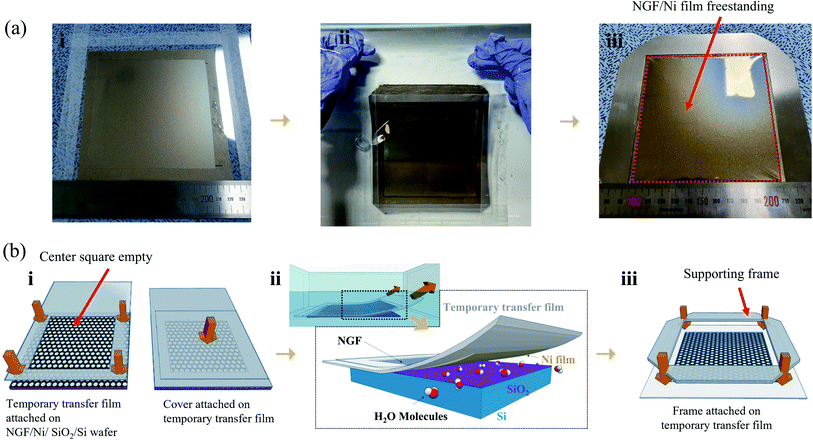 |
| | Fig. 2 (a) Photographs of the NGF/Ni film peel off process. (b) Schematic of the NGF/Ni film peel off process in (a) and the mechanism. (i) Temporary transfer film (TTF) attachment on the NGF/Ni film/SiO2/Si wafer. (ii) NGF/Ni film peel off from SiO2/Si wafer in DI water. (iii) Removal of the cover on the peeled temporary transfer film (NGF/Ni film) and attachment of the support frame. | |
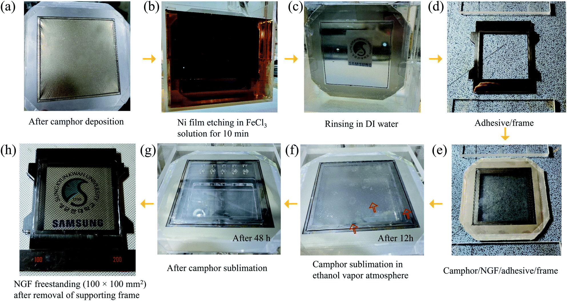
3.2. Camphor deposition and sublimation process
In addition to its low adhesion to graphene, camphor has lower adsorption energy (0.09 eV per camphor molecule23) than polymers such as SPPOI,33 rosin,34 pentacene,35 and PMMA.36 Consequently, it sublimates easily over time without leaving any residue on the NGF surface even at room temperature and atmospheric pressure. Additionally, given its ability to be formed into a rigid film with a thickness of several hundred micrometers or more, camphor can be used as a supporting layer by replacing PMMA in the freestanding process. In our previous study, we replaced PMMA with camphor to overcome problems encountered during transfer, such as residues, defects, and deflections. Consequently, a freestanding NGF with an inner size of 30 × 30 mm2 was fabricated.18 In conclusion, camphor is suitable for use as a supporting layer to fabricate a large-area NGF pellicle with an internal size of 100 × 100 mm2. Fig. 3(a) is a photograph of camphor deposited on a freestanding NGF/Ni film. The deposited camphor had a thickness of 160 μm (Fig. S2(b)†) and was used as a supporting layer for the transfer process (Fig. S4(b)† shows an optical image of the camphor/NGF/Ni film surface). The Ni film was etched by vertically dipping the freestanding camphor/NGF/Ni film stack in FeCl3 solution (Fig. 3(b)). Then, the freestanding camphor/NGF was dipped in DI water and rinsed twice for 10 min (Fig. 3(c)). As shown in Fig. 3(e), camphor/NGF was placed on the adhesive-coated frame (Fig. 3(d)) and camphor was sublimated in a chamber in an ethanol vapor atmosphere. After 12 h, camphor was released from the right end (Fig. 3(f)); after 48 h, all of the camphor sublimated (Fig. 3(g)). Finally, after the removal of the supporting frame, an NGF pellicle with a thickness of ∼20 nm and an inner size of 100 × 100 mm2 was obtained (Fig. 3(h)). Fig. S4(c)† shows an optical image of the surface of the freestanding NGF.
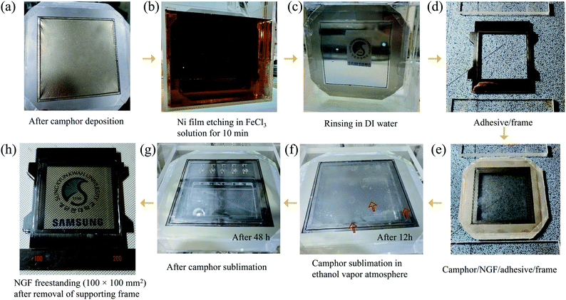 |
| | Fig. 3 Photographs of the NGF pellicle fabrication process. (a) After camphor deposition on the NGF/Ni film. (b) Ni film etching in FeCl3 solution for 10 min. (c) Camphor/NGF rinsing in DI water. (d) Freestanding frame application using an adhesive. (e) Stamping of camphor/NGF on a frame with an adhesive applied. (f) After 12 h of camphor sublimation in an ethanol vapor atmosphere chamber. (g) Freestanding NGF after all camphor was removed after 48 h. (h) 100 × 100 mm2 freestanding NGF after removal of the supporting frame. | |
3.3. Comparison of NGF characteristics before and after the transfer process
To transfer a thin film onto a substrate, the most common method is to coat a polymer film such as PMMA to be a supporting layer. However, such materials cannot be completely removed after transfer, leaving residues or defects on the surface of the samples.34,37–40 In contrast, camphor does not affect the thin film even when used as a supporting layer for transferring thin films.22–24
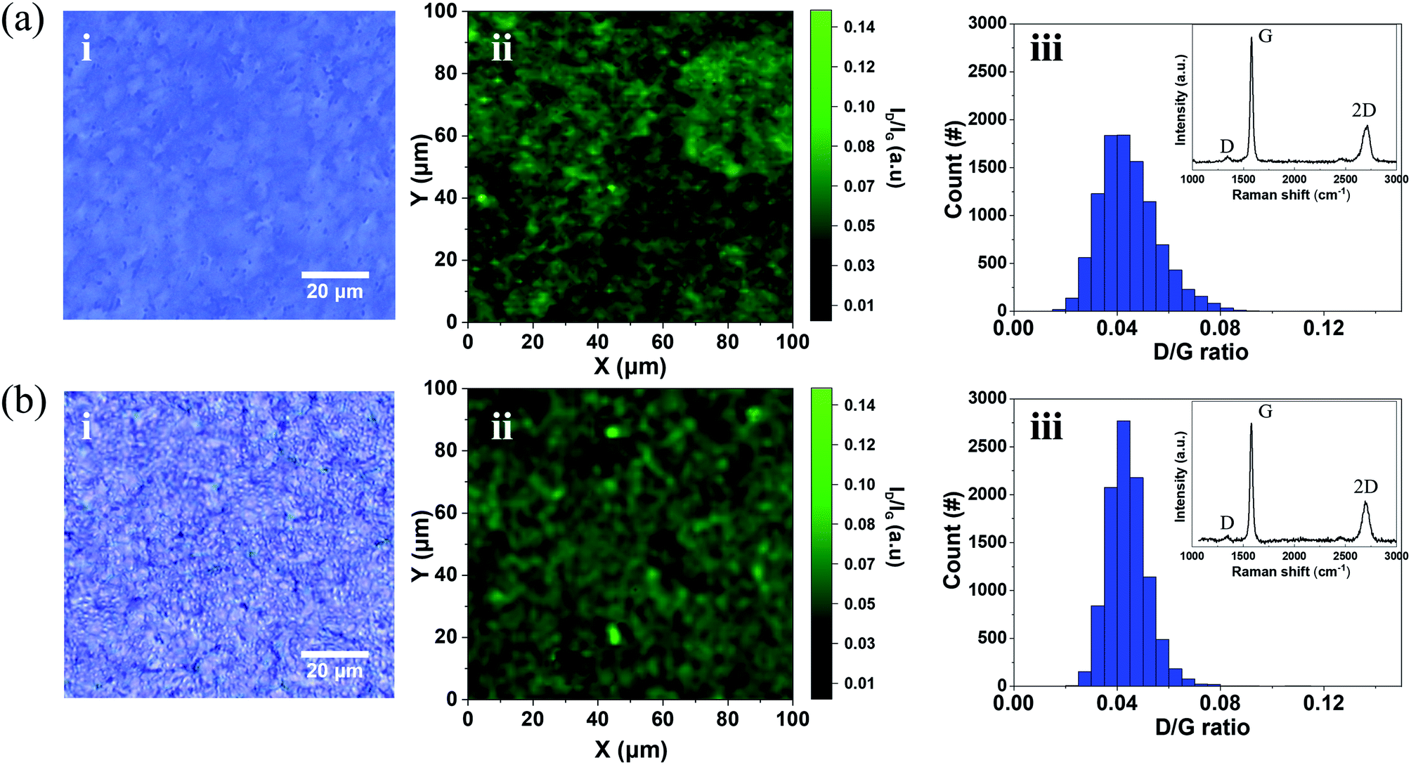
Fig. 4 shows Raman spectrum mapping, which was conducted to precisely evaluate the crystallinity of the NGF and the residues on its surface before and after the camphor-supported transfer. Fig. 4a(i) is an optical image showing the surface of a raw NGF transferred onto a SiO2/Si wafer without using a supporting layer. Fig. 4a(ii) shows the Raman mapping image of the D/G intensity ratio (ID/IG) of (i). Fig. 4(b) is the Raman mapping of the freestanding NGF using camphor as a supporting layer. Fig. 4b(i) shows the surface optical image of the freestanding NGF, and Fig. 4b(ii) shows the ID/IG mapping. Fig. 4a(iii) shows the distribution of ID/IG. The average ID/IG ratio value of the raw NGF is 0.04, and its values range between 0.09 and 0.01. The average ID/IG ratio of the freestanding NGF in Fig. 4b(iii) is also 0.04, and its values range between 0.08 and 0.01, indicating that the raw and freestanding NGFs had unchanged ID/IG ratios and no defects were generated during the camphor transfer process. Additionally, the inset Raman spectrum in Fig. 4b(iii) shows only the graphite-related Raman peaks corresponding to the D (1350 cm−1), G (1595 cm−1), and 2D (2700 cm−1) bands; no typical peak of a camphor like carbon ring (652 cm−1) and C![[double bond, length as m-dash]](https://www.rsc.org/images/entities/char_e001.gif) O stretching vibration (1741 cm−1) appeared.41 Therefore, the camphor-supported transfer does not cause any defects or leave camphor residues on the NGF.
O stretching vibration (1741 cm−1) appeared.41 Therefore, the camphor-supported transfer does not cause any defects or leave camphor residues on the NGF.
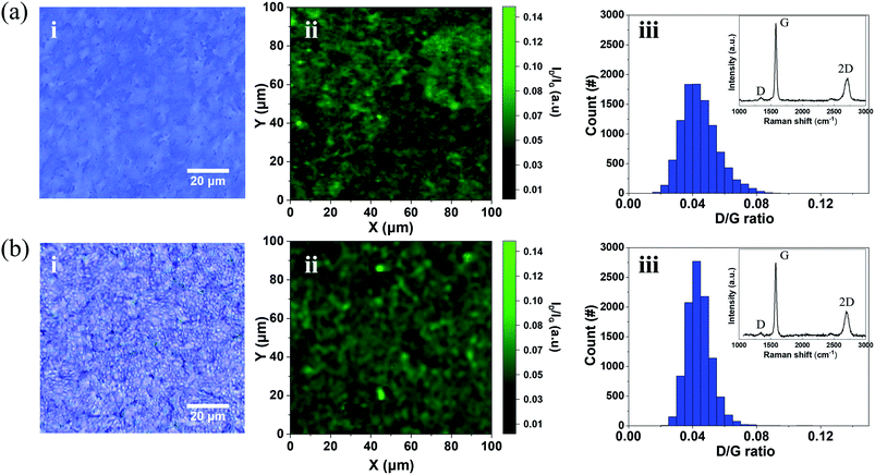 |
| | Fig. 4 Comparison of NGF characteristics before and after the transfer process. Observation of the NGF surface: (a) raw NGF after CVD growth; (b) freestanding NGF after camphor sublimation. (i) The optical image of Raman mapping; (ii) intensity ratio of the D to G band (ID/IG) in the Raman map of the NGF. (iii) Histogram of ID/IG and the inset in (iii) is the Raman spectrum of the NGF. | |
3.4. EUV transmittance of the NGF pellicle
The EUV transmission of a freestanding NGF was measured at a wavelength of around 13.5 nm to confirm the feasibility of the NGF EUV pellicle. The freestanding NGF sample with an inner diameter of 40 mm was prepared. Fig. 5 shows the NGF freestanding photograph fabricated via the peel-off and camphor-supported transfer process described in Fig. 1 and the measured EUV transmittance value. In Fig. 5(a), the freestanding NGF with a size of 40 × 40 mm2 was fabricated using the same NGF as the 100 × 100 mm2 freestanding NGF shown in Fig. 3(h). Fig. 5(b) shows the EUV transmittance mapping (1 mm beam size, 900 points) of the center 30 × 30 mm2 area marked by a red square in the 40 × 40 mm2 freestanding NGF shown in (a); we didn't collect the data near the frame edge boundary to ensure the data accuracy. The average EUV transmittance of the 30 × 30 mm2 freestanding NGF was 87.2%, and the relative standard deviation was 0.78% in (c). EUV transmittance can be converted into the thickness of the NGF using a known formula (TEUV = e−4πβN×d/λ, where β = 6.9054 × 10⁻³ at λ = 13.5 nm and N × d is the thickness of the NGF12,42). The calculation result shows that the thickness of the NGF is 21 nm. Monolayer graphene absorbs 0.2% of EUV (graphene thickness ∼ 0.34 nm). The standard deviation is approximately 0.78%, which can be interpreted to reflect the graphene error in approximately three or four layers. Consequently, the NGF pellicle with a size of 100 × 100 mm2 had a thickness of 21 ± 1.2 nm.
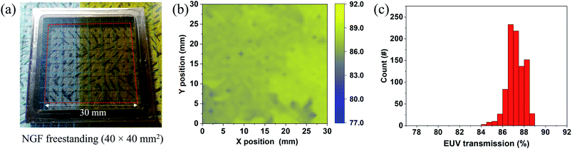 |
| | Fig. 5 Measurement of EUV transmittance of the NGF. (a) Photograph of a freestanding NGF (40 × 40 mm2). (b) EUV transmittance mapping image of a NGF with an area of 30 × 30 mm2 marked by a red square in (a). (c) Histogram of EUV transmission. | |
Due to the reflective mask used in EUVL, EUV light passes through the pellicle twice. If the pellicle does not have high EUV transmittance, EUV photons are absorbed by the pellicle, reducing the number of photons focused on the wafer. For this reason, an EUV transmittance of 90% or more is required for the commercialization of the EUV pellicle. The NGF freestanding sample with an inner diameter of 10 mm was prepared by thinning the thickness of the NGF for more than 90% EUV transmittance (Fig. S5†). The average EUV transmission in the freestanding NGF is 91.6% (relative standard deviation, 0.85%, Fig. S5(c)†), and the thickness was 14 nm as measured by AFM and TEM (see Fig. S6†).
3.5. NGF thickness uniformity
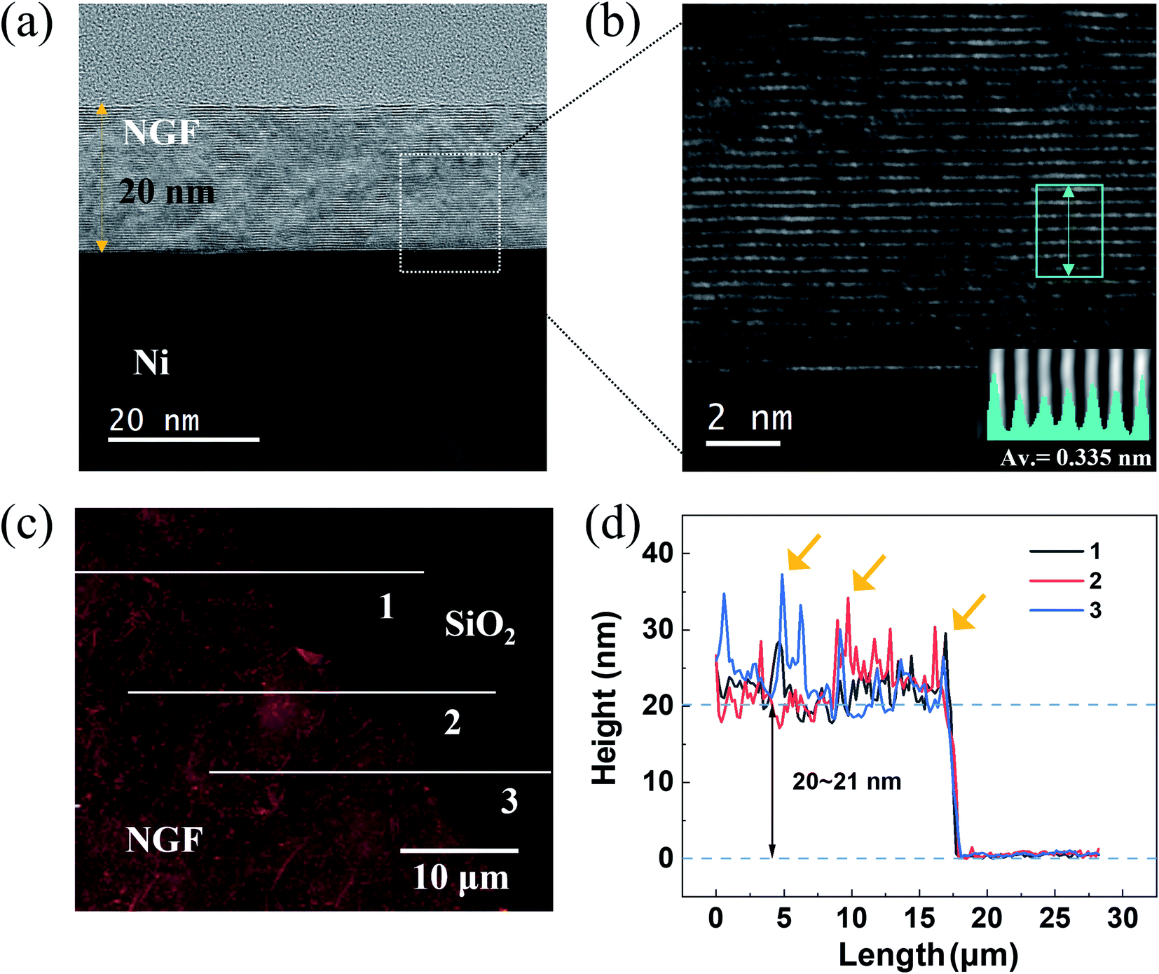
To compare the thickness of the NGF calculated by EUV transmittance with the actual thickness, the thickness of the NGF was confirmed by TEM and AFM. In the TEM cross-sectional view of the NGF/Ni film shown in Fig. 6(a), a NGF with a thickness of 20 nm was uniformly grown. Moreover, the well-ordered, stacked structure with an interlayer spacing of 0.33 to 0.34 nm can be seen in the high-magnification TEM image in Fig. 6(b) and the line-scanning intensity profile inset at the bottom right. Fig. 6(c) shows a typical AFM topographic image, and Fig. 6(d) shows the NGF height profile corresponding to the solid line in Fig. 6(c). The measured average thickness of the NGF is 20–21 nm, and the areas (yellow arrows) with a thickness deviation exceeding 10 nm are small wrinkles formed due to the difference in thermal expansion coefficients between Ni and the NGF.43
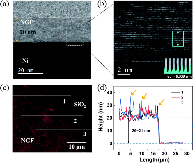 |
| | Fig. 6 NGF thickness analysis and cross-sectional TEM images of the NGF: (a) low magnification and (b) higher magnification TEM images of the NGF marked with a white rectangle in (a) and the line-scanning intensity profile (inset bottom-right) obtained from the area highlighted with a cyan rectangle. (c) AFM image of the NGF on the SiO2/Si wafer. (d) Thickness profile corresponding to the line shown in (c). | |
4 Conclusions
In conclusion, we developed an NGF/Ni film peel-off process and fabricated a large-area NGF pellicle with a size of 100 × 100 mm2via a transfer method using camphor as a supporting layer. By peeling off the NGF/Ni film from the SiO2/Si wafer, the etching time of the Ni film was significantly decreased from 95 h to 10 min. Accordingly, the separation of the NGF from camphor/NGF caused by the long etching time can be overcome. Moreover, the thickness of deposited camphor was reduced by approximately 160 μm from the previous 550 μm, thereby decreasing the processing time required for camphor removal. No difference was observed in the comparison of D/G intensity ratios (ID/IG) before and after the transfer between raw and freestanding NGFs (0.04), indicating that the transfer did not generate any additional defects. Furthermore, EUV transmittance mapping at 13.5 nm yielded 91.6% (10 mm in diameter, thickness ∼ 14 nm) and 87.2% (40 × 40 mm2, thickness ∼ 20 nm). We suggest the peel-off process and the camphor-supported transfer method as solutions to the scale-up of the NGF pellicle, which has been the biggest problem for the commercialization of pellicles for EUVL. In the future, this freestanding method will also be applied to fabricate pellicles by stacking a capping layer on the NGF. Our practical freestanding method is not restricted to pellicle applications but can be applied to various fields requiring freestanding, including EUV spectral purity filters, thin-film sensors, and speaker diaphragms.
Author contributions
K.-B. Nam conceptualized the idea and designed the research. Q. C. Hu synthesized the NGFs. Q. C. Hu and J.-H. Yeo assisted with atomic force microscopy and Raman measurements. M. J. Kim evaluated the optical properties of NGF pellicles. J.-B. Yoo and M. J. Kim devised and supervised the project. All co-authors contributed to the discussions and writing the manuscript.
Conflicts of interest
There are no conflicts to declare.
Acknowledgements
This work was supported by the Samsung Electronics' University R&D Program (IO 201020-07708-01, IO 211018-09023-01).
Notes and references
-
V. Shea and W. Wojcik, US Pat., 1978, 4131363 Search PubMed.
- Y. A. Shroff, M. Goldstein, B. Rice, S. H. Lee, K. Ravi and D. Tanzil, Proc. SPIE, 2006, 6151, 615104 CrossRef.
- C. Wagner and N. Harned, Nat. Photonics, 2010, 4, 24–26 CrossRef CAS.
- L. Scaccabarozzi, D. Smith, P. R. Diago, E. Casimiri, N. Dziomkina and H. Meijer, Proc. SPIE, 2013, 8679, 867904 CrossRef.
- C. Zoldesi, K. Bal, B. Blum, G. Bock, D. Brouns, F. Dhalluin, N. Dziomkina, J. D. Arias Espinoza, J. Hoogh, S. Houweling, M. Jansen, M. Kamali, A. Kempa, R. Kox, R. Kruif, J. Lima, Y. Liu, H. Meijer, H. Meiling, I. Mil, M. Reijnen, L. Scaccabarozzi, D. Smith, B. Verbrugge, L. Winter, X. Xiong and J. Zimmerman, Proc. SPIE, 2014, 9048, 90481N CrossRef.
- D. L. Goldfarb, Proc. SPIE, 2015, 9635, 96350A Search PubMed.
- J. Bekaert, E. Gallagher, R. Jonckheere, L. Van Look, R. Aubert, V. V. Nair, M. Y. Timmermans, I. Pollentier, E. Hendrickx, A. Klein, G. Yegen, P. Broman, N. M. Felix and A. Lio, Proc. SPIE, 2021, 11609, 116090Z Search PubMed.
- Q. Hu, S. G. Kim, D. W. Shin, T. S. Kim, K. B. Nam, M. J. Kim, H. C. Chun and J. B. Yoo, Carbon, 2017, 113, 309–317 CrossRef CAS.
- S. G. Kim, Q. Hu, K. B. Nam, M. J. Kim and J. B. Yoo, Chem. Phys. Lett., 2018, 698, 157–162 CrossRef CAS.
- Q. C. Hu, S. Kim, B. Nam, J. H. Yeo, T. E. S. Kim, M. A. Kim and J. E. O. Yoo, Carbon, 2019, 144, 410–416 CrossRef CAS.
- Q. Hu, K. B. Nam, J. H. Yeo, M. J. Kim and J. B. Yoo, Carbon, 2021, 177, 35–43 CrossRef CAS.
- S. G. Kim, D. W. Shin, T. Kim, S. Kim, J. H. Lee, C. G. Lee, C. W. Yang, S. Lee, S. J. Cho, H. C. Jeon, M. J. Kim, B. G. Kim and J. B. Yoo, Nanoscale, 2015, 7, 14608–14611 RSC.
- Q. Zhou and A. Zettl, Appl. Phys. Lett., 2013, 102, 223109 CrossRef.
- Q. Zhou, J. L. Zheng, S. Onishi, M. F. Crommie and A. K. Zettl, Proc. Natl. Acad. Sci. U. S. A., 2015, 112, 8942–8946 CrossRef CAS PubMed.
- Y. M. Chen, S. M. He, C. H. Huang, C. C. Huang, W. P. Shih, C. L. Chu, J. Kong, J. Li and C. Y. Su, Nanoscale, 2016, 8, 3555–3564 RSC.
- S. A. Akbari, V. Ghafarinia, T. Larsen, M. M. Parmar and L. G. Villanueva, Sci. Rep., 2020, 10, 6426 CrossRef PubMed.
- S. Y. Kim, D. W. Shin, S. G. Kim, K. B. Nam, Q. Hu, T. Kim, Y. H. Gim, H. S. Ko, M. J. Kim and J. B. Yoo, Adv. Mater. Interfaces, 2020, 7, 2001141 CrossRef CAS.
- K. B. Nam, J. H. Yeo, Q. Hu, M. J. Kim, B. Oh and J. B. Yoo, Nanotechnology, 2021, 32, 465301 CrossRef CAS PubMed.
- A. F. Carvalho, A. J. Fernandes, M. B. Hassine, P. Ferreira, E. Fortunato and F. M. Costa, Appl. Mater. Today, 2020, 21, 100879 CrossRef.
- A. Yulaev, G. J. Cheng, A. R. H. Walker, I. V. Vlassiouk, A. Myers, M. S. Leite and A. Kolmakov, RSC Adv., 2016, 6, 83954–83962 RSC.
- M. G. Chen, D. Stekovic, W. X. Li, B. Arkook, R. C. Haddon and E. Bekyarova, Nanotechnology, 2017, 28, 255701 CrossRef PubMed.
- B. Wang, B. V. Cunning, N. Y. Kim, F. Kargar, S. Y. Park, Z. Li, S. R. Joshi, L. Peng, V. Modepalli, X. Chen, Y. Shen, W. K. Seong, Y. Kwon, J. Jang, H. Shi, C. Gao, G. H. Kim, T. J. Shin, K. Kim, J. Y. Kim, A. A. Balandin, Z. Lee and R. S. Ruoff, Adv. Mater., 2019, 31, e1903039 CrossRef PubMed.
- B. N. Chandrashekar, N. D. Cai, L. W. Liu, A. S. Smitha, Z. F. Wu, P. C. Chen, R. Shi, W. J. Wang, J. W. Wang, C. M. Tang and C. Cheng, J. Colloid Interface Sci., 2019, 546, 11–19 CrossRef CAS PubMed.
- B. Wang, D. Luo, Z. Li, Y. Kwon, M. Wang, M. Goo, S. Jin, M. Huang, Y. Shen, H. Shi, F. Ding and R. S. Ruoff, Adv. Mater., 2018, 30, e1800888 CrossRef PubMed.
- S. Y. Kook and R. H. Dauskardt, J. Appl. Phys., 2002, 91, 1293–1303 CrossRef CAS.
- C. H. Lee, D. R. Kim and X. L. Zheng, Nano Lett., 2011, 11, 3435–3439 CrossRef CAS PubMed.
- C. H. Lee, J. H. Kim, C. Zou, I. S. Cho, J. M. Weisse, W. Nemeth, Q. Wang, A. C. van Duin, T. S. Kim and X. Zheng, Sci. Rep., 2013, 3, 2917 CrossRef PubMed.
- Y. Zhang, Q. C. Liu and B. X. Xu, Extreme Mech. Lett., 2017, 16, 33–40 CrossRef.
- Y. Zhang, B. O. O. Kim, Y. Gao, D. S. Wie, C. H. Lee and B. X. Xu, Int. J. Solids Struct., 2019, 180, 30–44 CrossRef.
- C. H. Lee, D. R. Kim, I. S. Cho, N. William, Q. Wang and X. Zheng, Sci. Rep., 2012, 2, 1000 CrossRef PubMed.
- C. H. Lee, D. R. Kim and X. L. Zheng, ACS Nano, 2014, 8, 8746–8756 CrossRef CAS PubMed.
- D. S. Wie, Y. Zhang, M. K. Kim, B. Kim, S. Park, Y. J. Kim, P. P. Irazoqui, X. L. Zheng, B. X. Xu and C. H. Lee, Proc. Natl. Acad. Sci. U. S. A., 2018, 115, E7236–E7244 CrossRef CAS PubMed.
- Y. Y. Han, L. Zhang, X. J. Zhang, K. Q. Ruan, L. S. Cui, Y. M. Wang, L. S. Liao, Z. K. Wang and J. S. Jie, J. Mater. Chem. C, 2014, 2, 201–207 RSC.
- Z. Zhang, J. Du, D. Zhang, H. Sun, L. Yin, L. Ma, J. Chen, D. Ma, H. M. Cheng and W. Ren, Nat. Commun., 2017, 8, 14560 CrossRef CAS PubMed.
- H. H. Kim, B. Kang, J. W. Suk, N. Li, K. S. Kim, R. S. Ruoff, W. H. Lee and K. Cho, ACS Nano, 2015, 9, 4726–4733 CrossRef CAS PubMed.
- Y. C. Lin, C. C. Lu, C. H. Yeh, C. H. Jin, K. Suenaga and P. W. Chiu, Nano Lett., 2012, 12, 414–419 CrossRef CAS PubMed.
- Z. Cheng, Q. Zhou, C. Wang, Q. Li, C. Wang and Y. Fang, Nano Lett., 2011, 11, 767–771 CrossRef CAS PubMed.
- X. L. Liang, B. A. Sperling, I. Calizo, G. J. Cheng, C. A. Hacker, Q. Zhang, Y. Obeng, K. Yan, H. L. Peng, Q. L. Li, X. X. Zhu, H. Yuan, A. R. H. Walker, Z. F. Liu, L. M. Peng and C. A. Richter, ACS Nano, 2011, 5, 9144–9153 CrossRef PubMed.
- J. H. Mun and B. J. Cho, Nano Lett., 2013, 13, 2496–2499 CrossRef CAS PubMed.
- B. Zhuang, S. Li, S. Li and J. Yin, Carbon, 2020, 173, 609 CrossRef.
- S. Sharma, G. Kalita, M. E. Ayhan, K. Wakita, M. Umeno and M. Tanemura, J. Mater. Sci., 2013, 48, 7036–7041 CrossRef CAS.
- B. L. Henke, E. M. Gullikson and J. C. Davis, At. Data Nucl. Data Tables, 1993, 55, 349 CrossRef CAS.
- A. N. Obraztsov, E. A. Obraztsova, A. V. Tyurnina and A. A. Zolotukhin, Carbon, 2007, 45, 2017–2021 CrossRef CAS.
|
| This journal is © The Royal Society of Chemistry 2022 |
Click here to see how this site uses Cookies. View our privacy policy here. 
 Open Access Article
 This Open Access Article is licensed under a Creative Commons Attribution-Non Commercial 3.0 Unported Licence
 *ad
*ad