
 Open Access Article
 This Open Access Article is licensed under a Creative Commons Attribution-Non Commercial 3.0 Unported Licence
Impact of the gate geometry on adiabatic charge pumping in InAs double quantum dots†
Sung Jin
An‡
ab,
Myung-Ho
Bae‡
 c,
Myoung-Jae
Lee
ade,
Man Suk
Song
ab,
Morten H.
Madsen
f,
Jesper
Nygård
f,
Christian
Schönenberger
gh,
Andreas
Baumgartner
gh,
Jungpil
Seo
*bd and
Minkyung
Jung
*ade
c,
Myoung-Jae
Lee
ade,
Man Suk
Song
ab,
Morten H.
Madsen
f,
Jesper
Nygård
f,
Christian
Schönenberger
gh,
Andreas
Baumgartner
gh,
Jungpil
Seo
*bd and
Minkyung
Jung
*ade
aDGIST Research Institute, DGIST, Daegu 42988, Korea. E-mail: minkyung.jung@dgist.ac.kr
bDepartment of Emerging Materials Science, DGIST, Daegu 42988, Korea. E-mail: jseo@dgist.ac.kr
cKorea Research Institute of Standards and Science, Daejeon 34113, Korea
dInstitute of Next Generation Semiconductor Technology (INST), DGIST, Daegu 42988, Korea
eDepartment of Interdisciplinary Engineering, DGIST, Daegu 42988, Korea
fCenter for Quantum Devices, Niels Bohr Institute, University of Copenhagen, 2100 Copenhagen, Denmark
gDepartment of Physics, University of Basel, Klingelbergstrasse 82, CH-4056 Basel, Switzerland
hSwiss Nanoscience Institute (SNI), University of Basel, Klingelbergstrasse 82, CH-4056 Basel, Switzerland
First published on 11th August 2022
Abstract
We compare the adiabatic quantized charge pumping performed in two types of InAs nanowire double quantum dots (DQDs), either with tunnel barriers defined by closely spaced narrow bottom gates, or by well-separated side gates. In the device with an array of bottom gates of 100 nm pitch and 10 μm lengths, the pump current is quantized only up to frequencies of a few MHz due to the strong capacitive coupling between the bottom gates. In contrast, in devices with well-separated side gates with reduced mutual gate capacitances, we find well-defined pump currents up to 30 MHz. Our experiments demonstrate that high frequency quantized charge pumping requires careful optimization of the device geometry, including the typically neglected gate feed lines.
Introduction
Fast and accurate manipulation of individual charge carriers in nanoscale electronic devices is a key technology in research and development, from quantum information processing with quantum dots (QDs)1,2 to modern quantum metrology.3–6 In particular, the controlled transfer of electrons one-by-one provides a fundamental standard for the electrical current based on the quantized electron charge.3 This process is achieved by quantized charge pumping (CP), in which a periodic modulation of one or several external parameters leads to a DC current of one electron per cycle, thus relating the current to the frequency standard.3–6 The ideal pump current is thus given by I = nef, with n an integer corresponding to the number of electrons shuttled per cycle, e the electron charge, and f the frequency of the modulation. Recent theoretical proposals suggest that CP can be used to investigate and characterize exotic electronic states, such as fractional quantum Hall states,7 or Majorana bound states.8 CP has been reported in various material systems,9–23 ranging from MHz pump rates9,10,17–19 to GHz frequencies.11–13,16,20,23 Several pump modes such as single-gate ratchet pumping, two-gate pumping and turnstile pumping have been used to increase the pump frequency and accuracy in non-adiabatic6,11,12,17 and adiabatic pump modes.17,18,23 The impact of the device geometry in non-adiabatic CP has been investigated in single QDs.22 Though adiabatic CP seems better suited for coherent transport of individual carriers, the impact of the device geometry in double quantum dot (DQD) pumps has not been investigated so far.InAs NW QDs are an ideal material platform due to a large energy level spacing, originating from the small effective electron mass24 which helps to obtain wide and flat pump current plateaus and suppresses errors due to co-tunneling in adiabatic pumps and back-tunneling in non-adiabatic pumps. Clean and stable InAs NW QDs with large charging energies deterministically formed using arrays of narrow bottom gates have been used as spin qubits25–28 and non-adiabatic CPs.15,16 As an alternative one may use side gates, compatible with a large variety of other nanoelectronics device designs, for example in Majorana bound state research,29,30 Cooper pair splitters,31,32 QD based spin valves,33 or spin–orbit coupling34 experiments. Side-gated QDs exhibit as clean and stable QD properties as bottom gated QDs.29–34
In this work, we compare adiabatic quantized CP in two InAs NW DQD devices, one based on narrow bottom gates (device A) and one on well-separated side gates (device B). We compare the pump currents in these two devices as a function of the modulation frequency and amplitude. In device A, the expected quantized pump currents are only observed at low frequencies up to a few MHz, while in the side gated DQD, the quantization of the CP currents is maintained up to 30 MHz. The main difference in the device designs is the mutual capacitances between the gate lines, which are significantly reduced in the side gate version. Our experiments show that the control of cross-talk between gates is crucial for the performance of adiabatic quantized CP in DQDs.
Results and discussion
Fig. 1(a) shows a schematic side view and a scanning electron microscopy (SEM) image of a suspended InAs NW DQD device (device A) with an array of bottom gates.27 The device is fabricated by first defining an array of Ti/Au narrow bottom gates on a highly resistive oxidized Si substrate. The gates are 25 nm thick, 50 nm wide, and spaced at a 100 nm pitch. Two supporting bars with a thickness of 70 nm are then defined at both sides of the bottom gate array, creating the bridgeheads to suspend the NW. In the next step, a single InAs NW (∼100 nm diameter) is transferred on top of the two supporting bars using a micromanipulator. This method results in very clean and electronically stable NW devices. Finally, source and drain contacts of Ti/Au (10/120 nm) are fabricated using conventional lift-off techniques, after using an Ar plasma etch and an ammonium polysulfide ((NH4)2Sx) wet etch to remove the native oxide on the contact areas of the NW. The NWs of both devices are grown by solid-source molecular beam epitaxy,35 implementing a two-step growth process to suppress stacking faults.36 | ||
| Fig. 1 (a) Schematic side view (upper inset) and scanning electron microscopy image of a suspended InAs double quantum dot (DQD) device (device A) with an array of bottom gates and a diagram of the measurement circuit. RF voltages for charge pumping with different phases are added to the DC gate voltages VL and VR using bias-tees. ϕ1 and ϕ2 are the phases of left and right RF signals, respectively. (b) Differential conductance, G, as a function VSD and VG3 in a single dot confined between the two bottom gates G2 and G4 (see inset) by setting VG2 = −6.8 V and VG4 = −4.265 V. The differential conductance is the numerical derivative of the measured current with respect to the bias, G = dI/dVSD. (c) Charge stability diagram of the InAs DQD measured as a function of the two gate voltages, VL (G2) and VR (G4) with a bias voltage VSD = −2 mV. The DQD is formed using the three bottom gates G1, G3 and G5 (inset) by setting VG1 = −2.67 V, VG3 = −2.35 V and VG5 = −2.35 V. (d) Magnification of a bias triangle marked by the dashed rectangle in (c). The double dot charge pumping is performed in this charge state at VSD ≈ 0 mV. The electron occupation numbers of the QDs are indicated by the ordered pairs (n, m). | ||
The measurement setup is shown in Fig. 1(a). All electrical measurements were performed at 20 mK. Although we occasionally fine signatures of Pauli spin blockade at zero magnetic field in the DC measurements of device B, we note that such a spin blockade would not occur in the CP process because only a single electron tunnels through a DQD per CP cycle and the intermediate charge state is filled and emptied independently.37,38 Two of the gates, G2 with the applied voltage VL and G4 with VR, are connected to semirigid coaxial cables via on-chip bias-tees to simultaneously apply DC and RF signals. We first characterize a single QD and a DQD without RF signals to demonstrate the flexibility of the device structure. First, we define a small single QD using the three gates G2, G3 and G4. As shown in the inset of Fig. 1(b), gates G2 and G4 form tunnel barriers between the QD and the source and drain reservoirs, while G3 acts as a tuning gate. Fig. 1(b) shows the resulting Coulomb blockade diamonds measured as a function of VG3 and the applied bias voltage, VSD. The clean single QD characteristics, including a regular spectrum of excited states, indicates that the NW is very clean and no unintentional QD is formed in the long NW leads between the QD and the source and drain contacts, with only weak signs of closely spaced lead state resonances.39 We note that the length between the QD and the metal contact (i.e. the NW lead) is ∼400 nm, while the QD size is ∼200 nm. For the QD, we obtain an addition energy of Eadd ≈ 14 meV with an energy level spacing of ∼4.3 meV, showing the strong confinement in the small dot. Similarly, a larger QD can be formed using the G1 and G4 as barrier gates, with clean and stable Coulomb blockade resonances of a large single QD (see ESI, Fig. S1†).
We then form a DQD using the five gates, G1–G5, as shown in the inset of Fig. 1(c). G1, G3 and G5 induce the tunnel barriers, while G2 and G4 are used as plunger gates to tune the electron numbers in the individual QDs. The resulting charge stability diagram is shown in Fig. 1(c), with the current I plotted as a function of VL (G2) and VR (G4) at VSD = −2 mV. Fig. 1(c) displays the characteristic honeycomb pattern of a DQD with the dashed lines as guides to the eye. The total number of confined electrons is fixed in each honeycomb cell and co-tunneling is not resolved, except for a few charge transitions in the left QD, demonstrating that the DQD is in the weak-coupling limit. For this DQD, we extract the gate capacitances (CL and CR) between the gates G2 and G4 and the corresponding QD1 and QD2 from Fig. 1(c) as CL = e/ΔVL = 0.85 aF and CR = e/ΔVR = 0.85 aF, respectively. The lever arms are extracted from the extensions δVL, δVR of the bias triangles and the applied bias VSD (Fig. 1(d)) as αL = VSD/δVL ≈ 0.07 and αR ≈ 0.03 for gates VL and VR, respectively. The total capacitance of the two QDs are C1 = CL/αL = 12.1 aF and C2 = CR/αR = 28.3 aF, while the mutual capacitance is Cm = (ΔVmL/ΔVmR)C2 = 3.6 aF. Correspondingly, we estimate the charging energy of the left and right dot as ELC ≈ 13.7 meV and ERC ≈ 6 meV from the equation40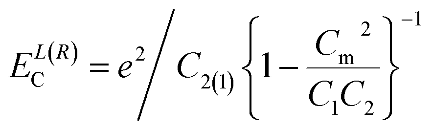 . The charging energy of the right QD is markedly smaller than that of the left QD, probably due to unequal capacitances and different QD size. We summarize the obtained parameters of the DQD (device A) in Table 1 in the ESI.†Fig. 1(d) shows a more detailed map of the bias triangle marked with the blue dashed rectangular in (c), showing clean DQD characteristics for the gate voltages for which we now discuss CP.
We perform charge pumping through DQDs by applying two phase-shifted sinusoidal voltages (ϕ1 and ϕ2) to two gates at VSD ≈ 0 mV, using bias-tees and an arbitrary waveform generator as illustrated in Fig. 1(a). The resulting DC pump current through the DQD is measured by a current–voltage (IV) converter. The mechanism of adiabatic charge pumping using a DQD is explained in ESI, Fig. S2.†9 The occupation number (n, m) of the DQD is varied periodically by applying two sinusoidal modulations of the voltages VL and VR with a 90° phase shift to the plunger gates of the respective QD, resulting in circular periodic trajectories around a triple point in the charge stability diagram. When the path on the stability diagram encircles a triple point, exactly one electron, or one hole, is shuttled per cycle from one contact to the other. The pump current is then expected to be only related to the drive frequency, i.e., I = ±ef, with e an elementary charge, where the polarity of the current is defined by the pump direction.
Fig. 2(a) shows the pump current around the triple points shown in Fig. 1(d) measured as a function of VL and VR at a modulating frequency of f = 5 MHz at an RF power of P = −32 dBm and the bias VSD ≈ 0 V. We find two elliptical regions of roughly constant current in the vicinity of a pair of triple points, highlighted by arrows in Fig. 2(a). The sign of the current is reversed around the second triple point. We optimize the phase between the two applied AC signals to obtain the widest quantized plateaus as a function of VL and VR. Here, the left and right phases are set to ϕ1 = 0° and ϕ2 = 70° (i.e. Δϕ = ϕ1 − ϕ2 = 70°), respectively. Fig. 2(b) shows the line traces of the pump current measured along the dashed line in Fig. 2(a) for f = 3 and 5 MHz. The pump current plateaus are observed at ∼0.48 and 0.8 pA for f = 3 and 5 MHz with respect to the offset current of 25.2 pA in this experiment, respectively, which corresponds accurately to I = ef, within the measurement accuracy of ∼40 fA. As expected, when we increase the amplitude of the RF signal from P = −33 to −31 dBm, the plateaus in the pump current around each triple point are extended (see ESI, Fig. S3†). We note that optimizing the phase shift between the modulated gate voltages is not trivial in this device, likely due to the capacitive coupling between the two gate lines and a non-identical frequency response of the RF components such as the bias-tees and RF cables.
 | ||
| Fig. 2 (a) Pump current generated by the DQD (device A) as a function of VL and VR at f = 5 MHz and P = −32 dBm (VPP = 15.884 mV). (b) Line traces of the pump current along the electron pumping cycle as indicated by the dashed line in (a) for f = 3 and 5 MHz. The expected level of the quantized pumping current, I = ef, is indicated by horizontal dashed lines. (c) Pump current measured at f = 25 MHz and P = −37 dBm (VPP = 8.932 mV). (d) Pump current measured at f = 25 MHz and P = −35 dBm (VPP = 11.245 mV). The insets show the line traces taken along the dashed lines. The pump currents at both triple points are not quantized exactly according to I = ef. | ||
As we increase the pump frequency, the deviation of the pump current from the expected value, I = ef, increases (see ESI, Fig. S4†). Fig. 2(c) and (d) show the current maps for f = 25 and 50 MHz, respectively. As shown in Fig. 2(c), the forward and reversed bias triangles with the positive and negative current form two triangles at each degeneracy point and the pump currents at both triple points are not quantized exactly according to I = ef. For the two frequencies in Fig. 2(c) and (d), we would expect CP currents of 4 and 8 pA, respectively, clearly not reached in both cases, especially well visible in the insets of Fig. 2(c) and (d). The triangular gate dependence of the CP current observed in device A was explained before (ref. 18) as resulting from a non-optimal phase between the two RF signals. However, here it was not possible to find the circular gate dependence expected for the ideal pump phases. This behavior could occur when a mutual gate–gate capacitance (cross-talk) significantly reduces the relative phase difference. An alternative explanation could be asymmetric tunnel couplings between the QDs and the respective reservoirs. In an ideal electron cycle at the triple point, the empty left level goes below the Fermi energy and is filled by the left reservoir. Then, it tunnels to the right dot before the left dot is filled by the right reservoir, resulting in the desired forward current. However, the direction of the current flow is very sensitive to the tunneling dynamics and the time-dependent QD occupations. If the tunnel coupling between the right dot and the right reservoir is much stronger than the coupling between the left dot and left reservoir, an electron fills the right dot first instead of the left dot and tunnels into the left dot to exit the system to the left reservoir, resulting in a reverse current. To account for phase shifts and such non-adiabatic processes, a refined model is needed, which is beyond the scope of this work. Here, we now focus on the first explanation, which suggests that the performance of the CP could be improved by reducing the RF capacitive coupling between the gate lines.17,18,22
To minimize the capacitive coupling between the gate lines, we fabricated a DQD with side gates, with reduced capacitances between the gates due to a significantly increased distance between the gate lines (device B), as shown in Fig. 3(a). A nanowire taken from the same growth-batch as the one used for device A and with a similar diameter is transferred to the SiO2 surface. Source and drain electrodes are separated by 950 nm and a DQD is formed in between. We fabricated multiple side gates to the NW, with a maximally increasing separation between gate lines away from the NW to minimize the capacitive coupling between the side gates. The separation between the left and right gates (VL and VR) are ∼400 nm near the DQD and gradually increases further. Therefore, the distance between the gates near the DQD in device B is four times wider than the uniform bottom gates of 100 nm pitch and 10 μm long in device A (see Fig. 1(a)). We estimate the capacitances between two gates in device A and B to be ∼13 aF and 0.7 aF, respectively, using a simple rectangular parallel plate capacitance model as a crude approximation, showing that the inter-gate capacitance is reduced by almost a factor of 20 in device B compared to device A. The typical resistance of the gate lines is R ∼ 1 kΩ for both device A and B. These result in TRC = RC ∼ 1.3 × 10⁻¹⁴ s and 0.7 × 10⁻¹⁵ s for device A and B, respectively. Similar to device A, we performed measurements with device B at 20 mK and form a DQD with the three gate voltages, VL, VM, and VR as illustrated in Fig. 3(a). Fig. 3(b) displays the DC current of the DQD measured as a function of VR and VL at VSD = 2 mV, showing similar bias triangles as we found in device A, including well resolved excited states. The charging energies of the two QDs are estimated from the charge stability diagrams to yield EC, L = 7.8 meV and EC, R = 11.4 meV for the left and right QDs, respectively. The extracted device parameters can be compared directly to device A in Table 1 of the ESI.†
 | ||
| Fig. 3 (a) SEM image of side gated InAs DQD device (device B) and a diagram of the measurement circuit. All side gates are designed with a maximum separation to reduce capacitive coupling. Three gates with the applied voltage VL, VM, and VR are used to form a DQD in the nanowire by setting VM = –4.7 V. (b) DC current through the InAs DQD measured as a function of the two gate voltages, VL and VR with a source-drain bias of VSD = 2 mV. | ||
We now discuss the achieved charge pumping for device B, for which we have optimized the phase shift and RF power of the two sinusoidal pump voltages (ESI, Fig. S5†). The RF signal phases have a significant impact in device B, in stark contrast to our findings for device A, consistent with a reduced capacitive cross-talk in this design. We find the optimal gate phases at ϕ1 = 0° and ϕ2 = 90°, respectively, at which the device shows the best quantized current plateaus, as one would expect in the case without cross-talk. Fig. 4(a) and (b) show the pump current around a pair of triple points of the DQD measured as a function of VL and VR at a modulation frequency f = 20 and 30 MHz, respectively, significantly higher than for device A and an RF power of P = −32 dBm. Two elliptical shapes with positive and negative currents around the respective triple point exhibit a shape much closer to the ideal case, again in stark contrast to device A. The elliptical instead of circular shapes are likely caused by asymmetric lever arms of the gates. The current plateaus correspond very well to the expected value of I = ef. These findings do not change significantly up to f = 30 MHz, as shown in Fig. 4(b). Fig. 4(c) and (d) display the line traces of the pump current for f = 20 MHz, along the electron and hole pumping cycles indicated by the dashed lines in (a). Though there is a smoothly changing background current, the device shows the quantized pumping current around I = ±ef = ±3.2 pA, indicated by the blue horizontal lines shown in Fig. 4(c) and (d). We also measure the pump current at a different pair of triple points for f = 30 MHz and observe similar characteristics, as shown in Fig. 4(e). Fig. 4(f) and (g) show the line traces taken along the dashed lines (C and D) in Fig. 4(e). The pump current plateaus are observed around I = ±ef = ±4.8 pA, as expected for an ideal charge pump. As shown in Fig. 4(h), the CP current at these gate voltages scales linearly with the pump frequency up to 30 MHz, with a slope of dI/df = ±e, as expected. We note that at frequencies larger than f = 30 MHz, the pump current again starts to deviate from the fundamental relation I = ±ef. Nevertheless, the quantization of the pump current is significantly improved in device B compared to device A in the range up to f = 30 MHz.
 | ||
| Fig. 4 Pump current at the triple points measured as a function of VL and VR at (a) f = 20 MHz and (b) f = 30 MHz, both with P = −32 dBm (VPP = 15.884 mV). (c) and (d) Line traces of the pump current for f = 20 MHz along the electron and hole pumping cycle as indicated by the dashed lines (A and B) in (a). The expected quantized current value of I = ±ef (= ±3.2 pA) is indicated by horizontal dashed lines. (e) Pump current measured at a different pair of triple points for f = 30 MHz. (f) and (g) The line traces of the pump current along the electron and hole pumping cycles indicated by the dashed lines (C and D) in (e). (h) Frequency dependence of the pump current. | ||
To check whether the asymmetric QD configuration affects the charge pump performance in our devices, we tuned the charging energies of the left and right QDs of device B to be comparable with that of device A. Table 1 and Fig. S6 in the ESI† show that the charging energy of the left QD is larger than that of the right QD, thus its QD formation is now similar to device A; the charging energies of the left and right QD are ELC ≈ 16 meV and ERC ≈ 10 meV, respectively. We observed very similar behaviors with the first tuning condition of device B, as shown in Fig. S6 in the ESI.† Future devices for high speed CP will benefit from such design improvements related to the capacitive cross-talk, like side gates from alternating sides of the nanowire.
The optimization of the gate line geometries is a very general approach that can in principle be employed for all CP platforms. In earlier work by Fuhrer et al.15 in which InAs DQDs were fabricated on a heavily doped Si substrate and measured with DC lines for the pulse sequences, the CP operating frequency was limited to around 3 MHz and exhibited less pronounced plateaus. This suggests that capacitive coupling and RF cutoff frequencies limit higher frequency adiabatic CP. In previous experiments on non-adiabatic CP with a single gate,16 quantized CP on a single InAs QD was possible up to frequencies larger than 1 GHz using improved high frequency cabling and a reduction of the RF losses by using undoped Si substrates. With a single gate and for non-adiabatic CP, the phase of the RF signal is irrelevant, allowing these significantly larger frequencies.
The unique advantages of a semiconductor platform come from the insight that, in addition to the capacitive cross-talk between the gate lines, other parameters are relevant for adiabatic DQD quantized CP as well. For example, the dwell times on the QDs is often characterized by the RC time constants of the tunnel barriers, where R and C are an effective resistance and capacitance characterizing the charging dynamics of the QDs. The error rate caused by missed tunneling events is expected to increase exponentially with increasing RC values for the same operation frequency, roughly ∼exp(1/RCf).23,41,42 Recently, in a graphene DQD device with a factor-of-ten smaller value of the RC time constant compared to conventional metal-oxide junction devices, GHz adiabatic quantized CP has been demonstrated.23 In this device, well-separated side gates were used-in accordance with our results. However, in graphene, the tunnel barriers are formed by constrictions and cannot be controlled by gate voltages, because graphene is a semimetal. In contrast, a semiconductor can have gate tunable barriers, which, in principle, should allow one to tune also the RC time and thus to obtain significantly higher pump frequencies.
To further improve the charge pump performance in DQDs with multiple gates, it is essential to reduce the cross-talk of gate voltages to QD potentials and interdot tunnel couplings. Recently, an efficient calibration technique for reducing such cross-talk in multi-dot systems with multiple gates has been developed by introducing virtual gates as linear combinations of physical gate voltages.43–47 As shown in our experiments, a minimal cross-talk between gate lines and DQDs is essential for CP, so that it should also be possible to employ the technique of virtual gates to improve CP, resulting in additionally optimizing the relative amplitudes of the drive signals.
Conclusions
We have demonstrated adiabatic quantized charge pumping in InAs nanowire DQDs with two different device geometries, one with an array of narrow bottom gates and one with well-separated side gates for which we have investigated the pump current as a function of the modulation frequency and amplitude. For the closely spaced bottom gate array, the charge pumping is quantized accurately only up to a few MHz, with CP current patterns consistent with a non-ideal phase between the two RF signals, which cannot be corrected due to a strong capacitive coupling between the bottom gates. For a very similar device with well-separated side gates, we find close to ideal pump current patterns and quantized current levels for frequencies up to 30 MHz. Our experiments demonstrate that it is essential to optimize the device geometry for the accurate operation of high speed single electron adiabatic CPs, including the gate feed lines.Conflicts of interest
There are no conflicts to declare.Acknowledgements
M. J. thanks H.-S. Sim for helpful discussions. This work is supported by the National Research Foundation of Korea (NRF) Grant funded by the Korean Government (NRF-2020R1A2C1008448, 2021R1A2C1011046, and 2022M3E4A1069445) and DGIST R&D Program of the Ministry of Science, ICT, Future Planning (20-CoE-NT-02, 19-CoE-NT-01 and 22-NT-01). MHB is supported by Grant nos KRISS-2021-GP2021-0001, 2021R1A2C3012612, and SRC2016R1A5A1008184. CS & AB acknowledge financial support from Swiss Nanoscience Institute, the ERC projects QUEST & TopSupra and the Swiss National Science Foundation (SNF) through various grants, including the NCCR-QSIT and SPIN. M. J. L. is supported by Next-Generation Intelligent Semiconductor Technology Development Program through the National Research Foundation of Korea (NRF) funded by Ministry of Science and ICT (2020M3F3A2A02082437). M. J. thanks Hyeon Jeong Lee, Hwan Soo Jang and Bong Ho Lee at INST of DGIST for device fabrication and helpful discussions.References
- A. Chatterjee, P. Stevenson, S. De Franceschi, A. Morello, N. de Leon and F. Kuemmeth, Nat. Rev. Phys., 2021, 3, 157–177 CrossRef.
- M. Veldhorst, C. H. Yang, J. C. C. Hwang, W. Huang, J. P. Dehollain, J. T. Muhonen, S. Simmons, A. Laucht, F. E. Hudson, K. M. Itoh, A. Morello and A. S. Dzurak, Nature, 2015, 526, 410–414 CrossRef CAS PubMed.
- N. Feltin and F. Piquemal, Eur. Phys. J.: Spec. Top., 2009, 172, 267–296 Search PubMed.
- J. P. Pekola, O.-P. Saira, V. F. Maisi, A. Kemppinen and M. Mottonen, Rev. Mod. Phys., 2013, 85, 1421–1472 CrossRef.
- F. Stein, H. Scherer, T. Gerster, R. Behr, M. Gotz, E. Pesel, C. Leicht, N. Ubbelohde, T. Weimann, K. Pierz, H. W. Schumacher and F. Hohls, Metrologia, 2017, 54, S1–S8 CrossRef CAS.
- S. P. Giblin, A. Fujiwara, G. Yamahata, M.-H. Bae, N. Kim, A. Rossi, M. Mottonen and M. Kataoka, Metrologia, 2019, 56, 044004–044020 CrossRef CAS.
- S. Das and V. Shpitalnik, Europhys. Lett., 2008, 83, 17004–17009 CrossRef.
- M. Alos-Palop, R. P. Tiwari and M. Blaauboer, Phys. Rev. B, 2014, 89, 045307–045311 CrossRef.
- H. Pothier, P. Lafarge, C. Urbina, D. Esteve and M. H. Devoret, Europhys. Lett., 1992, 17, 249–254 CrossRef.
- L. P. Kouwenhoven, A. T. Johnson, N. C. van der Vaart, C. J. P. M. Harmans and C. T. Foxon, Phys. Rev. Lett., 1991, 67, 1626–1629 CrossRef CAS PubMed.
- M. D. Blumenthal, B. Kaestner, L. Li, S. Giblin, T. J. B. M. Janssen, M. Pepper, D. Anderson, G. Jones and D. A. Ritchie, Nat. Phys., 2007, 3, 343–347 Search PubMed.
- B. Kaestner, V. Kashcheyevs, S. Amakawa, M. D. Blumenthal, L. Li and T. J. B. M. Janssen, Phys. Rev. B, 2008, 77, 153301–153304 CrossRef.
- M. Kataoka, J. D. Fletcher, P. See, S. P. Giblin, T. J. B. M. Janssen, J. P. Griffithis, G. A. C. Jones, I. Farrer and D. A. Ritchie, Phys. Rev. Lett., 2011, 106, 126801–126804 CrossRef CAS PubMed.
- S. P. Giblin, M. Kataoka, J. D. Fletcher, P. See, T. J. B. M. Janssen, J. P. Griffiths, G. A. C. Jones, I. Farrer and D. A. Richie, Nat. Commun., 2012, 3, 930–935 CrossRef CAS PubMed.
- A. Fuhrer, C. Fasth and L. Samuelson, Appl. Phys. Lett., 2007, 91, 052109–052111 CrossRef.
- S. d'Hollosy, M. Jung, A. Baumgartner, V. A. Guzenko, M. H. Madsen, J. Nygård and C. Schönenberger, Nano Lett., 2015, 15, 4585–4590 CrossRef PubMed.
- S. J. Chorley, J. Frake, C. G. Smith, G. A. C. Jones and M. R. Buitelaar, Appl. Phys. Lett., 2012, 100, 143104–143106 CrossRef.
- B. Roche, R.-P. Riwar, B. Voisin, E. Dupont-Ferrier, R. Wacquez, M. Vinet, M. Sanquer, J. Slettstoesser and X. Jehl, Nat. Commun., 2012, 4, 1581–1585 CrossRef PubMed.
- A. Fujiwara, N. M. Zimmerman, Y. Ono and Y. Takahashi, Appl. Phys. Lett., 2004, 84, 1323–1325 CrossRef CAS.
- G. Yamahata, K. Nichiguchi and A. Fujiwara, Nat. Commun., 2014, 5, 5038–5044 CrossRef CAS PubMed.
- A. R. Mills, D. M. Zajac, M. J. Gullans, F. J. Schupp, T. M. Hazard and J. R. Petta, Nat. Commun., 2019, 10, 1063–1068 CrossRef CAS PubMed.
- R. Murray, J. K. Perron, M. D. Stewart, A. L. Levy, P. See, S. P. Giblin, J. D. Fletcher, M. Kataoka and N. M. Zimmerman, J. Appl. Phys., 2020, 127, 094301–094311 CrossRef CAS.
- M. R. Connolly, K. L. Chiu, S. P. Giblin, M. Kataoka, J. D. Fletcher, C. Chua, J. P. Griffiths, G. A. C. Jones, V. I. Falko, C. G. Smith and T. J. B. M. Janssen, Nat. Nanotechnol., 2013, 8, 417–420 CrossRef CAS PubMed.
- S. Csonka, L. Hofstetter, F. Freitag, S. Oberholzer and C. Schönenberger, Nano Lett., 2008, 8, 3932–3935 CrossRef CAS PubMed.
- S. Nadj-Perge, S. M. Frolov, E. P. A. Bakkers and L. P. Kouwenhoven, Nature, 2010, 468, 1084–1087 CrossRef CAS PubMed.
- K. D. Petersson, L. W. McFaul, M. D. Schroer, M. Jung, J. M. Taylor, A. A. Houck and J. R. Petta, Nature, 2012, 490, 380–383 CrossRef CAS PubMed.
- T. R. Hartke, Y.-Y. Liu, M. J. Gullans and J. R. Petta, Phys. Rev. Lett., 2018, 120, 097701–097705 CrossRef CAS PubMed.
- P. D. Nissen, T. S. Jespersen, K. Grove-Rasmussen, A. Marton, S. Upadhyay, M. H. Madsen, S. Csonka and J. Nygård, J. Appl. Phys., 2012, 112, 084323–084329 CrossRef.
- M.-T. Deng, S. Vaitiekenas, E. Prada, P. San-Jose, J. Nygard, P. Krogstrup, R. Aguado and C. M. Marcus, Phys. Rev. B, 2018, 98, 085125–085134 CrossRef CAS.
- D. M. T. Van Zanten, D. Sabonis, J. Suter, J. I. Vayrynen, T. Karzig, D. I. Pikulin, E. C. T. O'Farrell, D. Razmadze, K. D. Petersson, P. Krogstrup and C. M. Marcus, Nat. Phys., 2020, 16, 663–668 Search PubMed.
- S. Baba, C. Junger, S. Matsuo, A. Baumgartner, Y. Sato, H. Kamata, K. Li, S. Jeppesen, L. Samuelson, H. Q. Xu, C. Schönenberger and S. Tarucha, New J. Phys., 2018, 20, 063021–063028 CrossRef.
- L. Hoffstetter, S. Csonka, J. Nygård and C. Schönenberger, Nature, 2009, 461, 960–963 CrossRef PubMed.
- A. Bordoloi, V. Zannier, L. Sorba, C. Schönenberger and A. Baumgartner, Commun. Phys., 2020, 3, 135–141 CrossRef.
- S. Dorsch, B. Dalelkhan, S. Fahlvik and A. M. Burke, Nanotechnology, 2019, 30, 144002–144008 CrossRef CAS PubMed.
- M. H. Madsen, P. Krogstrup, E. Johnson, S. Venkatesan, E. Muhlbauer, C. Scheu, C. B. Sorensen and J. Nygård, J. Cryst. Growth, 2013, 364, 16–22 CrossRef CAS.
- H. Shtrikman, R. Popovitz-Biro, A. Kretinin, L. Houben, M. Heiblum, M. Bukala, M. Galicka, R. Buczko and P. Kacman, Nano Lett., 2009, 9, 1506–1510 CrossRef CAS PubMed.
- K. Ono, D. G. Austing, Y. Tokura and S. Tarucha, Science, 2002, 297, 1313–1317 CrossRef CAS PubMed.
- J. Wang, S. Huang, Z. Lei, D. Pan, J. Zhao and H. Q. Xu, Appl. Phys. Lett., 2016, 109, 053106–053109 CrossRef.
- F. S. Thomas, M. Nilsson, C. Ciaccia, C. Junger, F. Rossi, V. Zannier, L. Sorba, A. Baumgartner and C. Schönenberger, Phys. Rev. B, 2021, 104, 115415–115424 CrossRef CAS.
- W. G. Van der Wiel, S. De Franceschi, J. M. Elzerman, T. Fujisawa, S. Tarucha and L. P. Kouwenhoven, Rev. Mod. Phys., 2003, 75, 1–22 CrossRef CAS.
- M. Keller, J. M. Martinis, N. Zimmerman and A. Steinbach, Appl. Phys. Lett., 1996, 69, 1804–1806 CrossRef CAS.
- J. M. Martinis, M. Nahum and H. D. Jensen, Phys. Rev. Lett., 1994, 72, 904–907 CrossRef CAS PubMed.
- T. Hensgens, T. Fujita, L. Janssen, X. Li, C. J. Van Diepen, C. Reichl, W. Wegscheider, S. Das Sarma and L. M. K. Vandersypen, Nature, 2017, 548, 70–73 CrossRef CAS PubMed.
- C. Volk, A. M. J. Zwerver, U. Mukhopadhyay, P. T. Eendebak, C. J. Van Diepen, J. P. Dehollain, T. Hensgens, T. Fujita, C. Reichl, W. Wegscheider and L. M. K. Vandersypen, npj Quantum Inf., 2019, 5, 29–36 CrossRef.
- A. R. Mills, D. M. Zajac, M. J. Gullans, F. J. Schupp, T. M. Hazard and J. R. Petta, Nat. Commun., 2019, 10, 1063–1068 CrossRef CAS PubMed.
- T. Botzem, M. D. Shulman, S. Foletti, S. P. Harvey, O. E. Dial, P. Bethke, P. Cerfontaine, R. P. G. McNeil, D. Mahalu, V. Umansky, A. Ludwig, A. Wieck, D. Schuh, D. Bougeard, A. Yacoby and H. Bluhm, Phys. Lett. Appl., 2018, 10, 054026–054037 CAS.
- T.-K. Hsiao, C. J. Van Diepen, U. Mukhopadhyay, C. Reichl, W. Wegscheider and L. M. K. Vandersypen, Phys. Lett., Appl., 2020, 13, 054018–054026 CAS.
Footnotes |
| † Electronic supplementary information (ESI) available. See https://doi.org/10.1039/d2na00372d |
| ‡ S. J. A. and M.-H. B. contributed equally to this work. |
| This journal is © The Royal Society of Chemistry 2022 |