
 Open Access Article
 This Open Access Article is licensed under a Creative Commons Attribution-Non Commercial 3.0 Unported Licence
Bi2O2Se-based integrated multifunctional optoelectronics†
Dharmendra
Verma
 a,
Bo
Liu
b,
Tsung-Cheng
Chen
a,
Lain-Jong
Li
c and
Chao-Sung
Lai
*adef
a,
Bo
Liu
b,
Tsung-Cheng
Chen
a,
Lain-Jong
Li
c and
Chao-Sung
Lai
*adef
aDepartment of Electronic Engineering, Chang-Gung University, Taoyuan 33302, Taiwan. E-mail: cslai@mail.cgu.edu.tw; Tel: +886-3-2118800 ext. 5786
bFaculty of Information Technology, College of Microelectronics, Beijing University of Technology, Beijing 100124, People's Republic of China
cDepartment of Mechanical Engineering, University of Hong Kong, Pokfulam Road, 999077, Hong Kong
dDepartment of Nephrology, Chang Gung Memorial Hospital, Linkou, 33302, Taiwan
eDepartment of Materials Engineering, Ming-Chi University of Technology, New Taipei City 24301, Taiwan
fArtificial Intelligence Research Center, Chang Gung University, Taoyuan 33302, Taiwan
First published on 1st August 2022
Abstract
The prominent light–matter interaction in 2D materials has become a pivotal research area that involves either an archetypal study of inherent mechanisms to explore such interactions or specific applications to assess the efficacy of such novel phenomena. With scientifically controlled light–matter interactions, various applications have been developed. Here, we report four diverse applications on a single structure utilizing the efficient photoresponse of Bi2O2Se with precisely tuned multiple optical wavelengths. First, the Bi2O2Se-based device performs the function of optoelectronic memory using UV (λ = 365 nm, 1.1 mW cm−2) for the write-in process with SiO2 as the charge trapping medium followed by a +1 V bias for read-out. Second, associative learning is mimicked with wavelengths of 525 nm and 635 nm. Third, using similar optical inputs, functions of logic gates “AND”, “OR”, “NAND”, and “NOR” are realized with response current and resistance as outputs. Fourth is the demonstration of a 4 bit binary to the decimal converter using wavelengths of 740 nm (LSB), 595 nm, 490 nm, and 385 nm (MSB) as binary inputs and output response current regarded as equivalent decimal output. Our demonstration is a paradigm for Bi2O2Se-based devices to be an integral part of future advanced multifunctional electronic systems.
Introduction
The development of optoelectronic memory (OEM) is one of the key applications that emerged from the novel phenomenon of light–matter interaction (LMI) and has become more crucial due to its merits over conventional resistive memory in terms of data storage and fast processing together with optical sensing. The OEM cell receives the information during the write-in (or programming) process through the exposure of light of appropriate wavelength and subsequently read-out (erasing) of stored information by means of an electrical mechanism. The low voltage requirement for the operation of OEM is advantageous not only in data storage but also in the secured transportation of information. Moreover, OEM further adds enhanced storage capacity through the implementation of multilevel data storage accomplished by improving the ratio of high resistance state (HRS) and low resistance state (LRS). The optically activated switching in OEM improves bandwidth and overcomes the electrical loss in data transmission.1–5 Different materials have been extensively explored to demonstrate optoelectronic memory, such as semiconductor nano materials (0D,6 1D,7 2D8), polymers,9 organic,10,11 and heterostructures of such materials.4,12–15 Furthermore, in some studies, phase change materials have been used to demonstrate optoelectronic memory.16,17 Charge trapping plays a vital role in the implementation of optical memory. The charge trapping characteristics of graphene and MoS2 were studied by graphene/hBN/MoS2 structures showing different hysteresis curves with variations in the thickness of MoS2 layers.18 A single-layer MoS2-based photonic memory device has been used both for optical sensing and channel materials, and AuNPs are used as charge trapping layers.19 The OEM proof of concept has been explained by incorporating three distinct 2D materials CuIn7Se11, InSe, and MoS2via trapping and releasing photogenerated charge carriers with the gating effect. Additionally, an array of such devices that resembles conventional charge-coupled devices (CCDs) for image sensors was studied.20 The photoresponsive properties of the hybrid structure of graphene and MoS2 are used to realize optoelectronic memory. However, the high electrical conductivity of graphene yields a high dark current and hence a low ON/OFF ratio (<2) and is a challenge for the success of the structure.21 Functionalization of the MoS2/dielectric interface produces an artificially structured charge trap layer that is used to implement monolayer MoS2-based optoelectronic memory with an improved ON/OFF ratio (4700) and a long storage lifetime (104 s).22 In recent studies, Alexey Lipatov et al. have reported an improved ON/OFF ratio (105) with (ON state) and without (OFF state) light illumination over MoS2–Pb (Zr, Ti) O3 structure for optical memory.23 Feng Gao et al. reported a multibit optical memory with low optical power (0.32 nW) based on the SnS2/h-BN/graphene structure.15 Among recent reports, Yuqian Chen et al. demonstrated a heterostructure of PtS2/h-BN/graphene as multibit optoelectronic memory, which performed up to 74 differentiable states (>6 bits) via controlled linear conductance using light pulses.24In concern with multifunction, specific operations are also performed within the memory devices such as arithmetical operation,1,25 logic operation (function of digital logic gates: “AND”, “OR”, “NAND”, “NOR”),2,16,26–28 and Pavlovian associative learning process.29–31 Moreover, photomemrister28,32,33 and photonic synapse34 were also studied and reported. Although substantial efforts and success have been reported, optoelectronic memory devices with multifunction operation by new materials/structures are in everlasting demand. Bi2O2Se, a new layered 2D material, has been paid much attention during the last half decade because of its ultra-high mobility (>20![[thin space (1/6-em)]](https://www.rsc.org/images/entities/char_2009.gif) 000 cm2 V−1 s−1 at 2 K), vigorous band gap (1.9 eV for monolayer), and excellent air stability showing enough potential of exceeding 2D materials.35 Compared to other van der Waals 2D materials, Bi2O2 Se is composed of alternated stacked layers of Bi2O22+ and Se2− layers interacting with weekly electrostatic forces. Competent light absorption property and moderate band gap (∼0.8 eV) make Bi2O2Se a favorable material for optoelectronic applications.36–38 Major reported synthesis methods are CVD,35 wet chemical process,39 precursor co-evaporation,40 hydrothermal process,41,42 solution assisted method,43 and organic-CVD.44 Significant efforts have been made in the synthesis of Bi2O2Se to improve the grain size to make it more applicable. The major reports regarding grain size include micrometer (>200 μm),35 millimeter,45 and wafer scale size.47 Along with optical property, Bi2O2Se also represents ferroelectric/ferroelastic property,48 inherent bolometric effect,49 and phase transition under compression (30 GPa).50 Among various properties of Bi2O2Se, optical sensing has been widely explored in the development of phototransistors45,47,51,52 and photodetectors.49,53 In other recent reports, Bi2O2Se has been found in vast fields of applications: transistor,54,55 polymer solar cell,56 broad band photodetector (IR to THz),57 coincidence detection,58 and memristors.59 Wu et al. have explored high electron mobility and quantum oscillations in layered Bi2O2Se and fabrication of top gate FET showing ON/OFF ratio >106 and subthreshold swing 65 mV per decade (at room temperature) with Hall mobility 450 cm2 V−1 s−1.60 The heterostructure of Bi2O2Se/graphene was reported for the demonstration of photodetector and short channel FET (50 nm) by Tan et al.61 In another study by Yang et al., Bi2O2Se/graphene hybrid structure was utilized to demonstrate multifunctional optoelectronics, including photodetector, optical synapse, and logic gate by the control of optical wavelengths.62 Some recent reports focused on Bi2O2Se-based heterostructures: Bi2O2Se/Bi2Se3,63 Bi2Te2Se/Bi2O2Se,64 Bi2O2Se/TMDs,65 and Bi2O2Se/CsPbBr3,66 showing potential use of Bi2O2Se in combination with other materials for optoelectronic applications. Although Bi2O2Se shows competent light sensing property in a wide band, multifunctional optoelectronic by only the Bi2O2Se based structure has not been explored so far.
000 cm2 V−1 s−1 at 2 K), vigorous band gap (1.9 eV for monolayer), and excellent air stability showing enough potential of exceeding 2D materials.35 Compared to other van der Waals 2D materials, Bi2O2 Se is composed of alternated stacked layers of Bi2O22+ and Se2− layers interacting with weekly electrostatic forces. Competent light absorption property and moderate band gap (∼0.8 eV) make Bi2O2Se a favorable material for optoelectronic applications.36–38 Major reported synthesis methods are CVD,35 wet chemical process,39 precursor co-evaporation,40 hydrothermal process,41,42 solution assisted method,43 and organic-CVD.44 Significant efforts have been made in the synthesis of Bi2O2Se to improve the grain size to make it more applicable. The major reports regarding grain size include micrometer (>200 μm),35 millimeter,45 and wafer scale size.47 Along with optical property, Bi2O2Se also represents ferroelectric/ferroelastic property,48 inherent bolometric effect,49 and phase transition under compression (30 GPa).50 Among various properties of Bi2O2Se, optical sensing has been widely explored in the development of phototransistors45,47,51,52 and photodetectors.49,53 In other recent reports, Bi2O2Se has been found in vast fields of applications: transistor,54,55 polymer solar cell,56 broad band photodetector (IR to THz),57 coincidence detection,58 and memristors.59 Wu et al. have explored high electron mobility and quantum oscillations in layered Bi2O2Se and fabrication of top gate FET showing ON/OFF ratio >106 and subthreshold swing 65 mV per decade (at room temperature) with Hall mobility 450 cm2 V−1 s−1.60 The heterostructure of Bi2O2Se/graphene was reported for the demonstration of photodetector and short channel FET (50 nm) by Tan et al.61 In another study by Yang et al., Bi2O2Se/graphene hybrid structure was utilized to demonstrate multifunctional optoelectronics, including photodetector, optical synapse, and logic gate by the control of optical wavelengths.62 Some recent reports focused on Bi2O2Se-based heterostructures: Bi2O2Se/Bi2Se3,63 Bi2Te2Se/Bi2O2Se,64 Bi2O2Se/TMDs,65 and Bi2O2Se/CsPbBr3,66 showing potential use of Bi2O2Se in combination with other materials for optoelectronic applications. Although Bi2O2Se shows competent light sensing property in a wide band, multifunctional optoelectronic by only the Bi2O2Se based structure has not been explored so far.
In this report, we explore the spectacular light sensing characteristic of Bi2O2Se by the implementation of four distinct applications, namely optoelectronic memory, associative learning process, digital logic, and 4 bit binary to the decimal converter by means of precisely tuned multiple optical wavelengths over a single Bi2O2Se based structure. The generation of photonic charge carriers under exposure of UV (λ = 365 nm, 1.1 mW cm−2) and trapping/detrapping of these charge carriers via bias potential reveals the operation of OEM. The effect of exposure dose, optical power density, and waiting time over the performance are also investigated. Next, the associative learning process is demonstrated by considering the drooling of a dog as an example. The wavelengths 635 nm (2.0 mW cm−2) and 525 nm (2.0 mW cm−2) were adopted as neutral stimuli (NS) and unconditional stimuli (US), respectively, while the level of output current determines the behavioral change of the dog. We further realize the function of logic gates by utilizing the same wavelengths as digital inputs while the response current level shows the output for “AND” and “OR” gates, and the corresponding resistance level shows the output for “NAND”, and “NOR” gates. The implementation of a 4 bit binary to decimal converter is proposed and realized for the first time. The operation is accomplished by considering four different wavelengths 740 nm (LSB), 595 nm, 490, and 385 nm (MSB) as binary inputs (from “0000” to “1111”) while the response current is regarded as equivalent decimal output (from “0” to “15”). Our demonstration evidences a single Bi2O2Se based structure having enough ability to perform multiple optoelectronic functions.
Results and discussion
The Bi2O2Se nanoplates were synthesized over a MICA substrate via a well-accepted low-pressure chemical vapor deposition (LPCVD) method using Bi2O3 and Bi2Se3 as precursor materials and Ar as the carrier gas with a pressure condition of 100 torr. Later, the synthesized Bi2O2Se nanoplates were transferred to a SiO2/Si substrate (for device fabrication) by PMMA, PDMS sheets, and a water assisted method (details are available in the Experimental section).67Fig. 1a shows a schematic view of the layered structure of Bi2O2Se with a color difference for constituent atoms where gray balls are Se, red balls are O, and pink balls are Bi. The schematic represents four layers with a total thickness of 24.32 Å. The thickness of the monolayer Bi2O2Se is 6.08 Å.35 The lateral gap between two successive Se atoms is 3.88 Å. Raman spectroscopy (Fig. 1b) was carried out for as-grown Bi2O2Se nanoplates over the MICA substrate, displaying a major peak A1g2 = 158 cm−1, which confirms the growth of the Bi2O2Se material, consistent with previous reports.35,45 Two other peaks with comparatively low intensities observed at 217 and 233 cm−1 due to out-of-plane vibrations of “O” atoms are associated with α-Bi2O3 and β-Bi2O3 phases, respectively.46 The atomic force microscopy (AFM) analysis of Bi2O2Se nanoplates (Fig. 1c) shows that the thickness of Bi2O2Se was ∼6 nm (Fig. 1d), revealing the number of layers ∼9 (monolayer thickness of Bi2O2Se = 0.608 nm). Fig. 1e represents the presence of constituent elements “Bi”, “O”, and “Se” confirmed by EDS spectra in view of the corresponding peaks. There are some other peaks for Si (substrate) and Au (to make the surface conductive for FESEM analysis). The elemental weight and atomic percentage are added in the inset. EDS mapping confirms the qualitative chemical composition of Bi2O2Se nanoplate, electron image (Fig. 1f with the area selected for EDS mapping shown in yellow color), and corresponding elemental mapping images showing the uniform distribution of “Bi” (Fig. 1g-1), “O” (Fig. 1g-2), “Se” (Fig. 1g-3) elements. The dimensions (length & width) of the Bi2O2Se nanoplate were measured to be 22 μm and 22 μm, respectively, which shows that the Bi2O2Se nanoplate was almost square in shape. The Bi2O2Se surface was observed without any processing residue over it, indicating its suitability for device fabrication. Fig. 1h shows high-resolution transmission electron microscopy (HRTEM) image of the Bi2O2Se lattice, which confirms high crystallinity in structure and resembles the theoretical depiction. A schematic diagram of the device structure is shown in Fig. 1i. The Bi2O2Se-based device was fabricated with palladium (Pd) as the metal contact and p + Si as the back gate electrode. For the back gate metal contact, aluminum (Al) was used (not shown in the figure). The OM image of the top view of the fabricated device (inset shows the complete view of the device) is presented in Fig. 1j.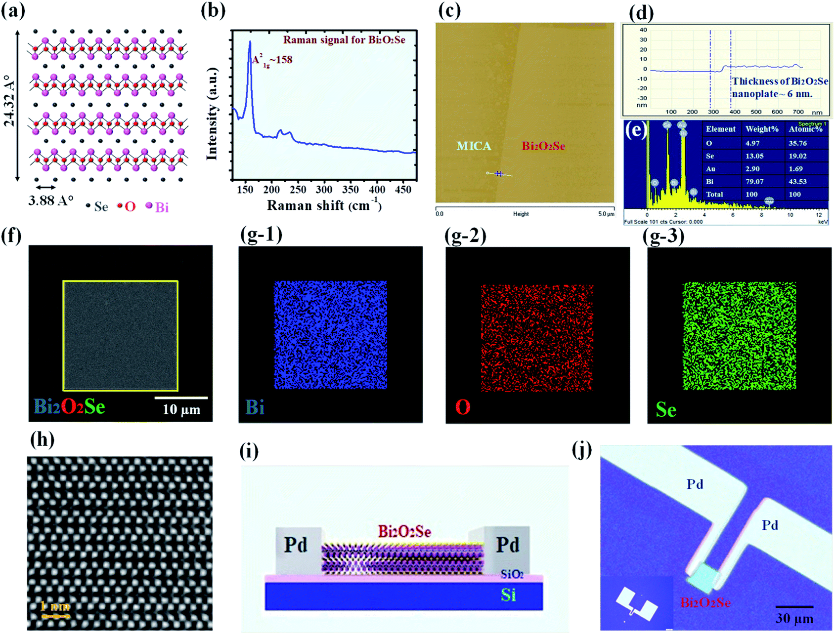 | ||
| Fig. 1 Bi2O2Se material characterization and device fabrication. (a) A schematic view of the layered crystal structure of Bi2O2Se (representing four layers with gray, red, and pink balls for “Se”, “O”, and “Bi” respectively). (b) Raman spectroscopy of the Bi2O2Se nanoplate using a 532 nm laser (A1g2 = 158 cm−1). (c) AFM analysis of the Bi2O2Se nanoplate as grown over the MICA substrate, and (d) thickness measured ∼6 nm (∼9 layers). (e) EDS spectra representing compositional elements: Bi, O, and Se of Bi2O2Se with additional peaks for Si (substrate) and Au (2 nm coating for surface modification). (f) Electron image of the Bi2O2Se nanoplate and corresponding elemental maps for Bi (g-1), O (g-2), and Se (g-3). (h) Cross-sectional HRTEM image of Bi2O2Se with a scale bar 1 nm. (i) Schematic view of the Bi2O2Se based device. (j) OM image of top view of fabricated device with Pd as metal contact on SiO2/Si (inset: full top view of structure). | ||
Optoelectronic memory
The Bi2O2Se-based device is first utilized to demonstrate the operation of optoelectronic memory.19–22 The operating principle of optoelectronic memory is based on the trapping of charge (preferably electrons) generated by controlled optical power and the subsequent detrapping of charge upon application of bias voltage. The complete function of optoelectronic memory includes three major steps: first is the trapping of photogenerated charge (regarded as storing the information, writing: optical method), second is the waiting time (WT: the time during which the charge remains trapped or information retention period: electrical method, by applying back gate bias), and third is the detrapping of charge (regarded as the extraction of information, reading: electrical method, by applying a voltage between the source and drain). A material with the ability to generate electron–hole pairs by absorbing energy from photoexcitation is termed a photoactive material (the active layer within a device) and is the core unit of optoelectronic memory. The material used to trap such photonically produced charge is termed as trapping material (the trapping layer within a device) and is the second key unit of optoelectronic memory. The active layer can also function as a trapping layer.20,22 In our structure, Bi2O2Se has been considered an active layer, while SiO2 beneath Bi2O2Se is considered a trapping layer. Since Bi2O2Se shows a good photoresponse,45,51 its selection as an active layer in the structure of optoelectronic memory is reasonable, while the presence of trapping sites (due to dangling bonds)68 over the surface of SiO2 makes it suitable for charge trapping medium.Fig. 2(a)–(c) depicts the energy band diagram (with Schottky barrier profile) to explain the mechanism of optoelectronic memory involving charge trapping, WT, and detrapping of charge. A potential of +10 V is applied on the back gate throughout the process. This potential helps in the formation of potential wells in the trapping layer. During write-in, a UV light was applied over the device. The photons of the light pulse absorbed by the active layer (Bi2O2Se) generate a number of electron–hole (e–h) pairs. These photonically generated electrons become trapped in the trapping sites (between Schottky barriers ϕb1 and ϕb2) available at the Bi2O2Se/SiO2 interface,68 while holes move through the Schottky barrier between the metal (Pd) semiconductor interface (ϕb1 and ϕb2) available on both sides (Fig. 2a). After that, the device was held in a sufficiently dark condition with an applied back gate bias. The trapped electrons (on the surface of the SiO2 interface) remain over a span of time known as WT, which represents the storage of information (Fig. 2b). Moreover, this WT is a significant parameter for both data and image processing in real time.20 After completion of the WT, a read-out bias (+1 V) is applied (between end point terminals S/D). Due to this read-out bias, the Schottky barrier on one side (ϕb2) becomes reverse biased (preventing leakage of charge or loss of information), while the other Schottky barrier (ϕb1) turns in the forward bias condition. The forward biased Schottky barrier (ϕb1) lowers the barrier height and allows the trapped electrons to move out (Fig. 2c). This step in which the trapped electrons are released is termed as read-out or receiving of stored information. The response current obtained by these electrons is regarded as the reading of information, which is the last step in the function of optoelectronic memory.
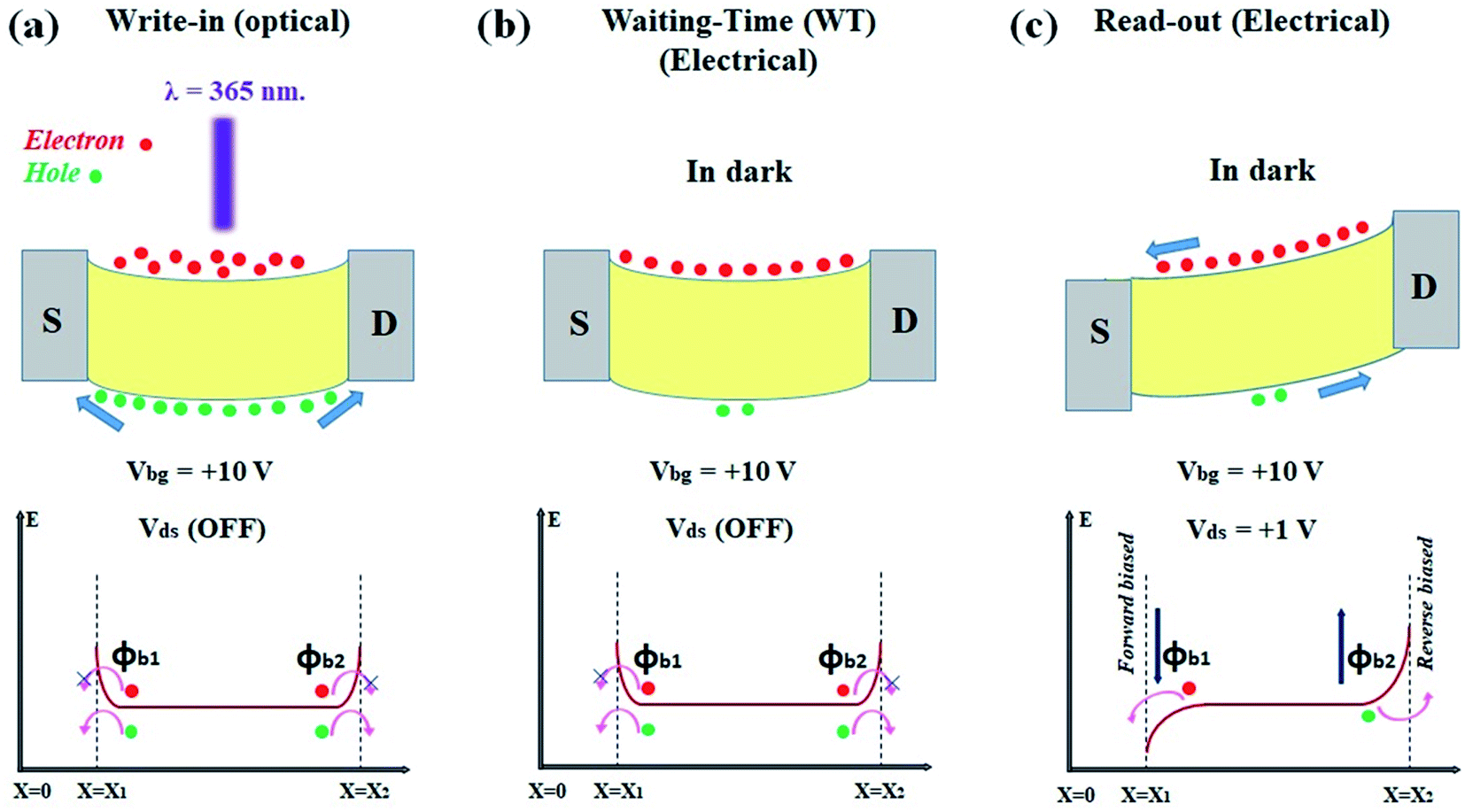 | ||
| Fig. 2 Energy band diagram (with Schottky barrier profile) representing the mechanism of optoelectronic memory process. (a) After UV illumination, trapping of electrons (at the surface of the trapping layer-SiO2) within Schottky barriers (ϕb1 and ϕb2) formed at metal (Pd) and semiconductor interfaces, while holes move through any of the Schottky junction. (b) The electrons remain trapped (due Schottky barriers ϕb1 and ϕb2) over the duration of time termed as waiting time (charge storage time). (c) A read-out bias +1 V (with Vbg = +10 V) leads the Schottky barrier to drop down on one side (ϕb1) releasing the trapped electrons, which is termed as read-out of the information. | ||
The response current inherently depends upon the optical power density (OPD) and exposure dose (ED: exposure duration) of the applied optical wavelength. The WT also has a significant influence on the response (or reading) current. These parameters affecting the reading current are explained in the following section.
To demonstrate the optoelectronics memory process by using a Bi2O2Se-based device, first, the selection of an appropriate optical wavelength was made by measuring the device (under fixed terminal voltage Vds = 1 V, and varying back gate voltage Vbg from −20 V to +40 V) response current in the dark and under exposure to optical wavelengths of 635 nm, 460 nm, and 365 nm as shown in Fig. 3a. The OPD for each wavelength was 1.1 mW cm−2. This measurement shows the optical wavelength of 365 nm (ultraviolet) causes a higher response current. The photo to dark current ratio (PDCR = Iph/Idark, where Iph = Illumination – Idark)62 for wavelengths 635 nm, 460 nm, and 365 nm was 1.579, 2.571, and 4.464, respectively (Fig. S1†). Since the optical wavelength of 365 nm showed the highest PDCR, it can generate an adequate number of photonic charges (e–h pairs), so this UV light was selected for exposure throughout the demonstration of the optoelectronic memory process. Next, the effect of the back gate voltage on the response current for a duration of 10 s was measured (Fig. 3b) for exposure with an OPD of 1.1 mW cm−2 and a duration of 500 ms. The terminal voltage (Vds) was 1 V while the back gate voltage Vbg was selected from 0 V to 40 V. The values applied for the back gate voltage were 0, 5, 10, 15, 20, 25, 30, 40 V, and the corresponding peak values of the response current were 24.3, 27.8, 32.3, 36.4, 39.9, 43.2, 46.5, and 51.9 μA, respectively (Fig. S2†). The measurements show that the effect of the back gate voltage not only increases the peak value of the response current but also improves the decay of the response current over time. The slow decay of the response current indicates the storage of photonically generated charge over more time, which improves the WT of optoelectronic memory. The bolometric effect has been observed with Bi2O2Se due to thermal heat caused by optical incident power.62 This effect is found both with and without back gate voltage. We observed that the photoconductive effect without a back gate voltage shows a current of 250 μA s−1 and a bolometric effect with a current of 6.8 μA s−1, while with a back gate voltage, the photoconductive effect shows a current of 680 μA s−1 and a bolometric effect with a current of 5.4 μA s−1. This shows that the back gate voltage increases the photoconductive effect while slowing the current in the region of the bolometric effect. This is due to leakage of charge causing a gate current when a higher back gate voltage is applied, and hence, the total charge that needs to be contributed to the bolometric effect is reduced, resulting in a slowdown of the current in the region of the bolometric effect (Fig. S3†). The leakage of charge (stored information) in the form of gate current increases with gate voltage at higher values. The leakage of charge needs to be avoided to retain the stored information over time. Fig. S4† shows gate currents of 0.4, 2, 9, 20, 36, 60, 86, and 155 pA with applied back gate voltages of 0, 5, 10, 15, 20, 25, 30, and 40 V. To prevent loss of information and to demonstrate the optical memory process with maximum charge storage (information writing) and minimum charge leakage (information loss), the selected value of the back gate voltage was 10 V. With this value of the back gate voltage, we measured the peak value of charge and then the value of charge after 10 s of decay as shown in Fig. S5.† We observed that the amount of charge with Vbg = 10 V (q ∼ 7.2 × 10⁻⁷ C) was significantly higher than the charge at Vbg = 0 V (q ∼ 5.4 × 10⁻⁷ C). After 10 s, the remaining amount of charge with Vbg = 10 V and 0 V were ∼3.8 × 10⁻⁷ C and ∼1.8 × 10⁻⁷ C, respectively. This inferred that the selection of Vbg = 10 V is pertinent for the demonstration of the optoelectronic memory process. The OPD is one of the responsible parameters for the generation of photonic charge. Fig. S6† shows the amount of photonic charge generated with different levels of OPD. The plot indicates that the amount of photonic charge increases at a much higher rate at initial values of OPD (∼1 mW cm−2), while the incremental rate of photonic charge becomes slower as the OPD increases to higher values (>1.1 mW cm−2). We found an OPD of 1.1 mW cm−2 to be appropriate for exposure by observing the plotted numerical values in Fig. S6.† After observing the effects of OPD, we measured the effect of exposure duration (ED), as shown in Fig. 3c. It was found that as the ED increases, the peak response current also increases.20 As the ED was increased to values of 0, 50, 100, 200, 300, 400, and 500 ms, the response current values were measured to be 8.9, 23, 24.75, 27.55, 29.6, 31.3, and 33.9 μA, respectively. With this measurement, we selected an ED of 500 ms. Fig. S7† shows that the peak amount of photonic charge increases as the exposure dose increases. During the measurement of the effect of ED on the response current (or photonic charge), we also closely observed the dependency of the bolometric effect on ED. Fig. S8† shows that when the ED was 50 ms, the bolometric effect was less significant, and when the ED was increased to 500 ms, the bolometric effect became prominent. This is because more thermal heat caused by boosting the ED leads to the effective appearance of bolometric effects. The WT is another key parameter that governs the performance of optoelectronic memory. To analyze the effect of WT on the response current, we used an exposure by a 365 nm laser with an OPD of 1.1 mW cm−2 and an ED of 500 ms, as these were the preselected parameters. The applied voltages Vds and Vbg were 1 V and 10 V, respectively. Fig. 3d represents the pulses of the output response current having different peak values because they acquired different WTs. This bears out the downward trend of the response current with increasing WT. The major factor responsible for the decay of the peak response current is the leakage of charge through the trapping layer (SiO2) due to the applied back gate voltage. To avoid such leakage of charge, we apply a comparatively lower value of back gate voltage, as discussed earlier (Fig. S4†). More WT causes more leakage of charge that leads to the loss of information. Fig. S9† represents the decay of charge with respect to different WTs. When the WT was small (<1 s), the decay of charge was observed to be slow, and when the WT was increased (>1 s), the charge decayed at a much faster rate. With this measurement, we selected a WT of 500 ms (<1 s) for the demonstration of optoelectronic memory. Furthermore, the variation in the ON/OFF ratio with parameters such as back gate voltage (Vbg), ED, WT, and OPD for the present optoelectronic memory device was determined and is presented in Fig. S10.†
 | ||
| Fig. 3 Bi2O2Se based optoelectronic memory. (a) Variation in device response current in the dark and under exposure with different wavelengths 635 nm, 460 nm, and 365 nm with back gate voltage (applied Vds = +1 V). (b) Effect of back gate voltage (0 V to 40 V) on the response current when using UV exposure (365 nm power density 1.1 mW cm−2, duration 500 ms). (c) The significant effect of exposure dose on the response current. The peak response current increases when exposure dose increases from 0 ms, to 500 ms. (d) The peak response current was observed to decrease while waiting time continues to increase. (e) Write–Wait–Read process for first single pulse application. Write process is done by applying optical pulse (365 nm, power density 1.1 mW cm−2, exposure duration 500 ms) with back gate voltage +10 V. After waiting time of 500 ms, a read out bias +1 V is applied between the source and drain to extract the information as read out current. (f) Six consecutive cycles of Write–Wait–Read (WWR) operation proving the successful realization of optoelectronics memory process. | ||
Fig. 3e represents one complete step of the write–wait–read (WWR) process, elaborating the function of optoelectronic memory. First, an optical pulse was applied as a write-in pulse (λ = 365 nm, OPD = 1.1 mW cm−2, ED = 500 ms). This optical pulse causes the generation of e–h pairs by the active layer, out of which electrons become trapped at the interface of Bi2O2Se/SiO2. After the write-in pulse, a WT of 500 ms was taken into account with Vbg = +10 V and Vds = 0 V. Upon completion of the WT, a read-out bias Vds = +1 V was applied along with Vbg = +10 V. A response current pulse (∼22.5 μA) was measured and regarded as a read-out pulse. It is quite interesting that the duration of the read-out pulse (electrical current) is approximately 500 ms, which is equal to the duration of the applied optical write-in pulse. The output response current decreases and reaches its previous level when Vds reaches 0 V again after a duration of 10 s. To confirm our implementation, we repeated the write–wait–read (WWR) steps six consecutive times (including the first pulse shown in Fig. 3e), as represented in Fig. 3f. The exposure wavelength, OPD, and ED were 365 nm, 1.1 mW cm−2, and 500 ms, respectively, while the write-in bias (Vbg) was +10 V and the read-in bias (Vds) was +1 V. All the associated parameters, including WT (500 ms), were kept invariant for each step of the six consecutive cycles of the WWR process. The read-out current pulse level was observed to be ∼22.5 μA during each step. The consistency in the read-out current level proves the successful realization of the optoelectronic memory function utilizing a Bi2O2Se-based device. After each read-out bias, the output current reverts to its original level (dark current level) by showing some relaxation with little difference each time. This was mainly observed under low current levels. The possible factors for such behavior are excess stored charge22 or substrate surface effects. Although these effects may lead to further studies relating to performance improvement of the device, such effects were observed to be less significant at the peak level of the output response current; hence, we did not pay much attention to such effects quantitatively in our present study. Additionally, we have completed measurements of optoelectronic memory in a dark environment at room temperature while ignoring the other influencing factors of the signal-to-noise (S/N) ratio and the effect of thermal excitations,20 as such effects are more crucial with low current level (pA). A brief comparison with major reported references on optoelectronic memory processes based on 2D materials is presented in Table S1.†
With this demonstration, we successfully realized optoelectronic memory using a Bi2O2Se-based device. Furthermore, making such devices integral parts of an array leads to the development of image sensors in which one device will represent one pixel. Moreover, the ability to gather information from illumination vindicates the application of such Bi2O2Se-based devices in the development of artificial eyes.
Associative learning process
One of the important key aspects of the learning process is conditioned learning, also known as the associative learning process.29–31,69 This conditioned learning process is accomplished using an unconditioned stimulus (US) in association with a neutral stimulus (NS) to alter the behavioral response into a conditioned response (CR). The proposed conditioned learning process is that of a dog drooling when offered a piece of bone as food (Fig. 4b). Before conditioning, the dog drools (unconditioned response- UR) by seeing piece of bone (US) and does not drool (no conditioned response- NCR) by ringing the bell (NS) only. During conditioning, the dog drools (UR) when seeing piece of bone (US) associated with ringing bells (NS). After conditioning, the dog shows drooling (CR) with a ringing bell (CS) only. This infers that the neutral stimulus (ringing bell) shows no conditioned response and has become a conditioned stimulus (CS) showing a conditioned response (CR). An extinction represents the resumption of previous behavior by CS → NS with CR → no response, which is also termed as forgetting. To demonstrate the proposed conditioned learning process, an optical input wavelength of 635 nm was used as neutral stimulus (NS), and 525 nm was used as unconditioned stimulus (US) with the present Bi2O2Se device (Fig. 4a). The optical input pulse period was 500 ms with a power density of 2.0 mW cm−2. The output response current was considered the indicator of behavioral change (of the dog) with a threshold current level of 35 μA for the present device. When the current level is higher than the threshold for any optical input, the dog’s behavior is assumed to be “drooling”, and when the current level is lower than the threshold, the dog’s behavior is assumed to be “no drooling”. Before conditioning, groups of 10 consecutive pulses of wavelength 525 nm were used. It (US) was applied three times, and the output current was 42.6 μA, higher than the threshold level (35 μA), causing an unconditioned response (UR-drooling) (Fig. 4c). Ten consecutive pulses of wavelength 635 nm (NS) were applied three times, and the output current was observed to be 32.5 μA, lower than the threshold level (35 μA), showing no conditioned response (NR-no drooling) (Fig. 4d). During conditioning, the optical wavelength of 525 nm was applied associated with wavelength 635 nm (US + NS) in three groups of 10 consecutive pulses. The output response current was observed to be 47.0 μA, higher than the threshold (35 μA), showing an unconditioned response (UR-drooling) (Fig. 4e). After conditioning, 10 consecutive pulses of wavelength 635 nm were applied three times, and the output current was observed to be 42.1 μA, higher than the threshold level (35 μA), showing a conditioned response (CR-drooling) (Fig. 4f). Hence, the wavelength 635 nm became a conditioned stimuli (CS) that caused no response behavior (no drooling) of the dog to be altered into conditioned response (drooling as conditioned learning). This conditioned response did not remain over a long period of time, and after 90 seconds, an extinction behavior was observed by applying 10 consecutive pulses of 635 nm wavelength three times. The output current was 33.3 μA, lower than the threshold level (35 μA), and thus showed no conditioned response (NR-no drooling). This emulates “forgetting” (Fig. 4g). Therefore, before conditioning, the optical input of 635 nm was a neutral stimulus and became a conditioned stimulus after conditioning (memory). The conditioned stimulus was again converted into neutral stimulus by extinction (forgetting) over a duration of 90 s. The levels of peak currents before conditioning, during conditioning, after conditioning, and extinction are represented in Fig. S11† to show the complete process in one view. Thus, the present device shows the ability to mimic the associative learning process by using all the optical inputs and photoresponse current as output, demonstrating this Bi2O2Se device as an optical neuro device with enough capability to show learning/memory and forgetting processes analogous to the biological neurofunction of the human brain.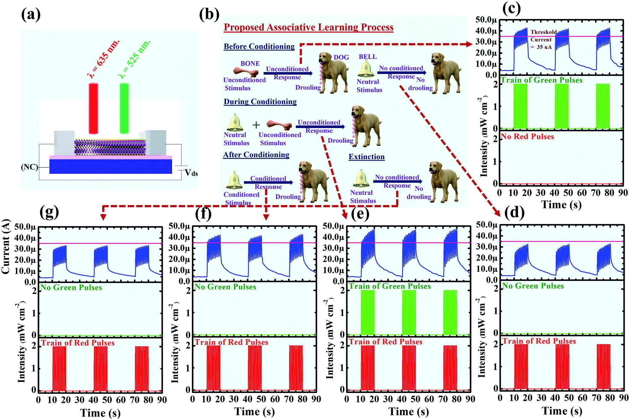 | ||
| Fig. 4 Mimicking associative learning process. (a) Schematic of device structure with exposure of optical wavelengths 525 nm and 635 nm. (b) Proposed associative learning process showing unconditioned and conditioned response (conditioned learning) by the dog followed by extinction (forgetting). (c) Unconditioned response (on application of 525 nm before conditioning). (d) No conditioned response (on application of 635 nm before conditioning). (e) Unconditioned response (on application of 525 nm + 635 nm during conditioning). (f) Conditioned response (on application of 635 nm only after conditioning). (g) Extinction (on application of 635 nm only, after 90 s of conditioning). | ||
Digital logic function
In this section, we demonstrate the realization of the basic logic functions “AND”, “OR”, “NAND” and “NOR” by a similar device, as shown in Fig. 5a.2,16,26–28 The optical input combinations, input-1 (635 nm) and input-2 (525 nm) with an intensity of 2.0 mW cm−2 are regarded as binary inputs (with 525 nm as the most significant bit MSB, and 635 nm as the least significant bit LSB), while the photoresponse current (Iout) is assumed to be the output for “AND” and “OR” logic gates under modulatory back gate voltages (Vbg) of 0 V and 10 V, respectively. The output resistance (Rout) of the device is assumed to be the output for the “NAND” and “NOR” logic gates (with Vbg 0 V and 10 V, respectively). The device characteristics were measured in the dark (with and without back gate voltage, i.e., Vbg) and under exposure to light (with and without Vbg), as shown in Fig. S12.† | ||
| Fig. 5 Realizing the function of digital logic gates. (a) The device under exposure with light 635 nm and 525 nm, as optical binary inputs. (b) Represents device function by logical variation of output current in response of binary optical input combinations for operation of AND gate, and OR gate. (c) Output current level (threshold = 30 μA) reveals AND, and OR logic while the corresponding output resistance (threshold = 3.33 KΩ) shows NAND and NOR logic. | ||
Fig. 5b represents the schematic diagram for the operation of “AND” and “OR” gates. If a particular optical input is “ON”, it represents logical “1”, while optical input “OFF” represents logical “0”. The output represents logical “1” when the output current level (Iout) is higher than (or equal to) the threshold value (Ith = 30 μA) and “0” when Ith > Iout. For the functional realization of the “AND” gate without a back gate voltage (Vbg = 0 V), the applied optical input combinations are “00”, “01”, “10”, and “11”. The output currents measured are 4.6, 26.2, 28.7, and 31.7 μA, which reveal outputs “0”, “0”, “0” and “1”, respectively (Table 1), proving the logic function for the “AND” gate. For the “OR” gate, a modulatory back gate voltage is applied (Vbg = 10 V), which lifts up the current level from 4.6 μA to 9.6 μA. With the same threshold value of output current (Ith = 30 μA) as the “AND” gate, optical input combinations “00”, “01”, “10”, and “11” are applied, and the output currents measured are 9.6, 35, 36.8, and 39 μA, respectively, corresponding to the outputs “0”, “1”, “1” and “1”, respectively (Table 1), proving the logic function for the “OR” gate.
| V bg (V) | Logic operation | Input-2 (λ = 525 nm) green | Input-1 (λ = 635 nm) red | Output photocurrent (μA) | Comparison with threshold current Ith (30 μA) | Corresponding logical output |
|---|---|---|---|---|---|---|
| 0 | AND | 0 | 0 | 4.6 | 4.6 < 30 | 0 |
| 0 | 1 | 26.2 | 26.2 < 30 | 0 | ||
| 1 | 0 | 28.7 | 28.7 < 30 | 0 | ||
| 1 | 1 | 31.7 | 31.7 > 30 | 1 | ||
| 10 | OR | 0 | 0 | 9.6 | 9.6 < 30 | 0 |
| 0 | 1 | 35 | 35 > 30 | 1 | ||
| 1 | 0 | 36.8 | 36.8 > 30 | 1 | ||
| 1 | 1 | 39 | 39 > 30 | 1 |
For the “NAND” and “NOR” gates, shown in Fig. 5c, the device output resistance is regarded as the output for the “NAND” and “NOR” gates. For the “NAND” gate, no modulatory voltage is applied (Vbg = 0 V). The threshold value of the output resistance (Rth) is 3.33 KΩ. If the output resistance for a particular input combination is higher than (or equal to) the threshold value (Rth ≤ Rout), the output is regarded as logical “1”, and if the output resistance is lower than the threshold value (Rth > Rout), the output is regarded as logical “0”. For the “NAND” gate, the measured output resistances for optical input combinations “00”, “01”, “10”, and “11” are 21.74, 3.82, 3.48, and 3.15 KΩ, respectively, corresponding to outputs “1”, “1”, “1”, and “0” (Table 2), proving the realization of the “NAND” gate. For the “NOR” gate, a modulatory back gate voltage is applied (Vbg = 10 V). With the same threshold value of output resistance (Rth = 3.33 KΩ) as the “NAND” gate, optical input combinations “00”, “01”, “10”, and “11” are applied, and the output resistances measured are 10.41, 2.86, 2.72, and 2.56 KΩ, respectively, corresponding to the outputs “1”, “0”, “0” and “0”, respectively (Table 2), showing the logic function of the “NOR” gate.
| V bg (V) | Logic operation | Input-2 (λ = 525 nm) green | Input-1 (λ = 635 nm) red | Output resistance (KΩ) | Comparison with threshold resistance (3.33 KΩ) | Corresponding logical output |
|---|---|---|---|---|---|---|
| 0 | NAND | 0 | 0 | 21.74 | 21.74 > 3.33 | 1 |
| 0 | 1 | 3.82 | 3.82 > 3.33 | 1 | ||
| 1 | 0 | 3.48 | 3.48 > 3.33 | 1 | ||
| 1 | 1 | 3.15 | 3.15 < 3.33 | 0 | ||
| 10 | NOR | 0 | 0 | 10.41 | 10.41 > 3.33 | 1 |
| 0 | 1 | 2.86 | 2.86 < 3.33 | 0 | ||
| 1 | 0 | 2.72 | 2.72 < 3.33 | 0 | ||
| 1 | 1 | 2.56 | 2.56 < 3.33 | 0 |
Therefore, it is clear that the operation of basic logic gates “AND” and “OR” and universal logic gates “NAND” and “NOR” can be realized by tuning optical input combinations and applying modulatory bias. Since the operation of logic gates has been performed independently without reconfiguration of the device structure, this paves the way for such devices to be an integral part of logic circuits embedded within optical integrated chips with ultrahigh speed at low power level. Following similar concepts, the function of other logic gates and complex logic functions can also be realized by proper tuning of optical inputs and appropriate interconnections of such logic circuits.
Binary to decimal converter
In this section, we demonstrate the realization of converting a basic number system, binary to decimal, by employing the same device as in the previous section with an invariant structure. The 4 bit binary-to-decimal converter utilizes precisely tuned four optical inputs (385 nm, 490 nm, 595 nm, 740 nm) combinations (with each OPD of 2.0 mW cm−2) shown in Fig. 6a, considered as four binary inputs with 385 nm at the place of the most significant bit (MSB) and 740 nm at the place of the least significant bit (LSB). The optically induced electrical current output is regarded as equivalent decimal output (with some approximation). The device characteristics were measured in the dark and under exposure to selected wavelengths, as shown in Fig. S13.† | ||
| Fig. 6 Represents realization of binary to decimal conversion. (a) The device under exposure with wavelengths 740 nm, 595 nm, 490 nm, and 385 nm as binary optical inputs. (b) Represents device function by showing variation of output current in response to optical input combinations. (c) Linearity of output response current levels resulted from sequentially applying binary optical input combinations. | ||
Fig. 6b represents the schematic diagram for the operation of the binary-to-decimal converter. A particular optical input represents a binary “1” when it is ON (used for exposure) and a binary “0” when it is OFF (not used for exposure). For binary input “0000”, all the optical inputs were set in the OFF condition, and the output current was measured to be 4.86 μA (same as the dark current level). For binary input “0001”, only wavelength 740 nm was applied for exposure, while other optical inputs remained in the OFF state. The measured output current was 21.89 μA. Next, binary input combination 0010 was applied using a wavelength of 595 nm for exposure, keeping all other wavelengths in the OFF state. The measured output current was 23.94 μA. The third binary input combination, “0011”, was applied using a wavelength of 740 nm and 595 nm for exposure while simultaneously maintaining other wavelengths in the OFF state. The output current was measured as 26.03 μA. Following similar steps to apply optical inputs, all 4 bit binary input combinations from “0000” to “1111” were applied. The output current was measured to be 4.86 μA, 21.89 μA, 23.94 μA, 26.03 μA, 28.30 μA, 30.91 μA, 32.28 μA, 34.43 μA, 36.79 μA, 38.54 μA, 40.83 μA, 42.95 μA, 44.41 μA, 46.97 μA, 48.92 μA, and 50.73 μA, as represented in Table 3. The output current values show upgrading linear behavior (Fig. 6c) by leaving the first value 4.86 μA for input combination “0000”. The increment in output current was almost constant with an incremental difference of approximately 2 μA (with respect to peak values of current). We used an empirically fitted formula, d = (IP – 20)/2 (where “d” is a reduced value with respect to the output peak current IP for each binary optical input combination from “0000” to “1111”). This leads the output values to −7.57, 0.945, 1.97, 3.015, 4.15, 5.455, 6.14, 7.215, 8.395, 9.27, 10.415, 11.46, 12.205, 13.485, 14.46, and 15.365, respectively, as presented in Table 3. To visualize the equivalent decimal number from the output, the following empirically fitted formula was adopted, where “D” represents the equivalent decimal number, and “a” and “b” represent the integer and fractional parts of “d”, respectively.
| D = {0,d < 0} |
| ={a,d = a + b (a = integer part, b = fractional part < 0.555)} |
| ={a + 1, d = a + b (a = integer part, b = fractional part > 0.555)} |
| Input-4 (λ = 385 nm) | Input-3 (λ = 490 nm) | Input-2 (λ = 595 nm) | Input-1 (λ = 740 nm) | Output current level IP (μA) | d = (IP – 20)/2 | D = Positive approximation of “d” |
|---|---|---|---|---|---|---|
| 0 | 0 | 0 | 0 | 4.86 | −7.57 | 0 |
| 0 | 0 | 0 | 1 | 21.89 | 0.945 | 1 |
| 0 | 0 | 1 | 0 | 23.94 | 1.97 | 2 |
| 0 | 0 | 1 | 1 | 26.03 | 3.015 | 3 |
| 0 | 1 | 0 | 0 | 28.30 | 4.15 | 4 |
| 0 | 1 | 0 | 1 | 30.91 | 5.455 | 5 |
| 0 | 1 | 1 | 0 | 32.28 | 6.14 | 6 |
| 0 | 1 | 1 | 1 | 34.43 | 7.215 | 7 |
| 1 | 0 | 0 | 0 | 36.79 | 8.395 | 8 |
| 1 | 0 | 0 | 1 | 38.54 | 9.27 | 9 |
| 1 | 0 | 1 | 0 | 40.83 | 10.415 | 10 |
| 1 | 0 | 1 | 1 | 42.92 | 11.46 | 11 |
| 1 | 1 | 0 | 0 | 44.41 | 12.205 | 12 |
| 1 | 1 | 0 | 1 | 46.97 | 13.485 | 13 |
| 1 | 1 | 1 | 0 | 48.92 | 14.46 | 14 |
| 1 | 1 | 1 | 1 | 50.73 | 15.365 | 15 |
By using this, the equivalent decimal output for input “0000” is “0” (d = −7.57 < 0), for input “0001”, the decimal output is “1” (d = 0.945 = 0 + 0.945 > 0.555, D = a + 1 = 0 + 1 = 1), for input “0010”, the decimal output is “2” (d = 1.97 = 1 + 0.97 > 0.555, D = a + 1 = 1 + 1 = 2), and for the following input combinations, the equivalent decimal output D = “a” (as fractional part < 0.555). This leads to decimal values of 0, 1, 2, 3, 4, 5, 6, 7, 8, 9, 10, 11, 12, 13, 14, and 15, resulting from peak values of the output current corresponding to binary inputs from 0000 to 1111 (Table 3).
Therefore, the operation of a 4 bit binary-to-decimal converter has been demonstrated with the help of four different optical wavelengths that were precisely tuned to modulate the output current. This demonstration is a remarkable sign of the realization of interconversion among different number systems that can be applied for advanced computing.
Experimental section
Synthesis of Bi2O2Se nanoplates over MICA substrate
A quartz tube (diameter = 3 inches) and an in-built LPCVD system composed of three different heating zones, T-1 (downstream), T-2 (middle), and T-3 (upstream), was adopted for the synthesis of Bi2O2Se nanoplates. MICA as a suitable substrate was placed at the heating zone T-1, while precursors Bi2O3 and Bi2Se3 were placed at heating zones T-2 and T-3, respectively. To evacuate oxygen from the tube, a flow of Ar was used. The emblematic growth time was 40 min, with temperature conditions of 500 °C, 700 °C, and 500 °C for substrate (T-1), Bi2O3 (T-2), and Bi2Se3 (T-3), respectively, whereas the tube pressure was 100 torr and the flow rate of the carrier gas (Ar) was 200 sccm.Material characterization
To capture optical microscopy (OM) images of Bi2O2Se nanoplates, an optical microscope (OLYMPUS BX53 M) was used. The thickness of Bi2O2Se nanoplates was measured by atomic force microscopy (AFM B067, Bruker Corp.). Raman spectroscopy of the samples was carried out under excitation at 532 nm laser with a 100× objective lens (UniDRON, CI Technology). The dimensions and elemental composition of Bi2O2Se nanoplates were determined via FESEM analysis (JOEL JSM-7500F, accelerating voltage: 10 kV. Resolution: 1 nm) and EDS analysis (OXFORD INCA X-ACT), respectively. The cross-sectional HRTEM image of Bi2O2Se was obtained via a focused-ion beam in a dual-beam microscope (JEM-2100F, acceleration voltage 200 kV).Transferring Bi2O2Se nanoplates from MICA to SiO2 substrate
MICA (having as-grown Bi2O2Se nanoplates) is first spin coated by PMMA in two steps (step-1: 500 rpm for 7 s, step-2: 2000 rpm for 60 s), then baked (150 °C, for 1 min) to improve the adhesion of PMMA with Bi2O2Se. A PDMS sheet of sufficient dimension was attached over the PMMA spin-coated substrate and baked again (150 °C for 2 min) for better adhesion of the PDMS sheet. Cooling of the sample was done with a flow of N2. Next, water was used to separate the PDMS sheet from MICA by dipping the substrate in water for a sufficient period (∼5 min). Due to good adhesion, Bi2O2Se nanoplates remain attached to the PDMS sheet via the PMMA layer. This PDMS sheet was attached over fresh Si substrate (SiO2/Si), baked (150 °C, for 2 min), and then cooled by N2. Acetone treatment helps to detach the PDMS sheet, leaving Bi2O2Se nanoplates over the SiO2/Si substrate. Bi2O2Se/SiO2/Si was treated many times with acetone/IPA to avoid the PMMA residue. The minimum PMMA residue was observed with samples kept in acetone overnight.Device fabrication
For the fabrication of the device, an LED lithography system was used to define a 2-terminal pattern for metal contact by spin coating with PR AZ5214E in two steps (step-1: 700 rpm for 5 s, step-2: 4000 rpm for 60 s) followed by baking at 90 °C for 90 s. After exposure, an MIF-300 developer was used to develop the pattern (developer time was 4 s, water treatment was 20 s). The metal Pd (50 nm) was deposited by a thermal evaporator. Liftoff yields the two terminal patterns. Aluminum (Al, 3000 nm) was deposited to make the back contact using a thermal evaporator again.Measurements
For both optical and electrical measurements simultaneously, a CoolLED pE-400 monochromatic light source (λ = 365 nm–770 nm) was used with a semiconductor device analyzer B1500A. A NOVA II power meter (OPHIR Photonics) was utilized to measure the OPD (mW cm−2). All measurements were completed in a sufficiently dark environment at room temperature.Conclusion
In summary, we have demonstrated that a single Bi2O2Se-based structure shows versatility for multiple optoelectronic applications. The device performed the function of optoelectronic memory, starting with a write-in process done by trapping electrons generated by UV exposure, followed by achieving WT and read-out (detrapping of electrons) by means of electrical energy. Furthermore, an associative learning process was demonstrated, controlled by a 635 nm optical wavelength (NS) and a 525 nm wavelength (US). The variation in the output current along the threshold level was used to discriminate the behavior (CR/UR). The same optical wavelengths are regarded as binary inputs to realize the operation of digital logic “AND”, “OR”, “NAND” and “NOR” gates. With the help of universal logic gates, the functions of other digital logic can be realized, creating a path for the development of low-power opto-digital logic devices. Moreover, four dissimilar wavelengths were observed: 740 nm, 595 nm, 490 nm, and 385 nm are precisely tuned and considered binary inputs for the implementation of a 4 bit binary to the decimal converter in which the value of the output current represents the equivalent decimal output. Our study elucidates the light sensing property of Bi2O2Se, making it a promising material for the development of in-computing optoelectronic memory, image sensor, and artificial intelligence.Author contributions
Dharmendra Verma: conceptualization, data curation, investigation, methodology, writing – original draft. Bo Liu: validation, visualization, writing – review & editing. Tsung-Cheng Chen: validation, visualization, writing – review & editing. Lain-Jong Li: validation, writing – review & editing. Chao-Sung Lai: conceptualization, methodology, resources, validation, funding acquisition, project administration, supervision, writing – review & editing.Conflicts of interest
The authors declare no conflict of interest.Acknowledgements
The present study was supported by grants from the Ministry of Science and Technology (MOST), Taiwan (MOST 109-2221-E-182-013-MY3, MOST 110-2622-8-182-001-TS1) and Chang Gung Memorial Hospital, Taiwan (CMRPD2K0171).References
- H. Tan, G. Liu, X. Zhu, H. Yang, B. Chen, X. Chen, J. Shang, W. D. Lu, Y. Wu and R.-W. Li, Adv. Mater., 2015, 27, 1500039 Search PubMed.
- F. Zhou, Y. Liu, X. Shen, M. Wang, F. Yuan and Y. Chai, Adv. Funct. Mater., 2018, 28, 1800080 CrossRef.
- T. Leydecker, M. Herder, E. Pavlica, G. Bratina, S. Hecht, E. Orgiu and P. Samorì, Nat. Nanotechnol., 2016, 11, 769 CrossRef CAS PubMed.
- J. Cheng, C. Wang, X. Zou and L. Liao, Adv. Opt. Mater., 2018, 7, 1800441 CrossRef.
- F. Zhou, J. Chen, X. Tao, X. Wang and Y. Chai, Research, 2019, 9490413 CAS.
- Z. Sun, J. Li, C. Liu, S. Yang and F. Yan, Nano Lett., 2021, 21, 723 CrossRef CAS PubMed.
- T. Uda, A. Ishii and Y. K. Kato, ACS Photonics, 2018, 5, 559 CrossRef CAS.
- J. Zhao, Z. Wei, X. Yang, G. Zhang and Z. Wang, Nano Energy, 2020, 82, 105692 CrossRef.
- C.-C. Shih, Y.-C. Chiang, H.-C. Hsieh, Y.-C. Lin and W.-C. Chen, ACS Appl. Mater. Interfaces, 2019, 11, 42429 CrossRef CAS PubMed.
- Y.-C. Chiang, C.-C. Hung, Y.-C. Lin, Y.-C. Chiu, T. Isono, T. Satoh and W.-C. Chen, Adv. Mater., 2020, 32, 2002638 CrossRef CAS PubMed.
- X. Zhao, S.-Y. Wei, X.-H. Wang and L.-Z. Qiu, Adv. Opt. Mater., 2021, 9, 2002256 CrossRef CAS.
- C. Gao, H. Yang, E. Li, Y. Yan, L. He, H. Chen, Z. Lin and T. Guo, ACS Photonics, 2021, 8, 3094 CrossRef CAS.
- L. Hu, J. Yuan, Y. Ren, Y. Wang, J.-Q. Yang, Y. Zhou, Y.-J. Zeng and S.-T. Han, Adv. Mater., 2018, 30, 1801232 CrossRef PubMed.
- M. D. Tran, H. Kim, J. S. Kim, M. H. Doan, T. K. Chau, Q. A. Vu, J.-H. Kim and Y. H. Lee, Adv. Mater., 2018, 31, 1807075 CrossRef PubMed.
- F. Gao, X. Zhang, B. Tan, S. Zhang, J. Zhang, D. Jia, Y. Zhou and P. A. Hu, Small, 2021, 17, 2104459 CrossRef CAS PubMed.
- Z. Cheng, C. Ríos, N. Youngblood, C. D. Wright, W. H. P. Pernice and H. Bhaskaran, Adv. Mater., 2018, 30, 1802435 CrossRef PubMed.
- I. Vassalini, I. Alessandri and D. Ceglia, Materials, 2021, 14, 3396 CrossRef CAS PubMed.
- M. S. Choi, G.-H. Lee, Y.-J. Yu, D.-Y. Lee, S. H. Lee, P. Kim, J. Hone and W. J. Yoo, Nat. Commun., 2013, 4, 1 Search PubMed.
- D. Lee, E. Hwang, Y. Lee, Y. Choi, J. S. Kim, S. Lee and J. H. Cho, Adv. Mater., 2016, 28, 1603571 Search PubMed.
- S. Lei, F. Wen, B. Li, Q. Wang, Y. Huang, Y. Gong, Y. He, P. Dong, J. Bellah, A. George, L. Ge, J. Lou, N. J. Halas, R. Vajtai and P. M. Ajayan, Nano Lett., 2015, 15, 259 CrossRef CAS PubMed.
- K. Roy, M. Padmanabhan, S. Goswami, T. P. Sai, G. Ramalingam, S. Raghavan and A. Ghosh, Nat. Nanotechnol., 2013, 8, 826 CrossRef CAS PubMed.
- J. Lee, S. Pak, Y.-W. Lee, Y. Cho, J. Hong, P. Giraud, H. S. Shin, S. M. Morris, J. I. Sohn, S. N. Cha and J. M. Kim, Nat. Commun., 2013, 8, 14734 CrossRef PubMed.
- A. Lipatov, N. S. Vorobeva, T. Li, A. Gruverman and A. Sinitskii, Adv. Electron. Mater., 2021, 7, 2001223 CrossRef CAS.
- Y. Chen, J. Yu, F. Zhuge, Y. He, Q. Zhang, S. Yu, K. Liu, L. Li and Y. M. T. Zhai, Mater. Horiz., 2020, 7, 1331 RSC.
- K. Wang, J. Chen and X. Yan, Nano Energy, 2021, 79, 105453 CrossRef CAS.
- J. Zhao, Z. Zhou, H. Wang, J. Wang, W. Hao, D. Ren, R. Guo, J. Chen, B. Liu and X. Yan, Appl. Phys. Lett., 2019, 115, 153504 CrossRef.
- H. Chen, X. Xue, C. Liu, J. Fang, Z. Wang, J. Wang, D. W. Zhang, W. Hu and P. Zhou, Nat. Electron., 2021, 4, 399 CrossRef CAS.
- K. Zhang, D. Meng, F. Bai, J. Zhai and Z. L. Wang, Adv. Funct. Mater., 2020, 30, 2002945 CrossRef CAS.
- M. Pedroa, J. M. Martineza, R. Rodrigueza, M. B. Gonzalezb, F. Campabadalb and M. Nafriaa, Microelectron. Eng., 2019, 215, 111024 CrossRef.
- M. Yan, Q. Zhu, S. Wang, Y. Ren, G. Feng, L. Liu, H. Peng, Y. He, J. Wang, P. Zhou, X. Meng, X. Tang, J. Chu, B. Dkhil, B. Tian and C. Duan, Adv. Electron. Mater., 2021, 7, 2001276 CrossRef CAS.
- Y. Pei, Z. Zhou, A. P. Chen, J. Chen and X. Yan, Nanoscale, 2020, 12, 13531 RSC.
- A. Emboras, A. Alabastri, P. Lehmann, K. Portner, C. Weilenmann, P. Ma, B. Cheng, M. Lewerenz, E. Passerini, U. Koch, J. Aeschlimann, F. Ducry, J. Leuthold and M. Luisier, Appl. Phys. Lett., 2020, 117, 230502 CrossRef CAS.
- J.-Y. Mao, L. Zhou, X. Zhu, Y. Zhou and S.-T. Han, Adv. Optical Mater., 2019, 7, 1900766 CrossRef CAS.
- Y. Wang, L. Yin, W. Huang, Y. Li, S. Huang, Y. Zhu, D. Yang and X. Pi, Adv. Intell. Syst., 2021, 3, 2000099 CrossRef.
- J. Wu, C. Tan, Z. Tan, Y. Liu, J. Yin, W. Dang, M. Wang and H. Peng, Nano Lett., 2017, 17, 3021 CrossRef CAS PubMed.
- H. Fu, J. Wu, H. Peng and B. Yan, Phys. Rev. B, 2018, 97, 241203 CrossRef CAS.
- J. Wu, Y. Liu, Z. Tan, C. Tan, J. Yin, T. Li, T. Tu and H. Peng, Adv. Mater., 2017, 29, 1704060 CrossRef PubMed.
- J. Wu, C. Tan, Z. Tan, Y. Liu, J. Yin, W. Dang, M. Wang and H. Peng, Nano Lett., 2017, 17, 3021 CrossRef CAS PubMed.
- T. Ghosh, M. Samanta, A. Vasdev, K. Dolui, J. Ghatak, T. Das, G. Sheet and K. Biswas, Nano Lett., 2019, 19, 5703 CrossRef CAS PubMed.
- Y. Liang, Y. Chen, Y. Sun, S. Xu, J. Wu, C. Tan, X. Xu, H. Yuan, L. Yang, Y. Chen, P. Gao, J. Guo and H. Peng, Adv. Mater., 2019, 31, 1901964 CrossRef PubMed.
- M.-Q. Li, L.-Y. Dang, G.-G. Wang, F. Li, M. Han, Z.-P. Wu, G.-Z. Li, Z. Liu and J.-C. Han, Adv. Mater. Technol., 2020, 5, 2000180 CrossRef CAS.
- Y. Sun, S. Ye, J. Zhang, J. Song, F. Zhou and J. Qu, J. Mater. Chem. C, 2020, 8, 14711 RSC.
- C. Zhang, J. Wu, Y. Sun, C. Tan, T. Li, T. Tu, Y. Zhang, Y. Liang, X. Zhou, P. Gao and H. Peng, J. Am. Chem. Soc., 2020, 142, 2726 CrossRef CAS PubMed.
- M. Kang, H.-J. Chai, H. B. Jeong, C. Park, I.-Y. Jung, E. Park, M. M. Çiçek, I. Lee, B.-S. Bae, E. Durgun, J. Y. Kwak, S. Song, S.-Y. Choi, H. Y. Jeong and K. Kang, ACS Nano, 2021, 15, 8715 CrossRef CAS PubMed.
- U. Khan, Y. Luo, L. Tang, C. Teng, J. Liu, B. Liu and H.-M. Cheng, Adv. Funct. Mater., 2019, 29, 1807979 CrossRef.
- T. Selvamani, S. Anandan, L. Granone, D. W. Bahnemann and M. Ashokkumar, Mater. Chem. Front., 2018, 2, 1664 RSC.
- C. Tan, M. Tang, J. Wu, Y. Liu, T. Li, Y. Liang, B. Deng, Z. Tan, T. Tu, Y. Zhang, C. Liu, J.-H. Chen, Y. Wang and H. Peng, Nano Lett., 2019, 19, 2148 CrossRef CAS PubMed.
- M. Wu and X. C. Zeng, Nano Lett., 2017, 17, 6309 CrossRef CAS PubMed.
- H. Yang, C. Tan, C. Deng, R. Zhang, X. Zheng, X. Zhang, Y. Hu, X. Guo, G. Wang, T. Jiang, Y. Zhang, G. Peng, H. Peng, X. Zhang and S. Qin, Small, 2019, 15, 1904482 CrossRef CAS PubMed.
- A. L. J. Pereira, D. Santamaría-Pérez, J. Ruiz-Fuertes, F. J. Manjón, V. P. Cuenca-Gotor, R. Vilaplana, O. Gomis, C. Popescu, A. Muñoz, P. Rodríguez-Hernández, A. Segura, L. Gracia, A. Beltrán, P. Ruleova, C. Drasar and J. A. Sans, J. Phys. Chem. C, 2018, 122, 8853 CrossRef CAS.
- Q. Fu, C. Zhu, X. Zhao, X. Wang, A. Chaturvedi, C. Zhu, X. Wang, Q. Zeng, J. Zhou, F. Liu, B. K. Tay, H. Zhang, S. J. Pennycook and Z. Liu, Adv. Mater., 2018, 31, 1804945 CrossRef PubMed.
- J. Wu, C. Qiu, H. Fu, S. Chen, C. Zhang, Z. Dou, C. Tan, T. Tu, T. Li, Y. Zhang, Z. Zhang, L.-M. Peng, P. Gao, B. Yan and H. Peng, Nano Lett., 2019, 19, 197 CrossRef CAS PubMed.
- J. Li, Z. Wang, Y. Wen, J. Chu, L. Yin, R. Cheng, L. Lei, P. He, C. Jiang, L. Feng and J. He, Adv. Funct. Mater., 2018, 28, 1706437 CrossRef.
- J. Yang, R. Quhe, Q. Li, S. Liu, L. Xu, Y. Pan, H. Zhang, X. Zhang, J. Li, J. Yan, B. Shi, H. Pang, L. Xu, Z. Zhang, J. Lu and J. Yang, Adv. Electron. Mater., 2019, 5, 1800720 CrossRef.
- R. Quhe, J. Liu, J. Wu, J. Yang, Y. Wang, Q. Li, T. Li, Y. Guo, J. Yang, H. Peng, M. Lei and J. Lu, Nanoscale, 2019, 11, 532 RSC.
- C. Huang and H. Yu, ACS Appl. Mater. Interfaces, 2020, 12, 19643 CrossRef CAS PubMed.
- Y. Chen, W. Ma, C. Tan, M. Luo, W. Zhou, N. Yao, H. Wang, L. Zhang, T. Xu, T. Tong, Y. Zhou, Y. Xu, C. Yu, C. Shan, H. Peng, F. Yue, P. Wang, Z. Huang and W. Hu, Adv. Funct. Mater., 2021, 31, 2009554 CrossRef CAS.
- J.-M. Yan, J.-S. Ying, M.-Y. Yan, Z.-C. Wang, S.-S. Li, T.-W. Chen, G.-Y. Gao, F. Liao, H.-S. Luo, T. Zhang, Y. Chai and R.-K. Zheng, Adv. Funct. Mater., 2021, 31, 2103982 CrossRef CAS.
- B. Liu, Y. Zhao, D. Verma, L. A. Wang, H. Liang, H. Zhu, L.-J. Li, T.-H. Hou and C.-S. Lai, ACS Appl. Mater. Interfaces, 2021, 13, 15391 CrossRef CAS PubMed.
- J. Wu, H. Yuan, M. Meng, C. Chen, Y. Sun, Z. Chen, W. Dang, C. Tan, Y. Liu, J. Yin, Y. Zhou, S. Huang, H. Q. Xu, Y. Cui, H. Y. Hwang, Z. Liu, Y. Chen, B. Yan and H. Peng, Nat. Nanotechnol., 2017, 12, 530 CrossRef CAS PubMed.
- C. Tan, S. Xu, Z. Tan, L. Sun, J. Wu, T. Li and H. Peng, InfoMat, 2019, 1, 390 CrossRef CAS.
- C.-M. Yang, T.-C. Chen, D. Verma, L.-J. Li, B. Liu, W.-H. Chang and C.-S. Lai, Adv. Funct. Mater., 2020, 30, 2001598 CrossRef CAS.
- M. Yu, C. Fang, J. Han, W. Liu, S. Gao and K. Huang, ACS Appl. Mater. Interfaces, 2022, 14, 13507 CrossRef CAS PubMed.
- S. Yang, P. Luo, F. Wang, T. Liu, Y. Zhao, Y. Ma, H. Li and T. Zhai, Small, 2022, 18, 2105211 CrossRef CAS PubMed.
- S. Liu, D. He, C. Tan, S. Fu, X. Han, M. Huang, Q. Miao, X. Zhang, Y. Wang, H. Peng and H. Zhao, Small, 2022, 18, 2106078 CrossRef CAS PubMed.
- C. Fan, B. Dai, H. Liang, X. Xu, Z. Qi, H. Jiang, H. Duan and Q. Zhang, Adv. Funct. Mater., 2021, 31, 2010263 CrossRef CAS.
- W. Chen, U. Khan, S. Feng, B. Ding, X. Xu and B. Liu, Adv. Funct. Mater., 2020, 30, 2004960 CrossRef CAS , (Ref. added in manuscript with no. = 20).
- Y. Guo, X. Wei, J. Shu, B. Liu, J. Yin, C. Guan, Y. Han, S. Gao and Q. Chen, Appl. Phys. Lett., 2015, 106, 103109 CrossRef.
- M. S. Fanselow and A. M. Poulos, Annu. Rev. Psychol., 2005, 56, 207 CrossRef PubMed.
Footnote |
| † Electronic supplementary information (ESI) available. See https://doi.org/10.1039/d2na00245k |
| This journal is © The Royal Society of Chemistry 2022 |