
 Open Access Article
 This Open Access Article is licensed under a Creative Commons Attribution-Non Commercial 3.0 Unported Licence
Ice-assisted electron-beam lithography for MoS2 transistors with extremely low-energy electrons
Guangnan
Yao
abc,
Ding
Zhao
 *bc,
Yu
Hong
a,
Rui
Zheng
bc and
Min
Qiu
*bc
*bc,
Yu
Hong
a,
Rui
Zheng
bc and
Min
Qiu
*bc
aCollege of Optical Science and Engineering, Zhejiang University, Hangzhou 310027, China
bKey Laboratory of 3D Micro/Nano Fabrication and Characterization of Zhejiang Province, School of Engineering, Westlake University, Hangzhou 310024, China. E-mail: zhaoding@westlake.edu.cn
cInstitute of Advanced Technology, Westlake Institute for Advanced Study, Hangzhou 310024, China. E-mail: qiu_lab@westlake.edu.cn
First published on 16th May 2022
Abstract
Ice-assisted electron-beam lithography (iEBL) by patterning ice with a focused electron-beam has emerged as a green nanofabrication technique for building nanostructures on diverse substrates. However, materials like atomically thin molybdenum disulfide (MoS2), can be easily damaged by electron irradiation. To ensure the performance of devices based on sensitive materials, it is critical to control electron-beam induced radiolysis in iEBL processes. In this paper, we demonstrate that electron-beam patterning with extremely low-energy electrons followed by a heating process can significantly reduce the damage to substrate materials. A thin film of water ice not only acts as a sacrificial layer for patterning but also becomes a protecting layer for the underlying materials. As a result, MoS2 field effect transistors with back-gate configuration and ohmic contacts have been successfully fabricated. Moreover, the presence or absence of such a protecting layer can lead to the retention or destruction of the underlying MoS2, which provides a flexible method for creating electrical insulation or connection on 2D materials.
Top-down approaches such as electron-beam lithography (EBL),1–3 photolithography,4 and scanning probe lithography5 have been widely used in the fabrication of micro/nano optoelectronic devices. However, these conventional techniques are facing challenges in processing sensitive materials. For instance, it is inevitable for them to develop chemical resists in solvents, which would result in dissolution of certain materials, e.g. perovskites.6 Besides, high-energy electron irradiation can affect the intrinsic properties of 2D materials,7–9 perovskites10 and metal–organic frameworks,11 thus it is always tricky for EBL to produce devices based on those materials. Recently, a dry mask lamination process called van der Waals stencil lithography has been developed for fabricating 2D transistors.12 However, special attention should be paid to the preparation and positioning of a transferable mask in this method, which requires more fabrication steps compared with a standard lithographic procedure.
Ice-assisted electron-beam lithography (iEBL), also known as ice lithography, has emerged with advantages in nanofabrication, including streamlined workflow, in situ alignment, and full compatibility with non-flat substrates.13–15 Particularly, iEBL can completely avoid the use of solvents,16 which is essential for dealing with sensitive materials. Moreover, electron-beam (e-beam) induced effects including radiolysis, knock-on displacement, heating and electrostatic charging, have been investigated in transmission electron microscopy.17–19 In a scanning electron microscope (SEM), primary beam energy is commonly below 30 keV, leading to neglectable knock-on displacement. Other effects such as heating and electrostatic charging could be reduced by decreasing beam current. Hence, damage to the sample in iEBL is mainly due to e-beam induced radiolysis. It has been shown that free radicals are generated during electrons interacting with ice, which may probably oxidize the sample covered by the ice.20
To relieve the damage caused by e-beam irradiation, here we employ a focused e-beam with extremely low energy (1 keV or less) for patterning the water ice resist. The nanofabrication process was carried out in a commercial SEM integrated with a customized metallization system.21,22 Monolayer MoS2 flakes were purchased from 6Carbon Technology (Shenzhen, China). They were grown onto a Si substrate with an oxide layer of 300 nm by chemical vapor deposition (CVD). As shown in Fig. 1, the whole process includes 6 main steps: cooling, condensing, patterning, heating, metallization and peel-off. Most of these steps have been reported in our previous work except following details.15,23 Firstly, the ice resist is spatially divided into a sacrificial layer and protecting layer (Fig. 1b). During e-beam exposure, patterns are generated in the sacrificial layer and around 100 nm-thick ice in situ remains to protect the underlying MoS2 (Fig. 1c). Meanwhile, the energy of the primary e-beam is 0.3 keV in order to minimize penetration depth of electrons. As a result, scattered electrons could barely go through the protecting layer and reach the underlying MoS2. Secondly, a controllable heating process is adopted to remove the protecting layer before metal deposition (Fig. 1d). Here, the substrate is heated to 160 K, leading to sublimation of ice at a rate of several nanometres per minute. The ice pattern would be slightly broadened due to the heating effect. Finally, all of ice sublimates at room temperature in a vacuum, and the metal film on ice lands on the sample, which can be easily taped for peel-off from the sample surface.
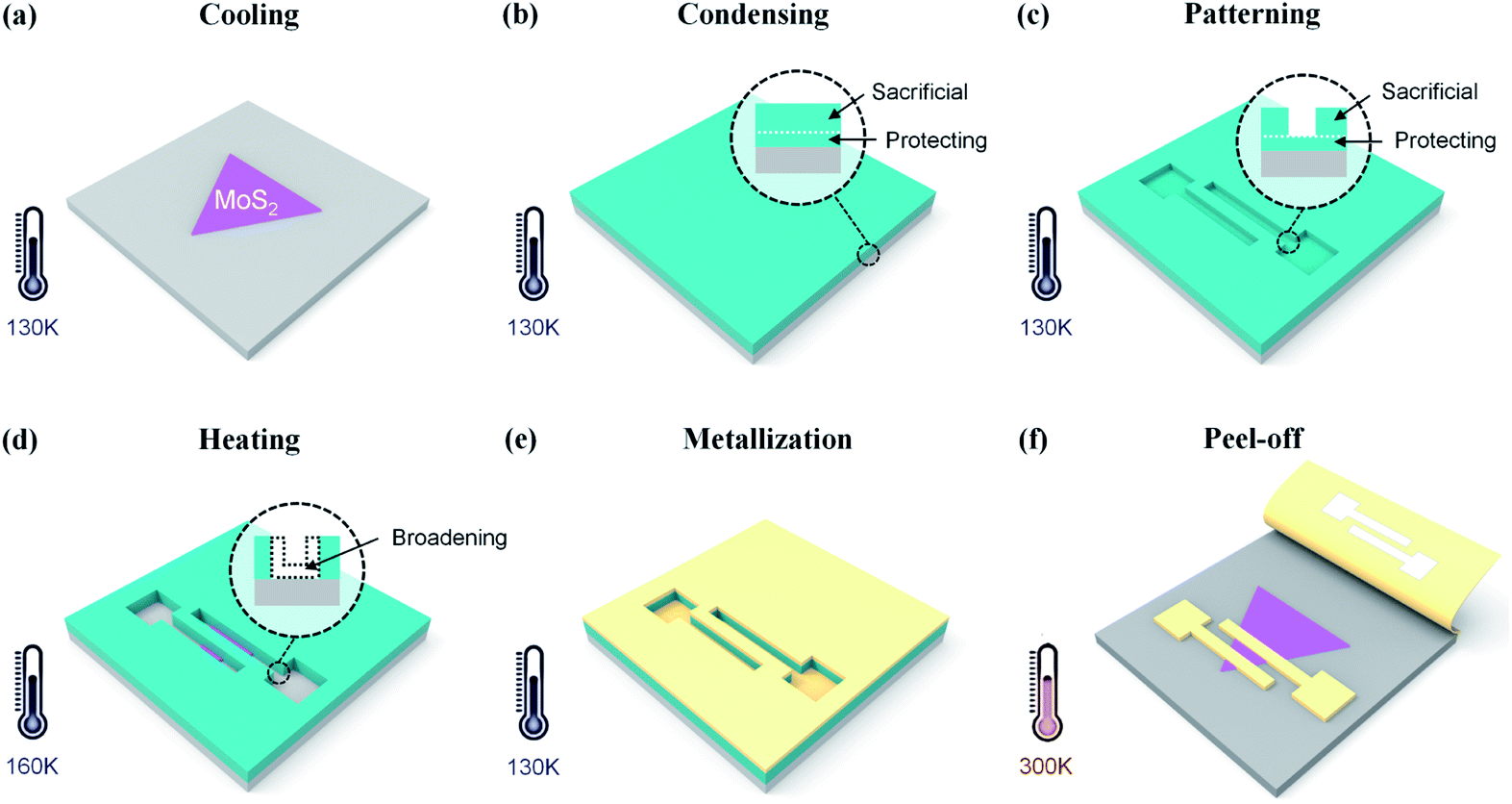 | ||
| Fig. 1 Process flow of iEBL with an in situ formed protecting layer. (a) Cooling: sample stage is cooled down to 130 K. (b) Condensing: a thin ice film is vapor-deposited onto the sample. (c) Patterning: the ice is partly eliminated through low-energy electron irradiation and about 100 nm-thick ice (as a protecting layer during e-beam exposure) remains. (d) Heating: the temperature of sample stage is raised to 160 K and the protecting layer sublimates with the broadening of the ice pattern. (e) Metallization: a metal film is deposited onto the sample. (f) Peel-off: the sample is heated to room temperature and residual metal can be removed by direct peel-off. | ||
In conventional EBL, e-beam exposure at low electron energies (∼1–2 keV) has shown advantages of reduced charging effect, decreased radiation damage and improved throughput.24,25 Nevertheless, low-energy EBL is not expected for high-resolution patterning due to the poor quality of e-beam focusing. It can lead to an enlarged spot size and probably affect the broadening of the linewidth.26–28 In iEBL, our preliminary experiment shows that sub-20 nm-wide lines could be patterned in the ice even at 0.3 keV, which are comparable to those obtained at 20 keV. It indicates that the resolution of iEBL is not appreciably affected by the electron energy. More importantly, primary beam energy in conventional EBL is expected to be no less than 1 keV, otherwise the electrons could not pass through the whole resist layer and a part of the resist remains after development. This means that electrons with a certain energy cannot fully expose a resist with thickness beyond electron penetration depth, i.e., the electron energy restricts the resist thickness. In contrast, the exposure of ice is independent of the electron energy. It is based on the fact that solid ice gradually turns into gaseous products from the surface to the underlying under e-beam irradiation. Therefore, a thick ice layer can be completely removed even using low-energy electrons, such as 0.3 keV in our experiments.
As a demonstration of our low-energy lithography, we have fabricated back-gate field effect transistors (FETs) based on monolayer MoS2. As depicted in Fig. 2a, Au/Ti (30/10 nm) microelectrodes are defined upon monolayer MoS2 on a SiO2/Si substrate. Fig. 2b shows the room-temperature transition curves at different back-gate voltages Vbg ranging from 0 to 30 V. The linear relationship between drain-source current Ids and voltage Vds indicates the formation of ohmic contacts at the metal–semiconductor interface. For comparison, we fabricate another device with the same structure by removing the ice layer entirely using a 1 keV e-beam (Fig. 2c). Not surprisingly, the underlying MoS2 is destroyed due to e-beam irradiation without a protective process. The drain-source current is only a few femtoamperes, of the same order of magnitude as the back-gate current. These results show that destruction or retention of the underlying monolayer MoS2 could be determined by matching primary beam energy (corresponding to electron penetration depth) to ice thickness. Therefore, we can easily create either insulation or connection on 2D materials (Fig. 2d and f) just by regulating the electron energy, which is undoubtedly beneficial to the development of a flexible and efficient fabrication technique towards 2D optoelectronic devices.
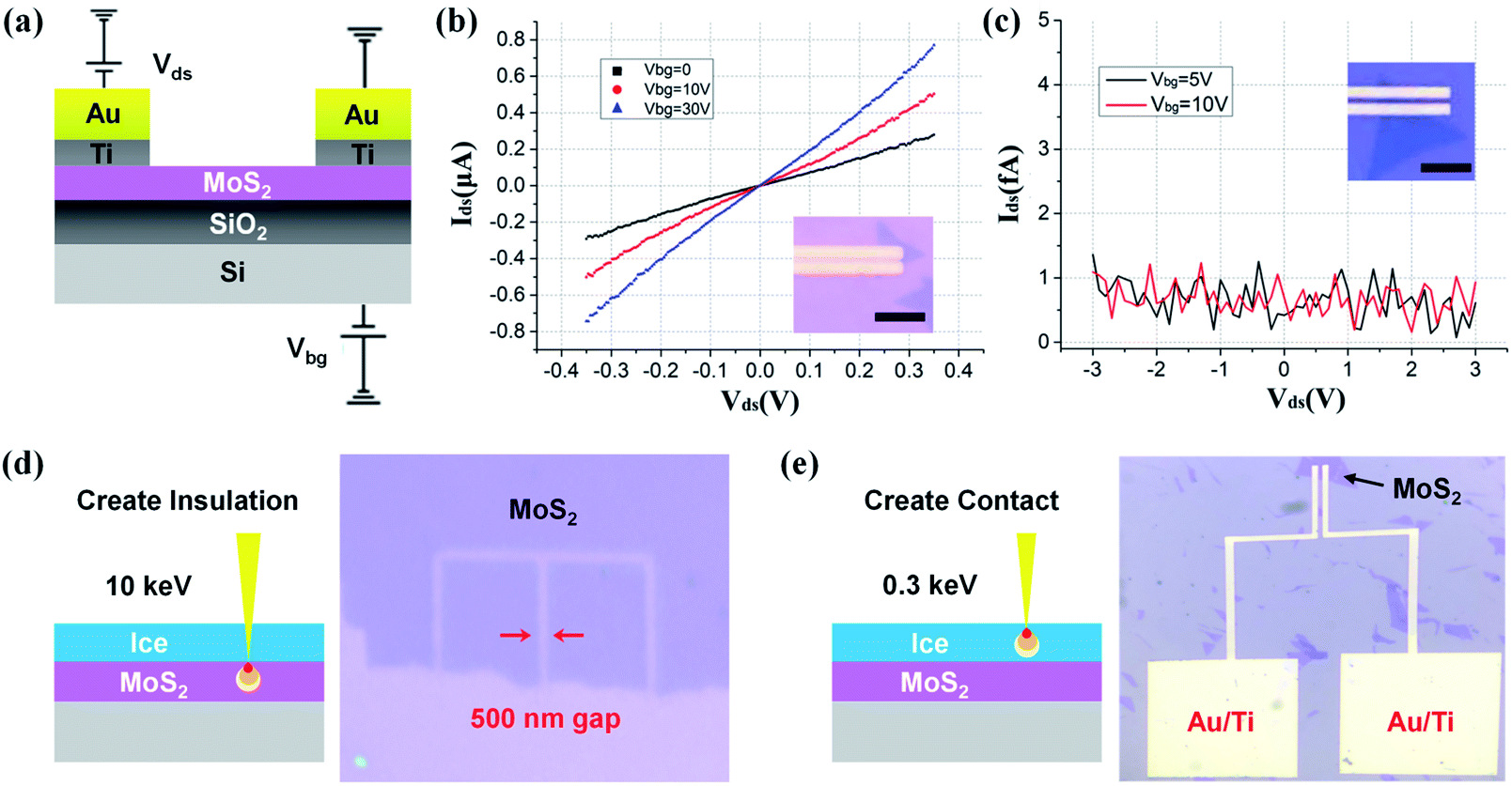 | ||
| Fig. 2 Back-gate FETs based on CVD-grown monolayer MoS2 flakes. (a) Schematic cross section and electrical connections of a back-gate FET. It comprises a silicon substrate as a back-gate electrode and 285 nm-thick SiO2 as a dielectric layer. (b) Ids–Vds curves at different back-gate voltages. The inset is an optical image of the FET. (c) Transition curves of a device fabricated without a protective process. (d and e) Create insulation or connection according to primary beam energy. High energy like 10 keV leads to the destruction of MoS2, while low energy like 0.3 eV is beneficial to a good electrical connection. Scale bars are 10 μm. | ||
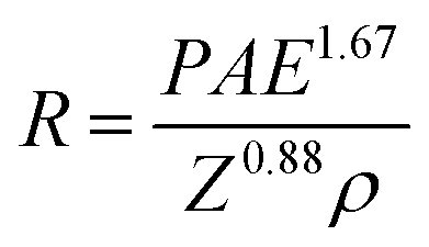
Fig. 3 exhibits numerical simulation and experiment results and provides more details about how to reduce irradiation damage to the material under ice. Distributions of absorbed energy in ice films with various primary beam energies are obtained by Monte Carlo electron trajectory simulation.29,30 It is worth noting that the whole interaction volume does not represent the actual volume in which electron-induced decomposition of H2O occurs. Nevertheless, in such a simulation we can roughly know how long the electron would travel in the ice, i.e., electron penetration depth, which provides a guide for determining the ice thickness in experiments to stop the electron reaching the underlying MoS2. As illustrated in Fig. 3a, at least 2 μm-thick ice is needed to prevent incident electrons of 10 keV from going through, while 50 nm is thick enough for the 1 keV. Fig. 3b shows quantitative relationship between electron penetration depth and primary beam energy. In addition to the Monte Carlo simulation, electron penetration depth can be calculated by the following empirical formula:31
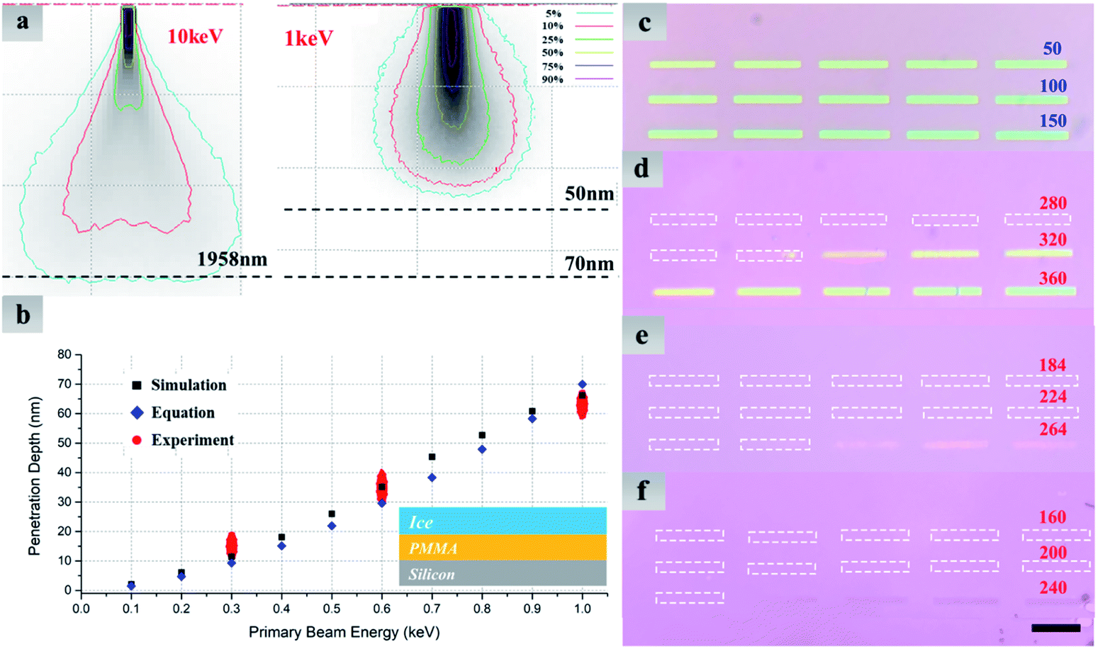 | ||
| Fig. 3 Simulation and experiment results on electron penetration depth. (a) Distributions of absorbed energy in ice films with primary beam energies of 1 keV and 10 keV. (b) Relationship between penetration depth and primary beam energy. Data are extracted from Monte Carlo simulations (black square), theoretical calculation (blue diamond) and experimental measurements (red oval). (c–f) Optical images of exposed PMMA to verify the protecting effect of an in situ formed ice layer. Electron dose for each rectangular area uniformly increases from left to right, top to bottom. (c) Direct exposure of 200 nm-thick PMMA by 1 keV e-beam. Exposure of PMMA with a 300 nm-thick ice layer on top by (d) 1 keV, (e) 0.6 keV and (f) 0.3 keV e-beam, respectively. White dotted lines indicate unaffected PMMA after exposure. Dose units are μC cm−2 in (c) and mC cm−2 in (d–f). Scale bar is 10 μm. | ||
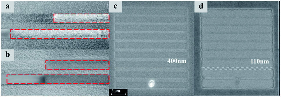
We have also designed experiments to find out the electron penetration depth at a specific energy. A 200 nm-thick polymethyl methacrylate (PMMA) film was spin-coated on a SiO2/Si substrate, on top of which water ice was vapor-deposited. The PMMA film thus acted as a ‘sensing layer’ to determine the critical dose when electrons could penetrate the ice. A 3 × 5 array of rectangles was directly exposed by evenly increasing electron dose from 10 μC cm−2 to 300 μC cm−2 at 1 keV (Fig. 3c). It is clearly seen that the minimum dose (10 μC cm−2) is enough to affect the PMMA. For contrast, Fig. 3d–f show optical images of exposed PMMA, which was covered by a 300 nm-thick ice layer before e-beam exposure. The minimum dose required to change the solubility of PMMA has been increased by 4 orders of magnitude, and these extra electrons are used for thinning the initial ice layer until low-energy electrons could penetrate it. The penetration depth is thus identified as the minimum ice thickness remaining for protecting the PMMA. For instance, the penetration depth at 1 keV approaches to the remained ice thickness using electron dose of 296 mC cm−2 (Fig. 3d). Benefitting from the linear feature of contrast curve of water ice,33 we could estimate such a remaining thickness using h = (1 − D/Ds)H. H represents the initial ice thickness, which can be measured by SEM imaging of tilted samples. D and Ds are electron dose used for exposure and the minimum dose for eliminating all ice, respectively.
The conformal sublimation of ice at 160 K has been recorded in Fig. 4. The temperature rise is controlled by adjusting the voltage of an electric resistance heater fixed under the sample stage. Fig. 4a and b show SEM images of the ice before and after sublimation. The initial ice thickness at 130 K is 400 nm, and the width of the exposed area (red dotted lines) is around 100 nm. After heating up, the remained ice within the exposed area is completely removed while the pattern shape is preserved. Fig. 4c and d display the broadening effect after heating the ice for more than one hour. The width of the gap surrounded by white dotted lines shrinks from 400 nm to 100 nm and other narrower ice gaps are sublimated.
 | ||
| Fig. 4 Controllable sublimation of remained ice. (a) SEM image of ice pattern at 130 K. Red dotted lines show exposed areas. (b) Pattern in (a) after heating at 160 K for 30 minutes. Remained ice within exposed areas has been eliminated. (c) Nanogaps fabricated on ice at 130 K. (d) Pattern in (c) after heating at 160 K for 60 minutes. | ||
In summary, we propose a modified lithographic method for patterning electron beam-sensitive materials. Water ice is condensed on top of monolayer MoS2 as a resist, which can be spatially divided into a top sacrificial layer and bottom protecting layer. E-beam patterning is only performed in the sacrificial layer. A series of exposure tests on ice/PMMA structures confirm that the e-beam induced radiolysis damage could be avoided by using low-energy electrons and a protecting ice layer thicker than the electron penetration depth. Subsequent sublimation process allows the protective ice to be removed, meanwhile, the shape of the pattern is kept. Back-gate FETs with ohmic contacts can be produced in this method, while poor contact is obtained without using a protecting layer. By altering the primary beam energy, electrical insulation or connection on MoS2 could be selectively achieved as needed, which is of great potential in fabricating optoelectronic devices based on 2D materials. Thanks to the solvent-free feature of iEBL, our method can also be applied to construct devices based on materials like perovskites or metal–organic frameworks, which are sensitive to both electron irradiation and organic solutions.
Author contributions
Conceptualization by G. Y. and D. Z.; data curation by G. Y.; funding acquisition by D. Z. and M. Q.; investigation by G. Y., Y. H. and R. Z.; methodology by D. Z. and G. Y.; writing-original draft by G. Y. and D. Z.; writing-review and editing by G. Y., D. Z. and M. Q.Conflicts of interest
There are no conflicts to declare.Acknowledgements
The authors gratefully acknowledge the support from the National Natural Science Foundation of China (61927820, 52076115).References
- W. T. Chen, A. Y. Zhu and F. Capasso, Nat. Rev. Mater., 2020, 5, 604–620 CrossRef.
- E. Ozbay, Science, 2006, 311, 189–193 CrossRef CAS PubMed.
- A. Dathbun, Y. Kim, Y. Choi, J. Sun, S. Kim, B. Kang, M. S. Kang, D. K. Hwang, S. Lee, C. Lee and J. H. Cho, ACS Appl. Mater. Interfaces, 2019, 11, 18571–18579 CrossRef CAS PubMed.
- Y. Ye, L. Gan, L. Dai, Y. Dai, X. Guo, H. Meng, B. Yu, Z. Shi, K. Shang and G. Qin, Nanoscale, 2011, 3, 1477–1481 RSC.
- X. Zheng, A. Calò, E. Albisetti, X. Liu, A. S. M. Alharbi, G. Arefe, X. Liu, M. Spieser, W. J. Yoo, T. Taniguchi, K. Watanabe, C. Aruta, A. Ciarrocchi, A. Kis, B. S. Lee, M. Lipson, J. Hone, D. Shahrjerdi and E. Riedo, Nat. Electron., 2019, 2, 17–25 CrossRef CAS.
- C. H. Lin, B. Cheng, T. Y. Li, J. R. D. Retamal, T. C. Wei, H. C. Fu, X. Fang and J. H. He, ACS Nano, 2019, 13, 1168–1176 CAS.
- R. Zan, Q. M. Ramasse, R. Jalil, T. Georgiou, U. Bangert and K. S. Novoselov, ACS Nano, 2013, 7, 10167–10174 CrossRef CAS PubMed.
- T. Lehnert, O. Lehtinen, G. Algara-Siller and U. Kaiser, Appl. Phys. Lett., 2017, 110, 033106 CrossRef.
- G. Imamura and K. Saiki, ACS Appl. Mater. Interfaces, 2015, 7, 2439–2443 CrossRef CAS PubMed.
- C. Xiao, Z. Li, H. Guthrey, J. Moseley, Y. Yang, S. Wozny, H. Moutinho, B. To, J. J. Berry, B. Gorman, Y. Yan, K. Zhu and M. Al-Jassim, J. Phys. Chem. C, 2015, 119, 26904–26911 CrossRef CAS.
- S. Ghosh, P. Kumar, S. Conrad, M. Tsapatsis and K. A. Mkhoyan, Microsc. Microanal., 2019, 25, 1704–1705 CrossRef.
- W. Song, L. Kong, Q. Tao, Q. Liu, X. Yang, J. Li, H. Duan, X. Duan, L. Liao and Y. Liu, Small, 2021, 17, e2101209 CrossRef PubMed.
- A. Han, A. Kuan, J. Golovchenko and D. Branton, Nano Lett., 2012, 12, 1018–1021 CrossRef CAS PubMed.
- A. Han, D. Vlassarev, J. Wang, J. A. Golovchenko and D. Branton, Nano Lett., 2010, 10, 5056–5059 CrossRef CAS PubMed.
- Y. Hong, D. Zhao, D. Liu, B. Ma, G. Yao, Q. Li, A. Han and M. Qiu, Nano Lett., 2018, 18, 5036–5041 CrossRef CAS PubMed.
- Y. Hong, D. Zhao, J. Wang, J. Lu, G. Yao, D. Liu, H. Luo, Q. Li and M. Qiu, Nano Lett., 2020, 20, 8841–8846 CrossRef CAS PubMed.
- R. F. Egerton, Microsc. Res. Tech., 2012, 75, 1550–1556 CrossRef CAS PubMed.
- A. E. Goode, A. E. Porter, M. M. Kłosowski, M. P. Ryan, S. Heutz and D. W. McComb, Curr. Opin. Solid State Mater. Sci., 2017, 21, 55–67 CrossRef CAS.
- Q. Chen, C. Dwyer, G. Sheng, C. Zhu, X. Li, C. Zheng and Y. Zhu, Adv. Mater., 2020, 32, e1907619 CrossRef PubMed.
- G. M. King, G. Schürmann, D. Branton and J. A. Golovchenko, Nano Lett., 2005, 5, 1157–1160 CrossRef CAS PubMed.
- Y. Hong, D. Zhao, D. L. Liu, G. G. Yao and M. Qiu, Microelectron. Eng., 2020, 224, 111251 CrossRef CAS.
- D. Zhao, A. Han and M. Qiu, Sci. Bull., 2019, 64, 865–871 CrossRef.
- G. Yao, D. Zhao, Y. Hong, S. Wu, D. Liu and M. Qiu, Nanoscale, 2020, 12, 22473–22477 RSC.
- K. D. Schock, F. E. Prins, S. Strähle and D. P. Kern, J. Vac. Sci. Technol., B: Microelectron. Nanometer Struct.--Process., Meas., Phenom., 1997, 15, 2323 CrossRef CAS.
- P. A. Peterson, Z. J. Radzimski, S. A. Schwalm and P. E. Russell, J. Vac. Sci. Technol., B: Microelectron. Nanometer Struct.--Process., Meas., Phenom., 1992, 10, 3088 CrossRef CAS.
- H. Yang, A. Jin, Q. Luo, C. Gu, Z. Cui and Y. Chen, Microelectron. Eng., 2006, 83, 788–791 CrossRef CAS.
- K. M. Satyalakshmi, A. Olkhovets, M. G. Metzler, C. K. Harnett, D. M. Tanenbaum and H. G. Craighead, J. Vac. Sci. Technol., B: Microelectron. Nanometer Struct.--Process., Meas., Phenom., 2000, 18, 3122 CrossRef CAS.
- L. K. Mun, D. Drouin, E. Lavallee and J. Beauvais, Microsc. Microanal., 2004, 10, 804–809 CrossRef CAS PubMed.
- D. Drouin, A. R. Couture, D. Joly, X. Tastet, V. Aimez and R. Gauvin, Scanning, 2007, 29, 92–101 CrossRef CAS PubMed.
- H. Demers, N. Poirier-Demers, A. R. Couture, D. Joly, M. Guilmain, N. de Jonge and D. Drouin, Scanning, 2011, 33, 135–146 CrossRef CAS PubMed.
- K. Kanaya and S. Okayama, J. Phys. D: Appl. Phys., 1972, 5, 43 CrossRef CAS.
- P. Jenniskens and D. F. Blake, Science, 1994, 265, 753–756 CrossRef CAS PubMed.
- S. Wu, D. Zhao, G. Yao, Y. Hong and M. Qiu, Appl. Surf. Sci., 2021, 539, 148265 CrossRef CAS.
| This journal is © The Royal Society of Chemistry 2022 |