
 Open Access Article
 This Open Access Article is licensed under a Creative Commons Attribution-Non Commercial 3.0 Unported Licence
Electrostatic control of photoluminescence from A and B excitons in monolayer molybdenum disulfide†
Yuchun
Liu
 ,
Tianci
Shen
,
Shuangyi
Linghu
,
Ruilin
Zhu
and
Fuxing
Gu
*
,
Tianci
Shen
,
Shuangyi
Linghu
,
Ruilin
Zhu
and
Fuxing
Gu
*
School of Optical-Electrical and Computer Engineering, University of Shanghai for Science and Technology, China. E-mail: gufuxing@usst.edu.cn
First published on 23rd April 2022
Abstract
Tailoring excitonic photoluminescence (PL) in molybdenum disulfide (MoS2) is critical for its various applications. Although significant efforts have been devoted to enhancing the PL intensity of monolayer MoS2, simultaneous tailoring of emission from both A excitons and B excitons remains largely unexplored. Here, we demonstrate that both A-excitonic and B-excitonic PL of chemical vapor deposition (CVD)-grown monolayer MoS2 can be tuned by electrostatic doping in air. Our results indicate that the B-excitonic PL changed in the opposite direction compared to A-excitonic PL when a gate voltage (Vg) was applied, both in S-rich and Mo-rich monolayer MoS2. Through the combination of gas adsorption and electrostatic doping, a 12-fold enhancement of the PL intensity for A excitons in Mo-rich monolayer MoS2 was achieved at Vg = −40 V, and a 26-fold enhancement for the ratio of B/A excitonic PL was observed at Vg = +40 V. Our results demonstrate not only the control of the conversion between A0 and A−, but also the modulation of intravalley and intervalley conversion between A excitons and B excitons. With electrostatic electron doping, the population of B excitons can be promoted due to the enhanced intravalley and intervalley transition process through electron–phonon coupling. The electrostatic control of excitonic PL has potential applications in exciton physics and valleytronics involving the B excitons.
Introduction
Two-dimensional (2D) transition metal dichalcogenides (TMDCs), especially molybdenum disulfide (MoS2), have drawn worldwide attention due to their unique optical and electronic properties.1–3 In particular, monolayer MoS2 presents strong photoluminescence (PL) and large exciton binding energy, providing a new platform to realize the emerging developments in various ultrathin optoelectronic devices.1,4–8 Due to the extremely large Coulomb interactions in atomically thin MoS2, stable excitons can be generated from the electron–hole pairs induced by photoexcitation even at room temperature. Generally, PL in monolayer MoS2 is dominated by the recombination of electrons in the conduction band with holes in the spin–orbit split valence bands, which refers to the A excitons and B excitons at the direct bandgap transition at the K and K′ points. The energy of B-excitonic PL peaks is 100–200 meV higher than that of A excitons, corresponding to the valence band splitting due to the strong spin orbital.9,10 Various intrinsic defects widely exist in MoS2, which act as active centers for trapping molecules and chemical reactions. These defects greatly impact the carrier concentration, exciton dynamics, and bandgap structure. Controlling the defects and carrier density is an effective method for modulating the PL properties of monolayer MoS2.11,12 Enhanced PL emission is generally achieved by promoting defect-related doping and trion-exciton transitions. The most widely reported strategies include depleting excessive electrons through gas physisorption,13–15 chemical doping16,17, and direct carrier injection through electrical doping.18,19 The O2, H2O and N2 molecules can be directly adsorbed on chalcogen vacancies and electrons extracted from MoS2.13,14 The previous work involving chemical doping with bis(trifluoromethane) sulfonimide (TFSI), poly(4-styrenesulfonate) (PSS) and 7,7,8,8-tetracyanoquinodimethane (TCNQ) drastically enhanced the PL intensity of monolayer MoS2. The electrically doped MoS2 monolayers encapsulated in poly(methyl methacrylate) achieved a marked PL enhancement and near-unity quantum yields due to the mechanism of electron counter-doping without chemical defect passivation.1 Indeed, extensive studies on the PL properties and exciton dynamics in MoS2 have been reported, which focus on the interplay between neutral A excitons (A0) and many-body bound states such as charged trions (A−).20–22 However, these studies are limited to the enhancement of A-excitonic PL emission and valley polarization.The B-exciton emission of monolayer MoS2 has only been investigated in a few studies.23–26 It has been reported that PL emissions from both A and B excitons can vary widely from sample to sample, which is related to the difference in non-radiative recombination associated with defect density in a given sample. B excitons exhibit a monotonic decline as the defect density increases in the monolayer MoS2 prepared by the chemical vapor deposition (CVD) method.24 Mikkelsen et al. demonstrated tunable emission wavelengths of the A and B excitons in monolayer MoS2 by tuning the plasmonic nanocavity resonance; this method successfully achieved a dominant B-excitonic emission by overlapping the plasmon resonance with the B exciton energy.25,26 McCreary et al. provided a facile method to assess sample quality: a low B/A ratio indicates a low defect density and high sample quality, while a large B/A ratio represents a high defect density and poor-quality material.27 Sarkar et al. obtained a six-fold enhancement of the intrinsically weak B excitonic emission in few layers of MoS2![[thin space (1/6-em)]](https://www.rsc.org/images/entities/char_2009.gif) :Ag nano-heterojunctions embedded into a glass matrix, which can be attributed to the dipole–dipole interactions via exciton–plasmon coupling at room temperature.28 The simultaneous tailoring of emission form both A excitons and B excitons remains largely unexplored.
:Ag nano-heterojunctions embedded into a glass matrix, which can be attributed to the dipole–dipole interactions via exciton–plasmon coupling at room temperature.28 The simultaneous tailoring of emission form both A excitons and B excitons remains largely unexplored.
In this study, we explored the tunable excitonic PL from both A excitons and B excitons in monolayer MoS2 on SiO2/Si substrates prepared by the traditional CVD method. Electrostatic doping was performed through back-gate voltage (Vg) variation in a capacitor structure, demonstrating an effective control method for both A-excitonic and B-excitonic PL in monolayer MoS2 in air at room temperature. Electrostatic doping allowed us to tune the B-excitonic PL intensity in a direction opposite to the A-excitonic PL. Electron injection induced by a positive Vg obviously enhanced the PL intensity from B excitons, while the A-excitonic PL was suppressed in both S-rich and Mo-rich monolayer MoS2. Our results not only demonstrate good control of conversion between A0 and A− through a combination of gas adsorption and electrostatic doping, but also show the presence of intravalley and intervalley transitions between A excitons and B excitons. The B excitons would relax to A excitons when a negative Vg was applied, leading to reduced B-excitonic PL and increased A-excitonic PL. When the applied Vg became positive, the B exciton population was increased due to the enhanced intravalley and intervalley transitions from A excitons. These transitions can be mediated by flexural phonons in the realm of the Elliott–Yafet spin-flip mechanism through intrinsic electron–phonon scattering. Experimental results show that excitonic PL from both A and B excitons was effectively controlled by the electrostatic method. This could pave an additional pathway for investigating exciton physics and valleytronics in 2D TMDCs at room temperature.
Experimental section
Monolayer MoS2 was prepared on SiO2/Si substrates (280–300 nm SiO2) by the CVD method in a double-zone furnace. Sulfur powder and molybdenum(VI) oxide (MoO3) powder were used as precursors, with sulfur placed upstream and MoO3 placed downstream of the two-zone furnace, respectively (as shown in Fig. S1 of the ESI†). The temperature of the central zone-I and zone-II were set to 300 °C and 850–870 °C for the sulfur and molybdenum precursor, respectively. High-purity argon gas (Ar) was introduced into a quartz tube with a flow rate of 100–150 sccm during the growth process. The growth time was about 10–20 minutes for monolayer MoS2 in our growth system at nearly atmospheric pressure. The monolayer MoS2 flakes with different qualities can be achieved by changing the Mo:S ratio of the precursor and the gas flow rate.29–32 For the growth of S-rich monolayer MoS2, 200 mg sulfur powder and 5 mg MoO3 powder were used as precursors with an Ar flow rate of 100–120 sccm. For the growth of Mo-rich monolayer MoS2, 200 mg sulfur powder and 10 mg MoO3 powder were used as precursors with an Ar flow rate of 150 sccm.
Optical microscopy, atomic force microscopy (AFM), and Raman spectroscopy were used to characterize the CVD-grown monolayer MoS2. Then a Au electrode was fabricated by sputtering with polydimethylsiloxanes (PDMS) masks at the micron scale. Electrostatic doping was conducted based on MoS2 samples in a structure similar to a field-effect transistor (FET), with Au as the top electrode and Si as the back-gate electrode. PL spectra were collected using an IsoPlane spectrometer equipped with an emICCD (Princeton Instruments, PI-MAX4) under 532 nm continuous wave (CW) laser excitation. The Raman measurements were taken by using a Renishaw inVia Raman microscope under 532 nm laser excitation. The laser power intensity was ∼103 W cm−2 for PL and Raman spectra measurements with a spot size of ∼2 μm. The electrostatic doping in the MoS2 monolayer was systematically varied by using a DC voltage supplier. The MoS2 samples exhibited electrostatic doping over the range of the gate voltage (−40 V to +40 V). All measurements were performed at room temperature under ambient air conditions.
Results and discussion
Fig. 1(a) shows the microscopy image of monolayer MoS2 prepared by the CVD method. The thickness of triangular CVD-grown MoS2 was ∼0.85 nm, which is consistent with the monolayer thickness. The size of triangular monolayer MoS2 was 30–70 μm. The absorption spectra and Raman spectra of the MoS2 grown on SiO2/Si substrates under relatively S-rich and Mo-rich conditions are shown in Fig. 1(b–c). Two distinguishing absorption peaks were observed in both S-rich and Mo-rich monolayer MoS2, which relate to the A and B excitons. The Raman spectra peaks were located at ∼384 cm−1 and ∼404.5 cm−1 corresponding to the E12g and A1g peaks for the in-plane and out-of-plane vibration modes, respectively. The frequency differences (Δ) between E12g and A1g peaks were 20.6 cm−1 and 20.3 cm−1 for the S-rich and Mo-rich MoS2, respectively, in accordance with the observed separation in the CVD-grown monolayer MoS2 on SiO2/Si.33 It has been reported that n-type doping leads to a redshift of the A1g peak and an increased line width of A1g, whereas the E12g peak is insensitive to the doping effect.34,35 The Mo-rich MoS2 sample showed a red-shifted A1g peak at 404.2 cm−1, compared to that of the S-rich MoS2 sample at 404.7 cm−1. The Raman mode peaks of MoS2 grown on SiO2/Si substrates were plotted on the Raman-derived doping-strain map, as shown in Fig. 1(d). The zero strain and zero doping lines crossed at a point, corresponding to the literature values (E12g = 385.0.2 cm−1 and A1g = 405.0 cm−1) of the peak frequencies for a suspended MoS2 membrane.36–38 The correlation plot of the A1g peak positions versus the E12g peak positions suggest that the Mo-rich MoS2 grown on SiO2 shows a higher electron doping (2–3 × 1012 cm−2) than that of the S-rich MoS2 (0.5–1 × 1012 cm−2). Raman peaks of both Mo-rich and S-rich MoS2 were located near a strain line at ε = 0.2%, indicting no obvious difference in the strain effect. Therefore, the peak shifts between the Mo-rich and S-rich MoS2 in the absorption spectra could be attributed to the different electron doping effects. The AFM morphology and surface potential mapping for the monolayer Mo-rich and S-rich MoS2 with a Au electrode on SiO2/Si substrates are shown in Fig. S2.† The CVD-grown Mo-rich MoS2 exhibited a work function of ∼96 meV, which is lower than that of the S-rich MoS2.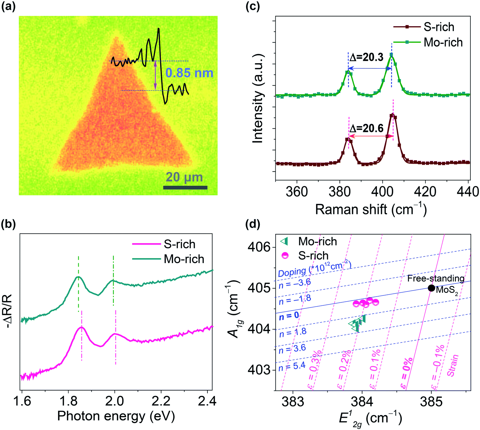 | ||
| Fig. 1 (a) Microscopy image of the CVD-grown MoS2 on a SiO2/Si substrate; (b–d) Absorption spectra, Raman spectra, and the correlation plot (A1gversus E12g) of the S-rich and Mo-rich monolayer MoS2. | ||
A configuration similar to a back-gated FET was used for electrostatically controlled excitonic PL emission in CVD-grown monolayer MoS2 on a SiO2/Si substrate, as shown in Fig. 2(a). The PL spectra of our MoS2 samples without electrostatic doping in Fig. 2(b) exhibit clear peaks at 1.83–1.86 eV (A-excitonic emission) and an inconspicuous peak at near 2.0 eV (B-excitonic emission). This MoS2 monolayer on a SiO2/Si substrate showed PL bands that were red-shifted with respect to the peak positions of high-quality exfoliated monolayers, which is typical of the CVD-grown monolayer MoS2 and caused by intrinsic strain and defects. The S-rich MoS2 sample also presented a blue-shifted PL peak with a PL intensity that was 2.2-fold higher compared to the Mo-rich MoS2 under laser excitation with a power intensity of <103 W cm−2. The greater PL emission observed in the S-rich MoS2 is consistent with the Raman spectra results. Fig. 2(c and d) presents the PL spectra at different Vg for the S-rich and Mo-rich MoS2 samples with Au and P+–Si as the electrodes. Both the S-rich and Mo-rich MoS2 samples exhibited remarkably gate-dependent excitonic PL emission. Application of a negative Vg enhanced the A-excitonic PL intensity, while an applied positive Vg markedly reduced the A-excitonic PL. The PL peak positions of the S-rich MoS2 remained almost constant at ∼1.855 eV for the main excitonic PL within a range of −40 V to +40 V of the applied Vg. However, in the Mo-rich MoS2 samples, both the PL intensity and PL peak positions were noticeably changed. The main excitonic PL peak of the Mo-rich MoS2 was located at 1.835 eV at Vg = 0 V, and then shifted to 1.823 eV at Vg = +40 V and 1.851 eV at Vg = −40 V, respectively.
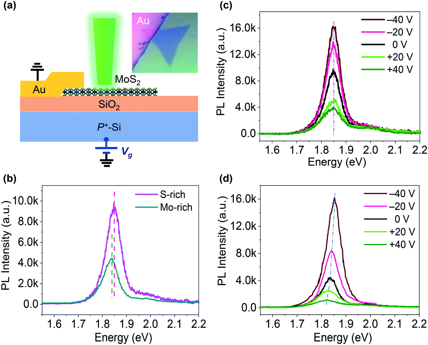 | ||
| Fig. 2 (a) Schematic diagram of the experimental setup for the electrostatic doping of CVD-grown MoS2; inset: optical image of the sample; (b) PL spectra of the monolayer MoS2 samples without electrostatic doping; (c and d) PL spectra at various Vg for (c) S-rich MoS2 and (d) Mo-rich MoS2. | ||
To clarify the changes in A-excitonic and B-excitonic PL emission at different applied Vg, the PL spectra of MoS2 were fitted with Lorentzian curves. The three peaks were denoted by the emission of neutral excitons (A0), trions (A−) and B excitons. The gate-dependent PL spectral fittings of the S-rich MoS2 sample are shown in Fig. 3, with three PL peaks at 1.86 eV, 1.82 eV and 2.00 eV. A negative Vg could enhance the A-excitonic PL intensity (A0 and A−), but decrease the PL intensity from B excitons. When the Vg was adjusted to the positive range, the A-excitonic PL decreased, but B-excitonic PL increased and the peak became obvious. Quantitative analysis was conducted to assign the changes in PL intensity to the contribution of A0, A− or B. The normalized PL at various Vg suggested almost unshifted PL peaks and obvious changes in the B-excitonic PL intensity. The respective PL intensity and relative spectral weight distribution can be attributed to the free electron density in monolayer MoS2, which can be changed by the applied Vg and gaseous environments. Fig. 3(f) shows the PL intensity ratio of A0 and A− (Iexciton/Itrion) of the S-rich MoS2 at different Vg. The Iexciton/Itrion ratio decreased monotonically from 2.08 to 0.86 as the Vg was adjusted from −40 V toward +40 V.
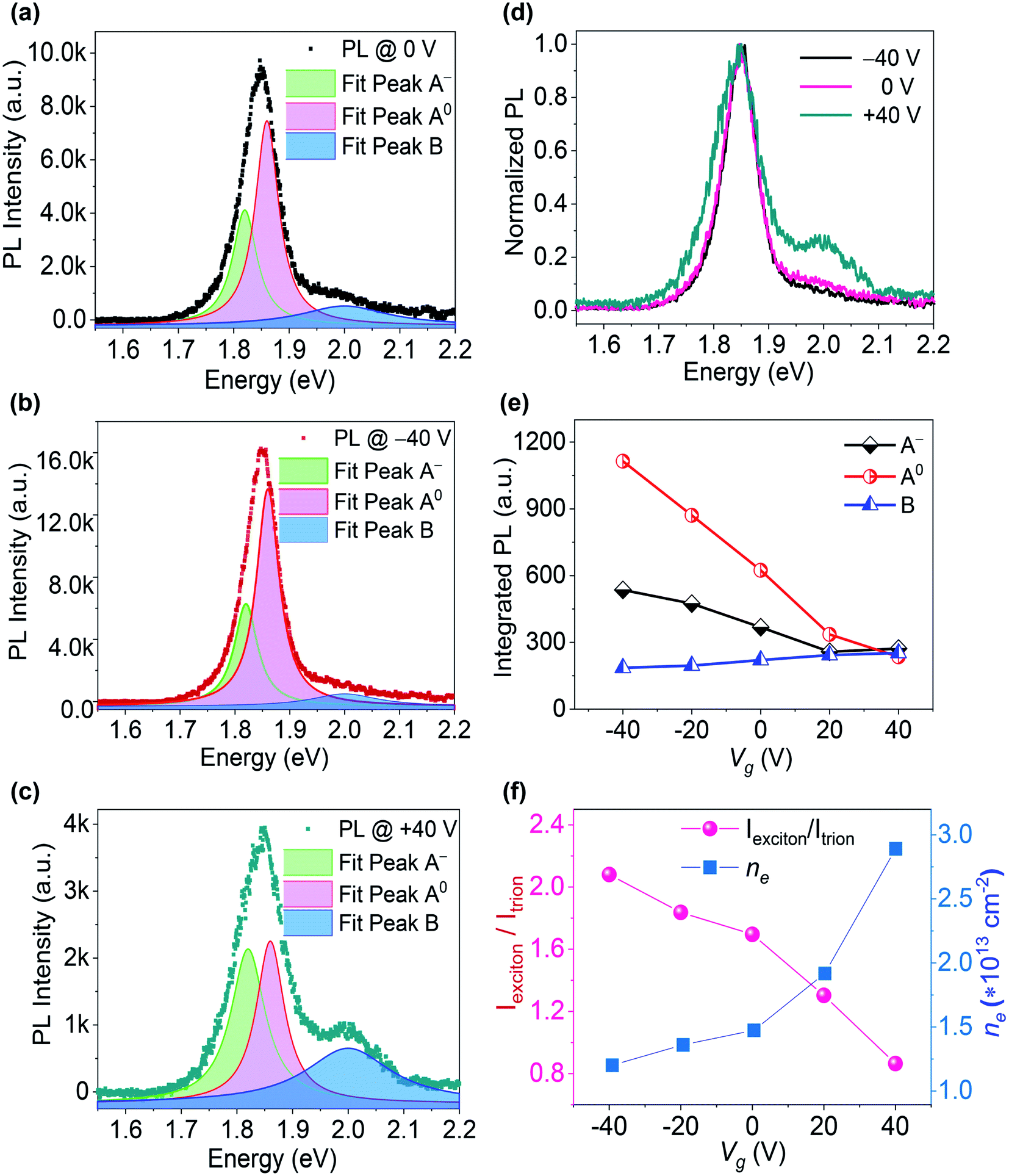 | ||
| Fig. 3 Gate-dependent PL properties of the S-rich monolayer MoS2 sample: (a–c) PL at Vg = 0 V, −40 V and +40 V, fitted by using the Lorentzian function; (d) normalized PL at Vg = 0 V, −40 V, and +40 V; (e) integrated PL intensities of A0, A−, and B; (f) ratio of the integrated PL intensities of A0 and A−versus Vg, and calculated electron density versus Vg. | ||
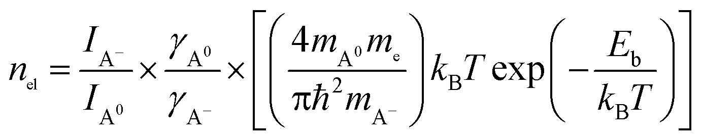
The electron density nel in monolayer MoS2 can be estimated from the PL intensity analysis of neutral exciton and trion emissions according to the mass action model based on the dynamic equilibrium between A excitons (A0 and A−) and free electrons, which can be expressed as:15,39
 | (1) |
The gate-dependent PL spectra of the Mo-rich MoS2 sample were fitted with the Lorentzian function, with three peaks denoted by the emissions of A0, A−, and B excitons, corresponding to the energies of 1.852 eV, 1.812 eV and 1.962 eV, respectively. As shown in Fig. 4, the A-excitonic PL intensity decreased when Vg changed from −40 V to +40 V, but the B-excitonic PL increased and the peak became obvious. The quantitative analysis can assign the changes in PL intensity to the contributions of A0, A−, and B. The normalized PL at various Vg suggested the shifted A-excitonic PL peaks and obvious changes in B-excitonic PL intensity. The PL emission of A0 and A− steadily decreased and the B-excitonic PL intensity increased monotonically when Vg was adjusted from −40 V to +40 V. As shown in Fig. 4(f), the Iexciton/Itrion ratio of Mo-rich MoS2 decreased monotonically from 1.69 to 0.18 as Vg was changed from −40 V toward +40 V. The calculated value of the electron density nel in Mo-rich MoS2 was ∼3.36 × 1013 cm−2 at Vg = 0 V, ∼1.48 × 1013 cm−2 at Vg = −40 V, and ∼1.42 × 1014 cm−2 at Vg = +40 V. Moreover, the statistical value of the PL intensity ratio for both the S-rich and Mo-rich MoS2 with error bars were obtained from more than 10 tests, as shown in Fig. S3.† At Vg = −40 V, the A-excitonic PL intensity ratio Iexciton/Itrion of Mo-rich MoS2 was approximately 12-fold that of the ratio at Vg = +40 V. The PL intensity ratio of B and A excitons (IB/IA) was approximately 26 times higher at Vg = +40 V, compared to that at Vg = −40 V. Both the Iexciton/Itrion and IB/IA ratios in Mo-rich MoS2 were more sensitive to the applied Vg than that in S-rich MoS2.
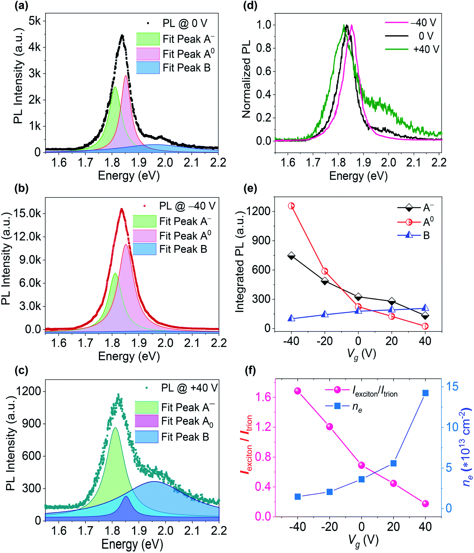 | ||
| Fig. 4 Gate-dependent PL properties of the Mo-rich monolayer MoS2 sample: (a–c) PL at Vg = 0 V, −40 V and +40 V, fitted with the Lorentzian function; (d) normalized PL at Vg = 0 V, −40 V and +40 V; (e) integrated PL intensities of A0, A−, and B; (f) ratio of the integrated PL intensities of A0 and A−versus Vg, and calculated electron density versus Vg. | ||
Generally, the as-prepared MoS2 is n-doped due to the presence of unavoidable defects or unintentional doping of substrates. The excitonic PL in monolayer MoS2 varies according to the changes in electron density and strain effects. By applying a negative Vg, holes are injected into MoS2 and bind with excess electrons to form A0 excitons, resulting in pronounced trion-exciton conversion and enhanced PL intensity in the A-exciton band. The enhanced A0 and A− emission can be attributed to the suppression of non-radiative recombination of A0 and A− at the defect sites, as well as the proposed transition from B to A exciton recombination. Meanwhile, at a positive Vg, n-type doping with injected electrons facilitates the increased formation of A−, leading to a decrease in both the A0 exciton density and total PL intensity. The probability of forming excitons and trions is expected to rapidly decrease at a high electron density in MoS2 due to the nonradiative recombination via the Auger process, which leads to a low PL intensity from A excitons. The excitonic PL intensity from A− decreased monotonically even when the applied Vg changed from negative to positive in our experiment. The trion PL in our study seems more sensitive to Vg than that in the former reported results, where the trion PL is nearly gate independent or exhibits weak gate bias dependence.
The applied gate voltage can be converted to the charge carrier doping density (Δninjected = CVg/e), where C = ε0εr/d, ε0 = 8.85 × 10⁻¹² F m−1, εr = 3.9, and d = 280 nm. The injected hole density was ∼3 × 1012 cm−2 at Vg = −40 V, while the injected electron density was ∼3 × 1012 cm−2 at Vg = +40 V. It should be noted that in the S-rich MoS2 sample, the calculated Δninjected was almost equivalent to the inferred electron density change (Δnel) from Iexciton/Itrion at Vg = −40 V but much smaller than that at Vg = +40 V. In the Mo-rich MoS2 sample, the calculated Δninjected was much smaller than the inferred Δnel at a both negative and positive Vg. Furthermore, the inferred Δnel from Iexciton/Itrion at Vg = −40 V was smaller than that at Vg = +40 V in both the S-rich and Mo-rich MoS2 samples. The different electron density changes Δnel in S-rich and Mo-rich MoS2 could be attributed to the different gas adsorption situations of MoS2 at a positive and negative Vg.
Sulfur vacancies in monolayer MoS2 have the lowest formation energy and can act as active centers for trapping molecules and chemical reactions. Generally, the physically and chemically adsorbed ambient gas molecules on the MoS2 surface can reduce the electron density and enhance the PL intensity with a blue shift.40–42 Due to the interactions of O2 and H2O molecules with S vacancies, charge transfer from defective MoS2 to O2/H2O leads to a decrease in the relative trion intensity.43 Considering the basic electrostatics theory, the SiO2–MoS2 interface either attracts electrons or repels electrons to or from O2, depending on the polarity.44 Charge transfer between the adsorbed molecule and MoS2 can even be significantly modulated by a perpendicular electric field.45 Therefore, the physically adsorbed molecules on monolayer MoS2 can act as either charge acceptors or donors, depending on the situation. The applied Vg can consistently modify the charge transfer between the adsorbed molecules and monolayer MoS2. Since the electron density is further reduced in MoS2 when a negative Vg was applied with hole-doping, the charge transfer from MoS2 to the adsorbed molecules could be suppressed. Meanwhile, the positive Vg induced by electron-doping resulted in an increased density of electrons in MoS2, which may affect the charge transfer between MoS2 and O2/H2O molecules, and lead to an adsorption situation different from that of MoS2 at a negative Vg. Since the position of the Fermi level can significantly influence the adsorption and desorption processes of oxygen molecules on the surface,13,40 we suppose that the external absorption of O2/H2O molecules from the ambient environment partly depends on the different electrostatic dopings in monolayer MoS2. The S-rich MoS2 sample doped with PEDOT:PSS was used to confirm the effects of gas adsorption and surface defects. After doping with PEDOT:PSS, the sulfur vacancies can be healed spontaneously by the sulfur ad atom clusters through PSS-induced hydrogenation.17 The PEDOT:PSS layer even insulated MoS2 from the H2O/O2 in air, leading to suppressed charge transfer between the MoS2 surface and the gas molecules. Fig. S4† shows the PL spectra and integrated PL intensity of the doped MoS2 sample at different Vg. The PL intensity from A− in the doped MoS2 showed a weak dependence on Vg, similar to the results in previously reported studies. Thereby, the monotonic change in the intensity of A-excitonic PL as the Vg increased from −40 V to +40 V can be attributed to variations in charge density, which were simultaneously affected by electrostatic doping and gas adsorption in both S-rich and Mo-rich MoS2.
Another key issue is the PL emission of B excitons, which changes with electrostatic doping in MoS2. Generally, A and B excitons are quickly formed at K and K′ valleys under photo-excitation with circular polarization. After the excitons are generated, besides the direct excitonic radiative recombination at the K and K′ valleys, A and B excitons can also undergo intravalley and intervalley scattering before recombination, as shown in Fig. 5. The B excitons can serve as a population supplier to the energetically lower A excitons.46 As shown in Fig. 5(c) and (e), the rapid relaxation from B to A excitons reduces the available B-excitonic PL emission while simultaneously increasing the A-excitonic PL. Meanwhile, as shown in Fig. 5(d) and (f), the photoexcited electron with a spin-down state for the A exciton at the K valley can exhibit an intravalley spin reversal to occupy the electron spin-up state for the B exciton at the K valley, or exhibit intervalley scatter to the electron spin-down state for the B exciton at the K′ valley. The intravalley transition with electron spin reversal can be mediated by flexural phonons via the Elliott–Yafet spin-flip mechanism due to intrinsic electron–phonon scattering.47–49 These intravalley and intervalley transitions from A to B excitons can also be understood as a phonon-assisted process. Auger recombination leads to the annihilation of electrons in the conduction band and holes in valence sub-band A, while creating phonons coupled with electrons. Then, electron–phonon coupling contributes to the new formation of B excitons.
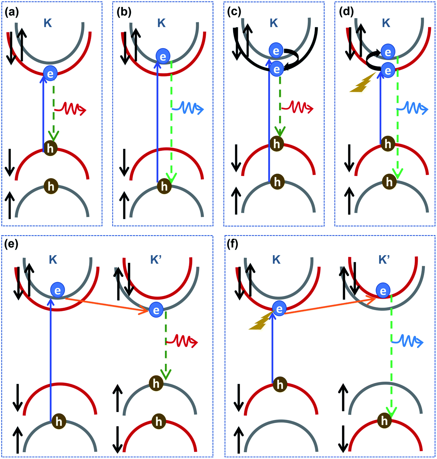 | ||
| Fig. 5 (a and b) Traditional excitonic radiative recombination at the K valley for A and B excitons, respectively; (c–f) intravalley and intervalley transition processes in monolayer MoS2: (c) at the K valley, a spin-up electron in the valence band (VB) is excited to the spin-up conduction band (CB), then it scatters to the spin-down CB at the K valley before A-excitonic recombination occurs; (d) at the K valley, a spin-down VB electron is excited to the spin-down CB, then phonon-assisted spin–flip intravalley scattering occurs before B-excitonic recombination; (e) at the K valley, a spin-up VB electron is excited to the spin-up CB, then intervalley scattering occurs before A-excitonic recombination at the K′ valley; (f) at the K valley, a spin-down VB electron is excited to the spin-down CB, then phonon-assisted intervalley scattering occurs before B-excitonic recombination at the K′ valley. | ||
Since the effective exciton lifetime of both A and B excitons are sensitive to the density of defects due to the induced non-radiative recombination pathways, the transition between A and B excitons would be affected by the defect density in MoS2. High electron density in MoS2 can result in significantly different non-radiative recombinations, resulting in a greater B exciton population available due to the phonon-assisted process. Furthermore, typical electrostatic gating and the dielectric environment of 2D materials can break the σh symmetry and induce electron–phonon coupling to the flexural phonon modes, which manifest in a linear dependence on the electron density via the gate voltages.50 Consequently, the increased electron–phonon coupling would enhance electron spin reversal when more electrons are injected into MoS2, leading to an obvious enhancement in the B exciton population with the phonon-assisted process. Thereby, we explain the observed increase of B excitonic emission with increasing electron density by considering the enhanced intravalley A-to-B exciton transition as a result of the phonon-assisted process. The B-excitonic PL intensity increased due to the transition from A to B excitons when more electrons were injected by a negative Vg, while the reduction of B-excitonic PL emission could be attributed to the B to A exciton relaxation effect in a hole-doping situation under the condition of a negative Vg.
Conclusions
In summary, excitonic PL from both A excitons and B excitons in monolayer CVD-grown MoS2 was investigated at room temperature. Electrostatic doping through Vg variation was shown to be an effective control method for the A-excitonic and B-excitonic PL in monolayer MoS2 with different defect densities. Electrostatic doping led to a change in the B-excitonic PL intensity that occurred in the opposite direction to changes in A-excitonic PL. The applied positive Vg promoted electron injection and obviously enhanced the PL intensity from B excitons, while the A-excitonic PL was suppressed in both S-rich and Mo-rich monolayer MoS2. Our results demonstrate not only the ability to control the conversion between A0 and A− through the combination of gas adsorption and electrostatic doping, but also the presence of transitions between A excitons and B excitons. The B excitons would relax to A excitons when a negative Vg was applied, leading to reduced B exciton population and increased A-excitonic PL. When the applied Vg became positive with electron doping, the population of B excitons was promoted due to the intravalley and intervalley transition from A excitons, which can be mediated by flexural phonons in the realm of the Elliott–Yafet spin–flip mechanism through electron–phonon coupling. In Mo-rich monolayer MoS2, a 12-fold increase in the A-excitonic PL intensity ratio Iexciton/Itrion was observed at a Vg of −40 V and an approximately 26-fold increase in IB/IA occurred at the applied Vg of +40 V. This electrostatic doping method could offer an important method for excitonic PL modulation. The efficient tunability of B-excitonic PL emission may provide potential applications in exciton physics and valleytronic devices involving the B excitons.Conflicts of interest
There are no conflicts to declare.Acknowledgements
This work was supported by the National Natural Science Foundation of China (NSFC, 62075131) and the China Postdoctoral Science Foundation (2020M671168).Notes and references
- M. Amani, D.-H. Lien, D. Kiriya, J. X. A. Azcatl, J. Noh, S. R. Madhvapathy, R. Addou, K. C. Santosh, M. Dubey, K. Cho, R. M. Wallace, S.-C. Lee, J.-H. He, J. W. Ager III, X. Zhang, E. Yablonovitch and A. Javey, Science, 2015, 350, 1065–1068 CrossRef CAS PubMed.
- F. Liao, J. Yu, Z. Gu, Z. Yang, T. Hasan, S. Linghu, J. Peng, W. Fang, S. Zhuang, M. Gu and F. Gu, Sci. Adv., 2019, 5, eaax7398 CrossRef CAS PubMed.
- N. Li, Q. Wang, C. Shen, Z. Wei, H. Yu, J. Zhao, X. Lu, G. Wang, C. He, L. Xie, J. Zhu, L. Du, R. Yang, D. Shi and G. Zhang, Nat. Electron., 2020, 3, 711–717 CrossRef CAS.
- D. Mouloua, A. Kotbi, G. Deokar, K. Kaja, M. E. Marssi, M. A. E. Khakani and M. Jouiad, Materials, 2021, 14, 3283 CrossRef CAS PubMed.
- Y. C. Liu and F. X. Gu, Nanoscale Adv., 2021, 3, 2117–2138 RSC.
- H. Wang, C. Li, P. Fang, Z. Zhang and J. Z. Zhang, Chem. Soc. Rev., 2018, 47, 6101–6127 RSC.
- D. B. Sulas-Kern, E. M. Miller and J. L. Blackburn, Energy Environ. Sci., 2020, 13, 2684–2740 RSC.
- T. Mueller and E. Malic, npj 2D Mater. Appl., 2018, 2, 29 CrossRef.
- X. Dou, K. Ding, D. Jiang, X. Fan and B. Sun, ACS Nano, 2016, 10, 1619–1624 CrossRef CAS PubMed.
- K. M. McCrearya, A. T. Hanbicki, V. S. Sa and B. T. Jonker, APL Mater., 2018, 6, 111106 CrossRef.
- Y. Cai, H. Zhou, G. Zhang and Y.-W. Zhang, Chem. Mater., 2016, 28, 8611–8621 CrossRef CAS.
- D.-H. Lien, S. Z. Uddin, M. Yeh, M. Amani, H. Kim, J. W. Ager, E. Yablonovitch and A. Javey, Science, 2019, 364, 468–471 CrossRef CAS.
- P. Klement, C. Steinke, S. Chatterjee, T. O. Wehling and M. Eickhoff, 2D Mater., 2018, 5, 045025 CrossRef CAS.
- P. K. Gogoi, Zh. Hu, Q. Wang, A. Carvalho, D. Schmidt, X. Yin, Y.-H. Chang, L.-J. Li, C. H. Sow, A. H. Castro Neto, M. B. H. Breese, A. Rusydi and A. T. S. Wee, Phys. Rev. Lett., 2017, 119, 077402 CrossRef PubMed.
- S. Mouri, Y. Miyauchi and K. Matsuda, Nano Lett., 2013, 13, 5944–5948 CrossRef CAS.
- M. Amani, R. A. Burke, X. Ji, P. Zhao, D.-H. Lien, P. Taheri, G. H. Ahn, D. Kirya, J. W. Ager III, E. Yablonovitch, J. Kong, M. Dubey and A. Javey, ACS Nano, 2016, 10, 6535–6541 CrossRef CAS.
- X. Zhang, Q. Liao, S. Liu, Z. Kang, Z. Zhang, J. Du, F. Li, S. Zhang, J. Xiao, B. Liu, Y. Ou, X. Liu, L. Gu and Y. Zhang, Nat. Commun., 2017, 8, 15881 CrossRef CAS.
- J. S. Ross, S. Wu, H. Yu, N. J. Ghimire, A. M. Jones, G. Aivazian, J. Yan, D. G. Mandrus, D. Xiao, W. Yao and X. Xu, Nat. Commun., 2013, 4, 1474 CrossRef PubMed.
- L. A. Jauregui, A. Y. Joe, K. Pistunova, D. S. Wild, A. A. High, Y. Zhou, G. Scuri, K. De Greve, A. Sushko, C.-H. Yu, T. Taniguchi, K. Watanabe, D. J. Needleman, M. D. Lukin, H. Park and P. Kim, Science, 2019, 366, 870–875 CrossRef CAS.
- J. Xiao, M. Zhao, Y. Wang and X. Zhang, Nanophotonics, 2017, 6(6), 1309–1328 CAS.
- K. F. Mak, K. He, C. Lee, G. H. Lee, J. Hone, T. F. Heinz and J. Shan, Nat. Mater., 2013, 12, 207–211 CrossRef CAS.
- M. Zhou, W. Wang, J. Lu and Z. Ni, Nano Res., 2021, 14, 29–39 CrossRef CAS.
- A. Steinhoff, J.-H. Kim, F. Jahnke, M. Rösner, D.-S. Kim, C. Lee, G. H. Han, M. S. Jeong, T. O. Wehling and C. Gies, Nano Lett., 2015, 15, 6841–6847 CrossRef CAS.
- K. Wu, Z. Li, J. Tang, X. Lv, H. Wang, R. Luo, P. Liu, L. Qian, S. Zhang and S. Yuan, Nano Res., 2018, 11, 4123–4132 CrossRef CAS.
- G. M. Akselrod, T. Ming, C. Argyropoulos, T. B. Hoang, Y. Lin, X. Ling, D. R. Smith, J. Kong and M. H. Mikkelsen, Nano Lett., 2015, 15, 3578–3584 CrossRef CAS.
- J. Huang, G. M. Akselrod, T. Ming, J. Kong and M. H. Mikkelsen, ACS Photonics, 2018, 5, 552–558 CrossRef CAS.
- K. M. McCrearya, A. T. Hanbicki, S. V. Sivaramb and B. T. Jonker, APL Mater., 2018, 6, 111106 CrossRef.
- A. S. Sarkar, I. Konidakis, I. Demeridou, E. Serpetzoglou, G. Kioseoglou and E. Stratakis, Sci. Rep., 2020, 10, 15697 CrossRef CAS.
- S. Wang, Y. Rong, Y. Fan, M. Pacios, H. Bhaskaran, K. He and J. H. Warner, Chem. Mater., 2014, 26, 6371–6379 CrossRef CAS.
- H. Liu, Y. Zhu, Q. Meng, X. Lu, S. Kong, Z. Huang, P. Jiang and X. Bao, Nano Res., 2017, 10, 643–651 CrossRef CAS.
- I. S. Kim, V. K. Sangwan, D. Jariwala, J. D. Wood, S. Park, K.-S. Chen, F. Shi, F. Ruiz-Zepeda, A. Ponce, M. Jose-Yacaman, V. P. Dravid, T. J. Marks, M. C. Hersam and L. J. Lauhon, ACS Nano, 2014, 8, 10551–10558 CrossRef CAS PubMed.
- D. Zhou, H. Shu, C. Hu, L. Jiang, P. Liang and X. Chen, Cryst. Growth Des., 2018, 18, 1012–1019 CrossRef CAS.
- Y. Zhan, Z. Liu, S. Najmaei, P. M. Ajayan and J. Lou, Small, 2012, 8, 966–971 CrossRef CAS PubMed.
- A. Tarasov, S. Zhang, M. Y. Tsai, P. M. Campbell, S. Graham, S. Barlow, S. R. Marder and E. M. Vogel, Adv. Mater., 2015, 27, 1175–1181 CrossRef CAS PubMed.
- M. W. Iqbal, K. Shahzad, R. Akbar and G. Hussain, Microelectron. Eng., 2020, 219, 111152 CrossRef CAS.
- W. H. Chae, J. D. Cain, E. D. Hanson, A. A. Murthy and V. P. Dravid, Appl. Phys. Lett., 2017, 111, 143106 CrossRef.
- S. E. Panasci, E. Schilirò, G. Greco, M. Cannas, F. M Gelardi, S. Agnello, F. Roccaforte and F. Giannazzo, ACS Appl. Mater. Interfaces, 2021, 13, 31248–31259 CrossRef CAS.
- G. Ciampalini, F. Fabbri, G. Menichetti, L. Buoni, S. Pace, V. Mišeikis, A. Pitanti, D. Pisignano, C. Coletti, A. Tredicucci and S. Roddaro, ACS Nano, 2022, 16, 1291–1300 CrossRef CAS.
- Y. Li, Z. Qi, M. Liu, Y. Wang, X. Cheng, G. Zhang and L. Sheng, Nanoscale, 2014, 6, 15248–15254 RSC.
- H. Nan, Z. Wang, W. Wang, Z. Liang, Y. Lu, Q. Chen, D. He, P. Tan, F. Miao, X. Wang, J. Wang and Z. Ni, ACS Nano, 2014, 8, 5738–5745 CrossRef CAS PubMed.
- J. H. Kim, J. Lee, J. H. Kim, C. C. Hwang, C. Lee and J. Y. Park, Appl. Phys. Lett., 2015, 106, 251606 CrossRef.
- C. Hou, J. Deng, J. Guan, Q. Yang, Z. Yu, Y. Lu, Z. Xu, Z. Yao and J. Zheng, Phys. Chem. Chem. Phys., 2021, 23, 24579–24588 RSC.
- B. Birmingham, J. Yuan, M. Filez, D. Fu, J. Hu, J. Lou, M. O. Scully, B. M. Weckhuysen and Z. Zhang, ACS Appl. Nano Mater., 2018, 1, 6226–6235 CrossRef CAS.
- P. Klement, C. Steinke, S. Chatterjee, T. O Wehling and M. Eickhoff, 2D Mater., 2018, 5, 045025 CrossRef CAS.
- Q. Yue, Z. Shao, S. Chang and J. Li, Nanoscale Res. Lett., 2013, 8, 425 CrossRef PubMed.
- S. Cha, J. H. Sung, S. Sim, J. Park, H. Heo, M.-H. Jo and H. Choi, Nat. Commun., 2016, 7, 10768 CrossRef CAS.
- Y. Song and H. Dery, Phys. Rev. Lett., 2013, 111, 026601 CrossRef PubMed.
- E. J. Sie, A. J. Frenzel, Y.-H. Lee, J. Kong and N. Gedik, Phys. Rev. B, 2015, 92, 125417 CrossRef.
- C. Mai, A. Barrette, Y. Yu, Y. G. Semenov, K. W. Kim, L. Cao and K. Gundogdu, Nano Lett., 2014, 14, 202–206 CrossRef CAS PubMed.
- T. Gunst, K. Kaasbjerg and M. Brandbyge, Phys. Rev. Lett., 2017, 118, 046601 CrossRef PubMed.
Footnote |
| † Electronic supplementary information (ESI) available. See https://doi.org/10.1039/d2na00071g |
| This journal is © The Royal Society of Chemistry 2022 |