
 Open Access Article
 This Open Access Article is licensed under a Creative Commons Attribution-Non Commercial 3.0 Unported Licence
Nanoporous membrane fabrication by nanoimprint lithography for nanoparticle sieving
Ainur
Sabirova
a,
Camelia F.
Florica
b,
Florencio
Pisig
Jr
b,
Ahad
Syed
b,
Ulrich
Buttner
b,
Xiang
Li
a and
Suzana P.
Nunes
 *a
*a
aKing Abdullah University of Science and Technology (KAUST), Biological and Environmental Science and Engineering (BESE) Division, Advanced Membranes and Porous Materials Center, 23955-6900 Thuwal, Saudi Arabia. E-mail: suzana.nunes@kaust.edu.sa
bKing Abdullah University of Science and Technology (KAUST), Nanofabrication Core Laboratory, 23955-6900 Thuwal, Saudi Arabia
First published on 6th January 2022
Abstract
An isoporous membrane with strictly controlled pore size, shape and distribution could provide an efficient, precise and mild sieving of particles in nanotechnology and biomedical applications. However there is a lack of highly porous polymeric membranes combining isoporosity and high permeance in the range below 500 nm. Track-etched membranes are practically the only commercial option. Membranes prepared by phase inversion typically have a broad pore size distribution. Most nanofabrication methods have limited the preparation of membranes with pores in the micrometer range. In this work, we present a nanotechnology-based fabrication methodology to manufacture a stable and flexible nanoporous polymeric membrane with 300 nm isopores using UV nanoimprint lithography. The highly porous membrane has a pore density of 4 × 10⁹ pores per cm2 and stable permeance of 108![[thin space (1/6-em)]](https://www.rsc.org/images/entities/char_2009.gif) 000 L m−2 h−1 bar−1. Uniform ZIF-8 nanoparticles were synthesized and the isoporous membrane successfully demonstrated as high as 100% rejection and size-based sieving performance of nanoparticles.
000 L m−2 h−1 bar−1. Uniform ZIF-8 nanoparticles were synthesized and the isoporous membrane successfully demonstrated as high as 100% rejection and size-based sieving performance of nanoparticles.
1. Introduction
The precise sieving of particles and macromolecules is required in many applications for analytical, diagnostic and preparative purposes.1–4 After sieving, categorized or isolated samples can be exposed to further diagnosis and individual analysis, for instance, isolating circulation tumor cells (CTCs) from the blood for early detection of cancer disease,5,6 sorting cells as the enrichment of hematopoietic stem cells for autologous patient treatment,7 and cell fractionation or organelle sorting for advanced research of their functions and development applications.8,9 Moreover, sieving is highly in the sterilization of fluids, such as the elimination of bacteria from drinking water,10 biological and pharmaceutical fluids11 and for particle elimination from liquids used in microcircuit manufacturing processes.12There are several methods of particle sieving, which have been divided into two groups: active and passive. In the former case, external field force is applied to separate the particles, while passive methods do not utilize external force but rely on inherent characteristics of the particles, such as dimensions, shape and deformability.13,14 Among the active methods are dielectrophoresis,15 acoustophoresis,16 magnetophoresis,17 optical tweezing18 and centrifugation,19 with their efficiency rate variation between 83 and 92%. However, using active methodologies does not always give accurate performance and one should always be careful since any applied force can damage the separating objects. This can be crucial for particles such as living organisms or cells. Therefore, some biomedical applications require mild conditions in a sieving environment, hence, making passive methods advantageous. The most known methods in the passive group include filtration using porous membranes,20 a system with pillars21 or weirs.22
Many target species sieved by membranes, e.g., CTCs, blood cells, hepatic cells, and bacteria, have a size range between 0.3 and 12 μm. Isoporous membranes would be ideal for this separation, but practically only track-etched (TE) films are commercially available in this category. However, TE membranes have imperfect uniformity of pore size and distribution with low porosity.23 We recently reviewed9 and discussed the existing methodologies to manufacture isoporous polymeric membranes in the lab-scale, where each has drawbacks limiting the performance, application range and suitable materials. As a result, we have successfully presented a new method to fabricate a perfectly uniform, scalable, highly porous polymeric membrane with a large active surface area using advanced nanotechnologies. The methodology we previously demonstrated is solvent and water free and is a combination of photolithography and dry reactive ion etching (RIE) procedures, through which we achieved different isoporous membranes with pore sizes between 0.7 and 50 μm. The fabrication protocol is adaptable to many different homopolymers. However the photolithography/RIE method also has its limitation. It fabricates densely packed pores with a size down to 1 μm (or 0.7 μm with an additional parylene coating). We have also intensively explored the self-assembly of block copolymers for the preparation of isoporous membranes, which mostly led to pores in the range of 20 to 60 nm.24 But other approaches have to be developed to provide nanopores with a size below 1 μm applicable to a broader variety of materials, including high performance and stable homopolymers such as poly(ethylene terephthalate) and polyimides.
We found the alternative for isoporous membrane nanofabrication in the recognized solution to the resolution limits of photolithography for intense pattern design, which is nanoimprint lithography (NIL).25 NIL is one of the advanced nanopatterning methods used to produce semiconductors,26 hard disk drives,27 photonics,28 solar cells,29 and displays.30 Recent reports showed the ability to use the technique in biological applications such as tissue engineering,31 genetic screening32 and biosensors.33 Studies by several groups have demonstrated the use of NIL technology to fabricate inorganic porous materials.34,35 However in the case of organic porous substrates NIL was used only as an assisting step to study the anisotropic nature of polymeric membranes36 or for enhancement of membrane surface properties.37,38
In this work, we present UV nanoimprint lithography (UV-NIL) as nanotechnology to successfully fabricate an isoporous polymeric membrane with high porosity and uniform nanopores with a size down to 300 nm. We use Mylar®, a polyester transparent film, known for high chemical and thermal stability.39 We synthesized uniform ZIF-8 nanoparticles in different sizes to successfully demonstrate the sieving ability of our isoporous membrane.
2. Experimental
2.1. Materials
Poly(ethylene terephthalate) dense films (Mylar®) were purchased from Chemplex Industries, Inc., and 4-inch diameter silicon wafers and glass wafers were bought from University Wafer; cetrimonium bromide (CTAB), zinc acetate dihydrate (Zn(CH3COO)2·2H2O, >99%) and methylimidazole were supplied by Sigma-Aldrich. All soft stamp materials were provided by EVG: working stamp material UV/AF1 (fluoropolymer), photoinitiator, anti-sticking (methyl fluorobutyl ether) and adhesion agents (isopropyl alcohol). Track-etched membranes were purchased from STERLITECH Corporation, with pore sizes of 400 nm and 200 nm.2.2. Nanoporous membrane fabrication
A SiO2 layer having a thickness of 100 nm was deposited by plasma enhanced chemical vapor deposition (PECVD) using an Oxford Instruments PlasmaLab100. The parameters used for the SiO2 deposition were a radio frequency (RF) power of 20 W, deposition pressure of 1000 mTorr with a gas mixture of SiH4 (6 sccm), N2O (850 sccm) and N2 (162 sccm), and a temperature of 300 °C.
The substrate was baked at 180 °C for 10 min followed by an oven vapour priming with hexamethyldisilazane (HDMS) at 150 °C.
200 nm-thick AR-P6200.09 electron-sensitive resists were spin-coated, followed by baking at 150 °C for 3 min.
The pattern was then transferred by exposing the resist with a focused electron beam having an incident energy of 100 kV, generated by the electron beam (e-beam) lithography tool (JEOL JBX - 6300FS). The base dose used for exposure was 190 μC cm−2, having a maximum stage moving speed of 50 MHz.
After the electron irradiation, the sample was developed using AR 600-546 (Allresist GmbH) for 1 min, then dipped for 5 s in oxylene (Alfa Aesar), rinsed with DI water for 30 s and heated at 130 °C for 1 min.
To etch out the SiO2 sacrificial layer first, the substrate was loaded into the Inductively Coupled Plasma (ICP) – Reactive Ion Etcher (RIE) tool (Oxford Instruments PlasmaLab100). The used parameters were a RF power of 100 W, ICP power of 1500 W, chamber pressure of 10 mTorr and gas mixtures of C4F8 (40 sccm) and O2 (5 sccm), at 10 °C.
Finally, the Si wafer was etched using the same ICP-RIE tool with the process cycle consisting of one deposition and one etching step parameters: the ICP power of 1300 W, chamber pressure of 30 mTorr, and a temperature of 10 °C. The gas mixture used for the deposition step was C4F8 (100 sccm) and SF6 (10 sccm), at an RF power of 5 W for 5 s, while for the etch step the gas mixture was C4F8 (10 sccm) and SF6 (100 sccm) at an RF power of 30 W for 9 s. Keeping the parameters constant, the cycles were repeated until a depth of about 2 μm was obtained.
The master stamp was then washed with acetone/IPA and dried with nitrogen.
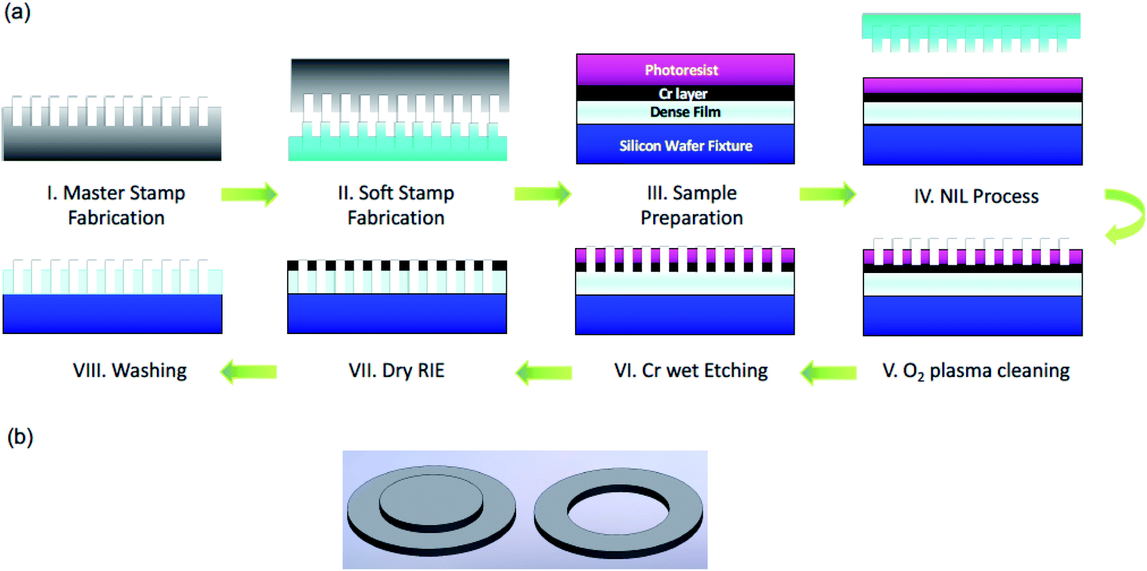 | ||
| Fig. 1 (a) NIL process step illustration; (b) silicon fixture 3D representation. | ||
2.3. Membrane characterization
3. Results and discussion
3.1. Membrane fabrication
The fabrication process starts by manufacturing the master stamp, as shown in Fig. 1(a). The design containing up to half a billion of 300 nm isopores with an identical interpore distance was transferred via e-beam lithography onto a 4-inch Si wafer which was first cleaned then deposited with the sacrificial hard mask of silicon dioxide and coated with the positive electron sensitive resist. Finally, the cavities in the master stamp were etched out with two procedures using the ICP DRIE tool. The reusable master stamp with 300 nm diameter cavities was used to create a soft stamp with 300 nm pillars by curing the PDMS solution on it via UV. Both, Si master stamp and PDMS soft stamp, were imaged by atomic force microscopy (AFM), as shown in Fig. 2a and b. Then, a 2.5 μm thick Mylar® film, as a base material, was first coated with a Cr protective layer and then fixed within the specially fabricated fixture, as illustrated in Fig. 1(b), in order to achieve a very smooth surface without any glueing material. The photoresist coated membrane system was exposed to the soft stamp through UV in the photolithographic set-up. After the oxygen cleaning and wet-etching process, the nanopores were then etched out by the dry etching procedure. In the end, the nanoporous membrane, easily extracted from the fixture, was cleaned and dried.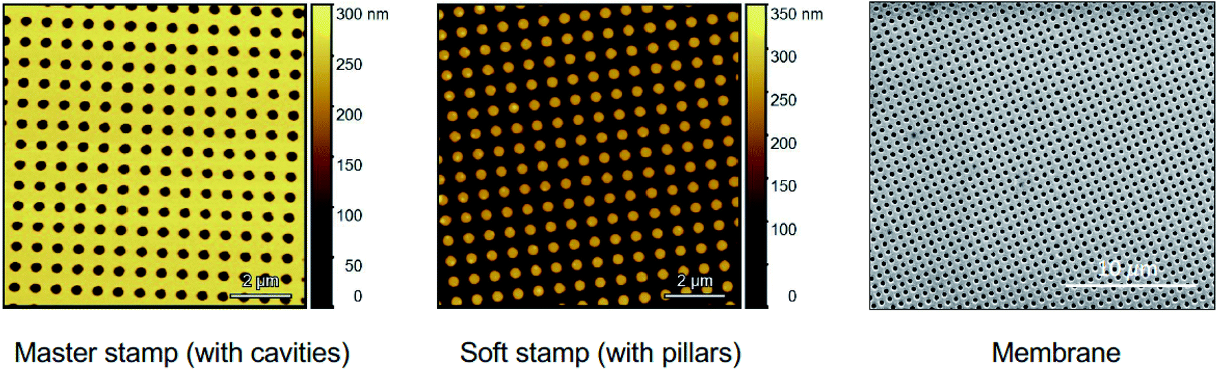 | ||
| Fig. 2 (a and b) AFM images of the (a) master stamp and (b) soft stamp; (c) SEM images of the membrane fabricated via NIL. | ||
3.2. Membrane characterization
The obtained nanoporous membrane surface was imaged by scanning electron microscopy (SEM), as shown in Fig. 2c. Highly ordered 300 nm nanopores with a similar interpore space led to a density of 4 × 10⁹ pores per cm2.The membrane permeance and rejection of particles with different sizes were investigated, as shown in Fig. 3. The water permeance measurement was performed using a stainless-steel filtration cell with an active membrane area of 1 cm2, a water feed volume of 300 mL and a trans-membrane pressure of 0.03 bar. A stable water permeance of 108000 L m−2 h−1 bar−1 was measured, as shown in Fig. 3d, which is ca. 3 to 13-fold higher than the permeation value of 38000 L m−2 h−1 bar−1 and 8500 L m−2 h−1 bar−1 obtained with the track-etched membranes with pore sizes of 400 nm and 200 nm, respectively.
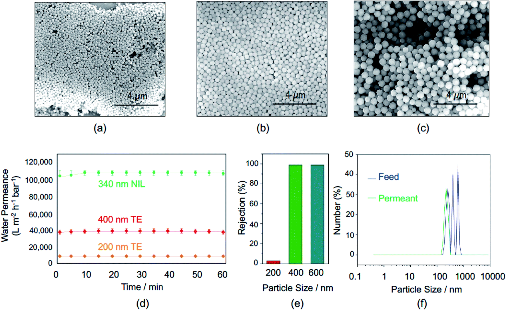 | ||
| Fig. 3 (a–c) SEM images of homogeneous ZIF-8 nanoparticles with diameters of (a) 200 nm, (b) 400 nm and (c) 600 nm; (d) water permeance of NIL and TE membranes; (e) nanoparticle rejection by the 340 nm porous NIL membranes; (f) DLS graph of mixed nanoparticles in the feed and permeant in tests with NIL membranes. | ||
In order to check the membrane rejection performance, homogeneous zeolitic imidazolate framework (ZIF) nanoparticles were synthesized with sizes of 200 nm, 400 nm and 600 nm. The ZIF-8 nanoparticle sizes were controlled by the surfactant amount added. To synthesize 200 nm sized nanoparticles, 15 mL of CTAB solution was added, while 400 nm and 600 nm nanoparticles were generated with 7 mL and 1.5 mL, respectively. Fig. 3(a–c) show the SEM images of ZIF-8 nanoparticles in different sizes.
The rejection tests were performed using dialysis glass cells. ZIF-8 nanoparticles with three different sizes were diluted in DI water separately as homogeneous mixtures and rejection tests were first performed in three separated cells. Then, a cell was used to test the sieving performance of the membrane using a heterogeneous solution with mixed 200 nm, 400 nm and 600 nm ZIF-8 nanoparticles. To see the rejection results, the feed and permeate solutions were analysed by dynamic light scattering (DLS). The graphs are shown in Fig. 3(e and f). The rejection efficiency for 400 nm and 600 nm ZIF-8 nanoparticles were as high as 100%, while for 200 nm nanoparticles it was only 3%; the membrane provides a sharp fractionation of particles in the investigated size range (Fig. 3f).
4. Conclusions
We have developed a new fabrication protocol for manufacturing an isoporous polymeric membrane with 300 nm uniform nanopores using UV-NIL, a technique combining nanopatterning and dry reactive ion etching processes. The fabricated hard master and soft PDMS stamps are reusable. The high sieving performance of the nanofabricated isoporous membrane has been demonstrated with synthesized uniform ZIF-8 nanoparticles of different sizes. The membrane with strong chemical and thermal resistances is flexible, transparent and thin (2.5 μm) making it advantageous for integration into a microfluidic device and examination of samples by optical microscopy.Author contributions
A. S. developed the membranes and performed the characterization studies. C. F. F., F. P. J., A. S. D. and U. B. assisted in the nanofabrication experiments. X. L. assisted in the nanoparticle preparation. S. P. N. supervised the project. A. S. and S. P. N. wrote the first version of the paper, which was then revised by all authors.Conflicts of interest
The authors declare no competing interests.Acknowledgements
This work was supported by the King Abdullah University of Science and Technology (KAUST).References
- F. Lyu, M. Thomas, W. Hendriks and A. Van der Poel, Anim. Feed Sci. Technol., 2020, 261, 114347 CrossRef CAS.
- A. S. Shanbhag, J. J. Jacobs, J. Black, J. O. Galante and T. T. Glant, J. Biomed. Mater. Res., 1994, 28, 81–90 CrossRef CAS PubMed.
- F. Fan and K. J. Stebe, Langmuir, 2005, 21, 1149–1152 CrossRef CAS PubMed.
- S. Wustoni, S. Wang, J. R. Alvarez, T. C. Hidalgo, S. P. Nunes and S. Inal, Biosens. Bioelectron., 2019, 143, 111561 CrossRef CAS PubMed.
- S. Zheng, H. Lin, J.-Q. Liu, M. Balic, R. Datar, R. J. Cote and Y.-C. Tai, J. Chromatogr. A, 2007, 1162, 154–161 CrossRef CAS PubMed.
- S.-J. Hao, Y. Wan, Y.-Q. Xia, X. Zou and S.-Y. Zheng, Adv. Drug Delivery Rev., 2018, 125, 3–20 CrossRef CAS PubMed.
- M. J. Tomlinson, S. Tomlinson, X. B. Yang and J. Kirkham, J. Tissue Eng., 2013, 4, 2041731412472690 Search PubMed.
- J. S. Yang, J. Y. Lee and M. H. Moon, Anal. Chem., 2015, 87, 6342–6348 CrossRef CAS PubMed.
- A. Sabirova, F. Pisig, N. Rayapuram, H. Hirt and S. P. Nunes, Sci. Rep., 2020, 10, 1–9 CrossRef PubMed.
- L. Clime, X. D. Hoa, N. Corneau, K. J. Morton, C. Luebbert, M. Mounier, D. Brassard, M. Geissler, S. Bidawid and J. Farber, Biomed. Microdevices, 2015, 17, 1–14 CrossRef CAS PubMed.
- H. Aranha-Creado, in Biotechnology, ed. C. M. W. V. L. W. K. E. Avis, CRC Press, 2020, ch. 4, pp. 167–219 Search PubMed.
- D. W. Cooper, Aerosol Sci. Technol., 1986, 5, 287–299 CrossRef CAS.
- M. Li, H. E. Muñoz, K. Goda and D. Di Carlo, Sci. Rep., 2017, 7, 1–8 CrossRef PubMed.
- E. S. Park, C. Jin, Q. Guo, R. R. Ang, S. P. Duffy, K. Matthews, A. Azad, H. Abdi, T. Todenhöfer and J. Bazov, Small, 2016, 12, 1909–1919 CrossRef CAS PubMed.
- H. Shafiee, M. B. Sano, E. A. Henslee, J. L. Caldwell and R. V. Davalos, Lab Chip, 2010, 10, 438–445 RSC.
- T. Laurell, F. Petersson and A. Nilsson, Chem. Soc. Rev., 2007, 36, 492–506 RSC.
- D. Robert, N. Pamme, H. Conjeaud, F. Gazeau, A. Iles and C. Wilhelm, Lab Chip, 2011, 11, 1902–1910 RSC.
- B. Landenberger, H. Höfemann, S. Wadle and A. Rohrbach, Lab Chip, 2012, 12, 3177–3183 RSC.
- T. Morijiri, S. Sunahiro, M. Senaha, M. Yamada and M. Seki, Microfluid. Nanofluid., 2011, 11, 105–110 CrossRef.
- X. Li, W. Chen, G. Liu, W. Lu and J. Fu, Lab Chip, 2014, 14, 2565–2575 RSC.
- J. Alvankarian, A. Bahadorimehr and B. Yeop Majlis, Biomicrofluidics, 2013, 7, 014102 CrossRef PubMed.
- P. Wilding, L. J. Kricka, J. Cheng, G. Hvichia, M. A. Shoffner and P. Fortina, Anal. Biochem., 1998, 257, 95–100 CrossRef CAS PubMed.
- V. Ramachandran and H. S. Fogler, J. Fluid Mech., 1999, 385, 129–156 CrossRef CAS.
- S. P. Nunes, Macromolecules, 2016, 49, 2905–2916 CrossRef CAS.
- M. C. Traub, W. Longsine and V. N. Truskett, Annu. Rev. Chem. Biomol. Eng., 2016, 7, 583–604 CrossRef PubMed.
- S. Sreenivasan, Microsyst. Nanoeng., 2017, 3, 1–19 Search PubMed.
- T. Glinsner, P. Hangweier, H. Luesebrink, P. Dorsey, A. Homola and D. Wachenschwanz, Solid State Technol., 2005, 48, 51–54 Search PubMed.
- S. H. Kim, K.-D. Lee, J.-Y. Kim, M.-K. Kwon and S.-J. Park, Nanotechnology, 2007, 18, 055306 CrossRef.
- C. Battaglia, J. Escarré, K. Söderström, L. Erni, L. Ding, G. Bugnon, A. Billet, M. Boccard, L. Barraud and S. De Wolf, Nano Lett., 2011, 11, 661–665 CrossRef CAS PubMed.
- E.-H. Cho, H.-S. Kim, J.-S. Sohn, C.-Y. Moon, N.-C. Park and Y.-P. Park, Opt. Express, 2010, 18, 27712–27722 CrossRef CAS PubMed.
- K. Li, K. Morton, T. Veres, B. Cui and M. Murray, in Comprehensive Biotechnology, Citeseer, 2011, pp. 125–139 Search PubMed.
- D. Xia, J. Yan and S. Hou, Small, 2012, 8, 2787–2801 CrossRef CAS PubMed.
- C.-C. Yu, K.-H. Ho, H.-L. Chen, S.-Y. Chuang, S.-C. Tseng and W.-F. Su, Biosens. Bioelectron., 2012, 33, 267–273 CrossRef CAS PubMed.
- J. D. Ryckman, Y. Jiao and S. M. Weiss, Sci. Rep., 2013, 3, 1–7 Search PubMed.
- K. Imakita, T. Kamada, M. Fujii, K. Aoki, M. Mizuhata and S. Hayashi, Opt. Lett., 2013, 38, 5067–5070 CrossRef CAS PubMed.
- S. H. Maruf, Z. Li, J. A. Yoshimura, J. Xiao, A. R. Greenberg and Y. Ding, Polymer, 2015, 69, 129–137 CrossRef CAS.
- S. T. Weinman and S. M. Husson, J. Membr. Sci., 2016, 513, 146–154 CrossRef CAS.
- Z. Ma, S. Liang, K. Xiao, X. Wang, M. Li and X. Huang, J. Membr. Sci., 2020, 612, 118332 CrossRef CAS.
- L. E. Amborski and D. W. Flierl, Ind. Eng. Chem., 1953, 45, 2290–2295 CrossRef CAS.
| This journal is © The Royal Society of Chemistry 2022 |