
 Open Access Article
 This Open Access Article is licensed under a Creative Commons Attribution-Non Commercial 3.0 Unported Licence
Assessing the electrical activity of individual ZnO nanowires thermally annealed in air†
Micka
Bah
 *a,
Taoufik Slimani
Tlemcani
*a,
Sarah
Boubenia
a,
Camille
Justeau
a,
Nicolas
Vivet
b,
Jean-Michel
Chauveau
cd,
François
Jomard
d,
Kevin
Nadaud
a,
Guylaine
Poulin-Vittrant
a and
Daniel
Alquier
*a
*a,
Taoufik Slimani
Tlemcani
*a,
Sarah
Boubenia
a,
Camille
Justeau
a,
Nicolas
Vivet
b,
Jean-Michel
Chauveau
cd,
François
Jomard
d,
Kevin
Nadaud
a,
Guylaine
Poulin-Vittrant
a and
Daniel
Alquier
*a
aGREMAN UMR 7347, Université de Tours, CNRS, INSA Centre Val de Loire, 37071 Tours, France. E-mail: micka.bah@univ-tours.fr; taoufik.slimani@univ-tours.fr; daniel.alquier@univ-tours.fr
bSTMicroelectronics Tours, 10 Rue Thalès de Milet, 37100 Tours, France
cUniversité Cote d'azur, CNRS, CRHEA, Rue B. Gregory, F-06560 Valbonne, France
dUniversité Paris-Saclay, Université Versailles-Saint-Quentin, CNRS, GEMAC, 78035 Versailles, France
First published on 12th January 2022
Abstract
ZnO nanowires (NWs) are very attractive for a wide range of nanotechnological applications owing to their tunable electron concentration via structural and surface defect engineering. A 2D electrical profiling of these defects is necessary to understand their restructuring dynamics during engineering processes. Our work proposes the exploration of individual ZnO NWs, dispersed on a SiO2/p++-Si substrate without any embedding matrix, along their axial direction using scanning capacitance microscopy (SCM), which is a useful tool for 2D carrier profiling. ZnO NWs are hydrothermally grown using 0–20 mM ammonium hydroxide (NH4OH), one of the reactants of the hydrothermal synthesis, and then annealed in a tube oven at 350 °C/1.5–15 h and 450 °C/15 h. While the as-grown ZnO NWs are highly conductive, the annealed ones exhibit significant SCM data with a high signal-to-noise ratio and temperature-dependent uniformity. The SCM signal of ZnO NWs is influenced by both their reduced dimensionality and the electron screening degree inside them. The electrical activity of ZnO NWs is only observed below a critical defect concentration that depends on the annealing temperature. Optimal SCM signals of 200 and 147 mV are obtained for samples with 0 and 20 mM NH4OH, respectively, and annealed at 350 °C/15 h. The corresponding electron concentrations of 3.27 × 10¹⁸ and 4.58 × 1018 cm−3 were estimated from the calibration curve, respectively. While thermal treatment in air of ZnO NWs is an effective approach to tune the defect density, 2D electrical mapping enables identifying their optimal electrical characteristics, which could help to boost the performance of final devices exploiting their coupled semiconducting–piezoelectric properties.
Introduction
ZnO-based nanowires (NWs) are wide direct bandgap II–VI single crystalline materials exhibiting remarkable physical properties such as semiconducting, optical, piezoelectric and ferromagnetic functionalities.1–5 ZnO-based NWs, which are lead-free and bio-compatible, play an important role as building blocks in efficient and mature nanotechnologies used for chemical–biological sensing, UV detecting and nanosystems associated with energy harvesting.6–10 Many innovative approaches are being considered to tune electron concentration levels via lattice defect engineering enabling the boosting of the multifunctional properties of ZnO NWs. The incorporation of transition metals into the ZnO lattice is an original strategy to compensate for high electron density induced by defects with holes introduced by these electron acceptors without changing the n-type conductivity. While this approach is effective to boost the thermoelectric properties of the ZnO material,11 it also offers the opportunity of pairing both ferromagnetic and semiconducting functionalities together.12 Likewise, significant effort is also devoted to the intrinsic defect level tunability and surface state modification in unintentionally doped ZnO NWs via post-synthesis annealing treatments under oxidizing or reducing atmospheres.13,14 While heat treatment in different atmospheres is an effective approach to enhance the field emission properties and UV-light emission of ZnO NWs, it is explored with the aim of shedding light on the structural defects and their origin in those single crystalline materials.15,16 Besides, both 2D imaging and good understanding of the electrical activity of these engineered structural defects along the axial or the radial direction of ZnO NWs are essential in the performance optimization of nanodevices/nanosystems. In particular, for nanogenerator devices that convert ambient mechanical energy in order to supply ultra-low power sensor nodes, the intrinsic doping level of the piezoelectric–semiconducting nanowires is the most significant parameter influencing the converted electrical energy.17,18 Determining the concentration and distribution of the free charge carriers within the NWs is a key issue in order to achieve efficient nanogenerators.19,20Electrical characterization at the nanoscale of ZnO NWs is a challenging task owing to their reduced dimensionality and large surface-to-volume ratio and also to relevant factors affecting their conductivity such as the crystalline structure, structural defects, surface states and morphology. Useful information about the electrical characteristics of individual ZnO NWs is often deduced after their integration into field effect transistors (FETs) as active channels due to their complex shapes and small characteristic size.21,22 While this innovative approach demands many technical efforts to pattern electrodes on both ends of NWs, it does not allow the 2D carrier profiling of ZnO NWs. In this context, scanning probe microscopy (SPM) techniques have emerged as powerful tools for the local electrical characterization of NWs. In the last decade, great efforts are devoted to the 2D electrical imaging of ZnO NWs using scanning capacitance microscopy (SCM) and scanning spreading resistance microscopy (SSRM).23–26 In these studies, ZnO NWs were embedded in SiO2 or polymer matrices to immobilize them and compensate for their high flexibility. The 2D electrical imaging of those upright standing NWs enabled careful investigation of the distribution of doping levels along their radial direction and at a defined time of the growth process. In the case of polymer matrices, the surrounding environment has introduced surface states that induced a p-type space charge region over a thin depth from the outer surface of the NW whereas its core does not show a SCM signal, which is indicative of high conductivity. In the case of the SiO2 matrix, a uniform SCM signal is observed along the diameter of the NW with a negligible effect of the matrix. Until now, there has been no study about electron spatial distribution along the length of ZnO NWs, which can inform on defect formation and evolution with growth time. Here, we demonstrate for the first time the feasibility of 2D carrier profiling of individual ZnO NWs along their axial direction using the SCM technique. Our strategy consists in dispersing NWs on a SiO2/p++-Si substrate, whereas the tip is moved in contact mode with a low and constant force along the length of the NW. The 2D spatial distribution of the doping concentration is then investigated as a function of annealing temperature in air ambience. We will demonstrate that ZnO NWs grown by the hydrothermal method exhibit nanoscale capacitance variations only below critical doping levels that depend on the annealing temperature.
Results and discussion
Sample description
Single n-ZnO NWs and their electrical activity are the heart of this work. To obtain well-separated ZnO NWs, they are dispersed on heavily doped p-type Si substrates on which a thermal oxide (SiO2) is grown. The use of such a SiO2/p++-Si pseudo-substrate induces a negligible effect on the SCM signal of the n-ZnO NWs. The substrate size is 1.5 × 1.5 cm2. Such an approach also allows the prevention of the mobility of the NWs beneath the tip due to huge attractive forces between n-ZnO NWs and the SiO2/p++-Si substrate. These forces originate from surface van der Waals interactions between the ZnO NW bottom facet and the SiO2 layer of the Si substrate, capillary forces arising from humidity and other interaction forces induced by the chemistry of the surfaces at the interface.27,28 Moreover, a space charge layer is formed at the contact interface when the n-ZnO and SiO2/p++-substrate are brought together, thus leading to important attractive forces between them.29The samples are grown by a hydrothermal method and exhibit a multilayer and multiscale structure as shown in Fig. 1a (see details in the Methods section). The top layer (which consists of ZnO NW arrays) is grown on a (111) – Au (gold) seed layer deposited itself on the top of a SiO2/Si substrate, which acts as a support for the first two layers. Gold was used as the template because the (111) plane of its cubic structure has a hexagonal symmetry like the (002) plane of ZnO. Such an orientation of gold promotes the c-axis orientation of the ZnO NW arrays as confirmed by the XRD pattern as shown in Fig. S1.† ESI Table 1† shows some important chemical and physical parameters used for the growth of the n-ZnO NWs (reactants, growth time and autoclave temperature). The cross-section images of the as-grown NW arrays are shown in a previous paper published by our group.22 ZnO NWs are well-ordered on the gold template and grew vertically from the Au/SiO2/Si substrate. They exhibit hexagonal faces and sharp tip shapes. The ZnO NW arrays are released from the gold layer after immersing the multilayer structure in a beaker filled with an isopropanol (IPA) solvent and sonicating the whole in an ultrasound bath for 5–10 s (see Fig. 1b). Then, NW suspension in IPA solvent is deposited on a new substrate (SiO2/p++-Si) by the drop casting method before heating the system at 90 °C/30 min to evaporate the IPA from the NW surface and contact interface (see Fig. 1c).
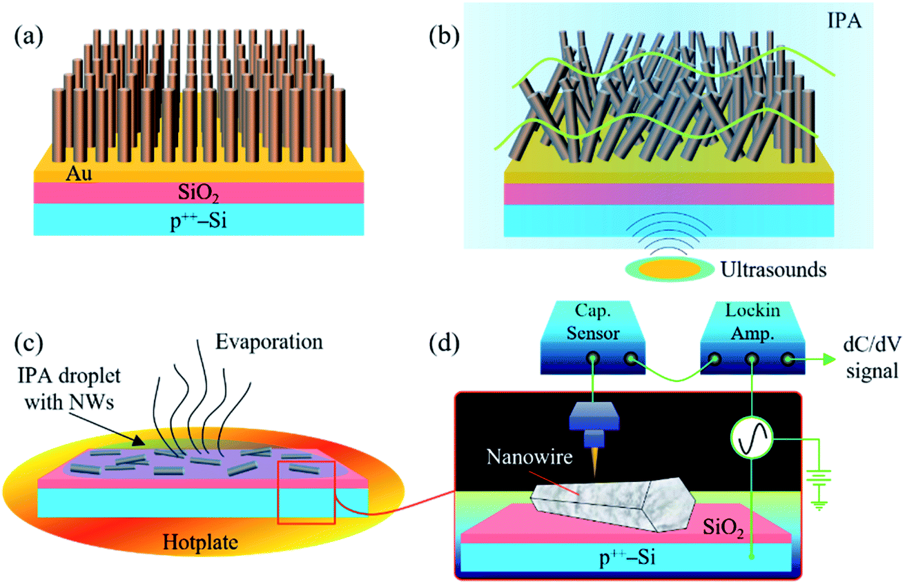 | ||
| Fig. 1 Process flow diagram for the sample preparation for SCM studies. (a) Multilayer structure showing ZnO NWs on an Au/SiO2/Si substrate. Note that the Ti layer has been omitted. (b) The NWs are detached from the Au-on-Si substrate by immersing the multilayer structure in an IPA solvent and sonicating it in an ultrasonic bath (5 to 10 s). (c) NW suspension in IPA is deposited on a heavily doped SiO2/p++-Si substrate by the drop-casting technique and IPA solvent is evaporated using a hotplate. (d) A schematic diagram of SCM measurements including a ZnO NW. The AFM tip and the NW represent locally a nanoscopic metal–semiconductor (MS) contact, thus creating a Schottky barrier. An ultra-high frequency (UHF) capacitor sensor enables capacitance variations induced by the applied bias variation to be detected and the MS capacitance is extracted from the noise thanks to the lock-in amplifier connected to the UHF sensor. The output signals of the lock-in amplifier are correlated with the amplitude and the phase of dC/dV, which informs on the concentration and the nature of the majority carriers of the semiconductor. | ||
Nanoscale capacitance-variation measurements for the different n-ZnO NWs are performed using the original experimental SCM setup shown in Fig. 1d (see details in the Methods section and in the caption of Fig. 1). In this study, the quantitative 2D carrier profiling is based on the measurement of local Schottky contact capacitance. A nanoscopic metal–semiconductor (MS) contact is formed locally when the Pt–Ir metallic probe and the ZnO NW are brought together, which induces a depletion region i.e. a capacitor due to the built-in potential in the junction. A high frequency AC bias is applied to the tip-sample structure to induce local capacitance variations due to the change of the depletion-layer width while enabling only the response of majority carriers to be recorded. The working point of the tip-sample system is found to be 0 V DC bias. The output signal of the SCM technique is the derivative of the capacitance–voltage curve (e.g. dC/dV signal) and informs on both the relative concentration and the nature (polarity) of the majority carriers. The dC/dV signal is detected thanks to an UHF capacitance sensor coupled to a lock-in amplifier. Different annealing temperatures and dwell times (350 °C/1.5 h, 350 °C/15 h and 450 °C/15 h) are selected to characterize the nanoelectrical activity of the different ZnO NWs. Hydrothermally grown ZnO NWs usually have high intrinsic defects and also hydrogen or impurity elements arising from starting materials (purity degree) can be unintentionally incorporated into the ZnO lattice during the growth process. These interrelated phenomena, which affect the doping concentrations and their spatial distribution along the NWs, and post-growth annealing treatments are expected to yield a clear difference in the nanoelectrical activity.
Nanoelectrical activity of the ZnO NWs
Fig. 2 shows the topographic (top) and SCM data (bottom) images of ZnO NWs as a function of the post-growth annealing treatment and the NH4OH concentration. Panels (A–D) and (E and F) correspond to samples prepared from batches 1 and 2 (i.e. with 0 and 20 mM NH4OH), respectively. For the data acquisition, the SCM-PTSI probe is moved in contact mode along the NW length with a constant force of 50 nN, while topography and the nanoscale capacitance variations are simultaneously acquired. As expected, attractive forces existing between the NW and SiO2/p++-Si substrate allow a stable scan over all individual NWs even after multiple passes of the tip. All probed NWs exhibit hexagonal faces and a sharp tip shape as already demonstrated using SEM imaging on the same samples in ref. 22. ZnO NWs obtained from both NH4OH concentrations have similar average diameters ϕtip ∼ 150–200 nm and ϕbase ∼ 500–600 nm and average lengths l ∼ 6–7 μm (see Fig. S2†). These dimensions in the radial direction (i.e. ϕtip and ϕbase) can be of major concern in particular at low doping concentration, where they become inferior or equal to the Debye screening length in ZnO (see Fig. S3†). This may thus affect the SCM spatial resolution, which depends on the strength of electron screening, measured from the Debye screening length. Besides, before SCM measurements, a SRAM normalized test sample is used to set the lock-in amplifier and to define the polarity of the SCM data. This procedure also enables verifying that the SCM technique is working correctly. Furthermore, a few NWs are measured before and after annealing to ensure that no artifacts are present. More precisely, most of the measurements (not shown here) are made on the as-grown NWs to confirm that they are strongly conductive. To highlight the reproducibility of the SCM measurements, a comparison between two NWs, obtained with 20 mM NH4OH and annealed at 350 °C/15 h, is shown in Fig. S4.† In addition, SCM signals from NWs obtained from 0 and 20 mM NH4OH and annealed at 350 °C/15 h or 450 °C/15 h, as Fig. 2 shows, provide additional statistical information to validate the measurements. | ||
| Fig. 2 Effect of post-growth annealing treatment on the electrical activity of solution-processed ZnO NWs determined using scanning capacitance microscopy. Post-growth annealing treatment promotes crystallinity and lowers the defect density in the ZnO NW, which is beneficial for carrier transport modulation. Topography and capacitance variation images are simultaneously acquired enabling a real-time correlation between local topography and spatial resolution. Topography (top, units in nm) and SCM data (bottom, units in mV) images are those for batch 1 (samples A–D) and for batch 2 (samples E and F). Sample (A): as-grown, sample (B): annealed at 350 °C/1.5 h, samples (C) and (E): annealed at 350 °C/15 h and samples (D) and (F): annealed at 450 °C/15 h. Sample series (A–D) and (E and F) are grown with the addition of 0 and 20 mM NH4OH in the growth solution, respectively. Scale bar corresponds to 500 nm. | ||
Let's consider the SCM images from panels (A)–(D). Except the un-annealed sample (A), all other samples (B–D) exhibit significant SCM data with the maximum dC/dV signal for sample (C), annealed at 350 °C/15 h. It is worth noticing that nanoelectrical activity is only observed below a critical doping concentration that depends on the annealing temperature. Indeed, the free charge carrier density in ZnO NWs can be modulated by tuning intrinsic point defects and modifying the surface states thanks to annealing treatments.30,31 Hydrothermally grown ZnO NWs usually have many lattice and surface defects associated with oxygen vacancies or zinc interstitials and various surface adsorbates.32,33 Moreover, hydrogen originating from reactants and also impurities initially present in the starting materials (purity of 98%) may be unintentionally incorporated into the ZnO lattice, thus leading to a large doping concentration in the as-grown ZnO NWs. Unannealed NWs appear naturally highly conductive, which induces a low Schottky barrier between the Pt–Ir coated probe and the NW. As a result, the depletion layer beneath the tip becomes extremely thin and current tunnels through it due to the high conductivity of the NW. Therefore, the local capacitance variations get negligible. This is the case for sample (A). Otherwise, when the NW is annealed in ambient air, the predominant mechanism at its surface is the chemisorption of oxygen related molecules. These latter capture free charge carriers from the interior of the NW thus acting as electron acceptors, which enables the doping concentration to be modulated without changing the n-type conductivity of the NW. This charge transfer varies exponentially with increasing temperature,34 and also induces an upward band bending at the NW surface.35 This decrease in carrier concentration is responsible of the appearance of SCM data shown in panels (B)–(D).
The non-uniformity of the signal for the sample (B) (i.e. 350 °C/1.5 h) is probably due to the difference in doping concentration between the base and the tip of the NW, which results in the change of the Debye screening length and thus of the SCL thickness beneath the probe. Increasing the annealing temperature to 350 °C/15 h (sample C) or 450 °C/15 h (sample D) leads to a more homogeneous carrier distribution by defects reducing and restructuring along the length of the NWs and is consistent with the uniform SCM data observed on the top facet. The sample series (E) (350 °C/15 h) and (F) (450 °C/15 h) (obtained with NH4OH) display similar trends to samples (C) and (D) and their differences will be discussed in the following section. It is worth mentioning that the background dC/dV signal (i.e. that of the p++-Si substrate) is very low and does not significantly affect those of ZnO NWs. The sign of the SCM data is negative, indicating that all the ZnO NWs are of n-type, which is consistent with the nature of unintentionally doped ZnO, while its amplitude gives information about the doping concentration.
As can be seen in panels (A)–(D) and (E and F) of Fig. 2, the 2D SCM data are not uniform along the radial direction of all individual NWs regardless of the annealing temperature. To assess the nanoelectrical activity profile across the NW radial direction, we show in Fig. S5† the 1D SCM signal along the NW radial depth. The dC/dV signal across the radial direction shows an oscillating spectrum for all NWs with both SCM spikes on the edge facets. A schematic representation of this derivative capacitance–voltage profile shown in Fig. 3A is proposed to understand the origin of this oscillating behavior. While the top facet exhibits a constant and stable profile over a certain depth, the dC/dV signal decreases substantially when the probe approaches the border between two neighboring facets before increasing again on edge facets. First, the signal drop is due to the decrease in the probed surface, which alters the skin depth of the depletion layer and reduces the spatial resolution. Second, the signal increase on the edge facets may be due to two interrelated phenomena. Edge facets can be assimilated to a 60°-beveled surface as schematized in Fig. 3B. More precisely, the edge facet acts as a small portion of the top facet, which is increased by a factor of 2/√3 along the radial direction as in the case of a sample prepared in the configuration of angle beveling.36 In this context, the spatial resolution will increase by 2/√3 relative to that of the top facet. The other contribution can be associated with the increase in the tip-sample contact surface, which may also enhance the measured dC/dV signal (see Fig. 3C). Otherwise, when the tip scans over the top facet of the NW, the tip-sample contact surface remains constant (see Fig. 3D) due to the low roughness and flat surface. Assuming that the doping concentration is uniform along the length of the NW, the spatial resolution that depends on the lateral extension of the depletion region beneath the tip will remain unchanged over its top facet. All these effects explain the observed SCM signal of the different NWs and only that of the top facet is free of artefacts. For that reason, only the dC/dV signal on the top facet along the length of the NW can be considered for a precise quantitative determination of the doping concentration.
 | ||
| Fig. 3 Nanoelectrical profile evidencing a change in spatial resolution along the NW radial direction. (A) Contour plot of the SCM signal across the NW radial direction, (B) influence of the side facet tilt, which acts as a beveled surface, (C) variation of the tip-sample contact surface on the side facet and (D) constant tip-sample contact surface on the top facet. | ||
To show the evolution of the electrical activity, we plotted in Fig. 4A and B the dC/dV signal profile of the top facet (excluding the border signal) along the length of the NW as a function of the annealing temperature for the sample series (A)–(D) and (E and F). While sample (A) (as grown) exhibits no capacitance variations due to its high conductivity, the dC/dV signal emerges from the SCM noise for sample (B) (350 °C/1.5 h), and then reaches a maximum value of −200 mV for sample (C) (350 °C/15 h) before falling to −120 mV for sample (D) upon increasing the annealing temperature to 450 °C/15 h (see Fig. 4A). Samples (E) (350 °C/15 h) and (F) (450 °C/15 h) exhibit SCM data values of −150 mV and −90 mV, respectively (see Fig. 4B). First, the dC/dV signal profile for both sample series (i.e. (A)–(D) without and (E and F) with NH4OH) show the same evolution versus post-growth annealing temperature. Second, for an equivalent temperature, the dC/dV signals for the sample series (E and F) are lower than those of the sample series (C and D). This result provides evidence that the use of NH4OH introduces additional lattice defects into hydrothermally grown ZnO NWs. The fact that the electrical activity increases and then decreases with increasing annealing temperature involves the influence of the spatial resolution, which itself depends on the intensity of doping via the screening length inside the NW. The applied voltage and the screening effect set the shape and the depth of the tip-induced depletion layer and define the resolution of the measurement.37 Due to its one-dimensionality, the NW radial dimension becomes very close to the Debye screening length at a low doping level and, as already proved by Johnson et al.,38 the tip-induced space-charge layer cannot be defined to be better than a few Debye screening lengths. Thus, the SCM technique can resolve changes in carrier concentrations only within this degree of accuracy. This explains why the samples annealed at 450 °C/15 h (which have reduced doping levels) show lower SCM data than those annealed at 350 °C/15 h due to this limiting effect in the spatial resolution, as they are probably completely depleted of free charge carriers in their radial direction. Very recently, Casper et al.39 reported a similar phenomenon on Si NWs from sequential finite element simulation studies.
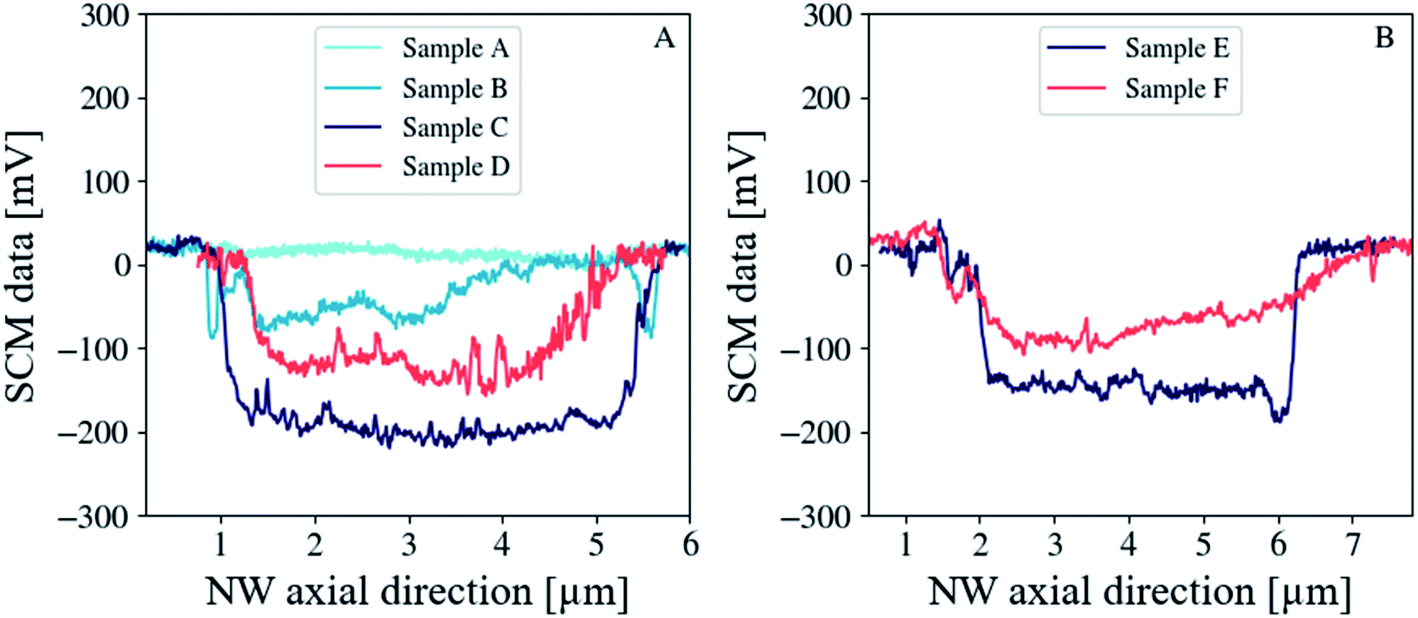 | ||
| Fig. 4 Electrical activity along the axial direction of individual ZnO NWs annealed at various temperatures. The dC/dV response becomes clear and shows a high signal-to-noise ratio with increasing annealing temperatures. (A) Sample (A) (as-grown) displays no capacitance variations due to its high conductivity, while annealed ones (i.e. samples B–D) show progressively capacitance evolutions due to the lattice defects reducing and restructuring inside individual NWs. (B) Sample series (E and F) (obtained with the NH4OH additive) show a similar behavior to the sample series (C and D), respectively. Their lower signal than that of samples (C and D) confirms that the use of NH4OH introduces additional defects into the ZnO lattice. | ||
Quantitative SCM measurements of annealed ZnO NWs
The n-type ZnO calibration sample used for the quantitative SCM measurements exhibits a multilayer structure as shown in Fig. 5 (see details in the caption). It consists of two sets of (Zn,Ga)O stripe series positioned next to each other and separated by (Zn,Mg)O layers (with a residual doping density below 1016 cm−3). The gray to dark stripes in Fig. 5a correspond to the uniformly Ga doped layers, while the light blue ones represent the Mg doped stripes. The use of (Zn,Mg)O layers allows the precise determination of the thicknesses in STEM thanks to the chemical contrast generated by the atomic difference. In Fig. 5b, the (Zn,Mg)O layers (light stripes) and (Zn,Ga)O layers (dark stripes) can be clearly seen from the STEM image, thus evidencing the multilayer structure. Moreover, adding Mg into unintentionally doped ZnO reduces further the residual doping.40 Each set is formed from nine doped stripes (including the central doped layer) with Ga doping concentrations monotonically increasing from 1.5 × 10¹⁷ to 5 × 1020 cm−3. For SCM investigations, an n-type staircase ZnO sample is prepared in the cross-section configuration. The AFM deflection error signal (see Fig. 5c), which is sensitive to the material boundaries, enables the area of interest (doped and separator layers) to be identified while the SCM signal shown in Fig. 5d informs on the electrical activity of the active nano-regions. First, (Zn,Ga)O and (Zn,Mg)O stripes are well contrasted due to their difference in the degree of electron screening or doping levels. More precisely, the SCM signal is inversely proportional to the doping concentration meaning that (Zn,Ga)O layers will appear lighter than the (Zn,Mg)O ones. Second, the highly doped (Zn,Ga)O layers in the central region are well resolved compared to the lightly doped ones on the sample edges. This weak contrast between Mg and Ga doped layers on the ZnO calibration sample edges may be due to lower Ga concentration. Indeed, the spatial resolution of the doped layers decreases progressively with decreasing [Ga] and becomes very close (not exactly the same values) to that of the Mg doped stripes. This is due to the increase in the lateral extension of the depletion region beneath the tip, which modulates the spatial resolution. | ||
| Fig. 5 Quantitative SCM measurements. (a) Schematic view of the staircase structure. Gray to dark stripes are the uniformly doped (Zn,Ga)O layers, while the light blue ones correspond to the (Zn,Mg)O layers. (b) STEM image of the ZnO calibration sample. Dark and light stripes of the STEM image correspond to (Zn,Ga)O and (Zn,Mg)O layers, respectively. The (Zn,Ga)O and (Zn,Mg)O stripes with an average thickness of 86 nm and 50 nm are grown on an ∼400 nm ZnO buffer layer. The Ga doping concentration monotonically increases from 1.5 × 10¹⁷ to 5 × 1020 cm−3, while the (Zn,Mg)O layers have a residual doping level below 1016 cm−3.41 (c) Deflection error image arises from the difference between the cantilever deflection setpoint and feedback signal of the AFM and gives information about boundaries between the different nano-regions. (d) SCM data image of the calibration sample informs on the doping level of the different stripes. | ||
To assess the different Ga doping levels of the staircase structure, both the SCM data (acquired with VAC = 3000 mV and VDC = 0 V) and the SIMS versus depth profiles are superimposed as Fig. 6a shows. The SCM data profile exhibits multiple spikes, whose minima correspond to the different Ga doping levels. The (Zn,Mg)O layers show a high SCM data amplitude due to their low residual doping levels. While the SIMS versus depth profile exhibits rectangular boxes for the different doped layers, the SCM one presents a smoother contour plot. This behavior for the SCM signal is associated with the change in spatial resolution due to large gradients of doping at the (Zn,Ga)O/(Zn,Mg)O interfaces. More precisely, the spatial resolution, which attains necessary few Debye screening lengths (function of doping concentration), induces a tip-average effect near these gradients. This phenomenon occurs in almost all staircase samples with the SCM technique and can be overcome by angle beveling.42 For the precise usage of the SCM profile, only data from the middle-doped layers are extracted for the calibration curve construction. Besides, a good agreement between the SCM signal and the SIMS profile versus depth is observed demonstrating the capability of the SCM technique to profile carrier concentration over a wide dynamic range of 5 × 10¹⁷ to 5 × 1020 cm−3 for the ZnO nanostructures.
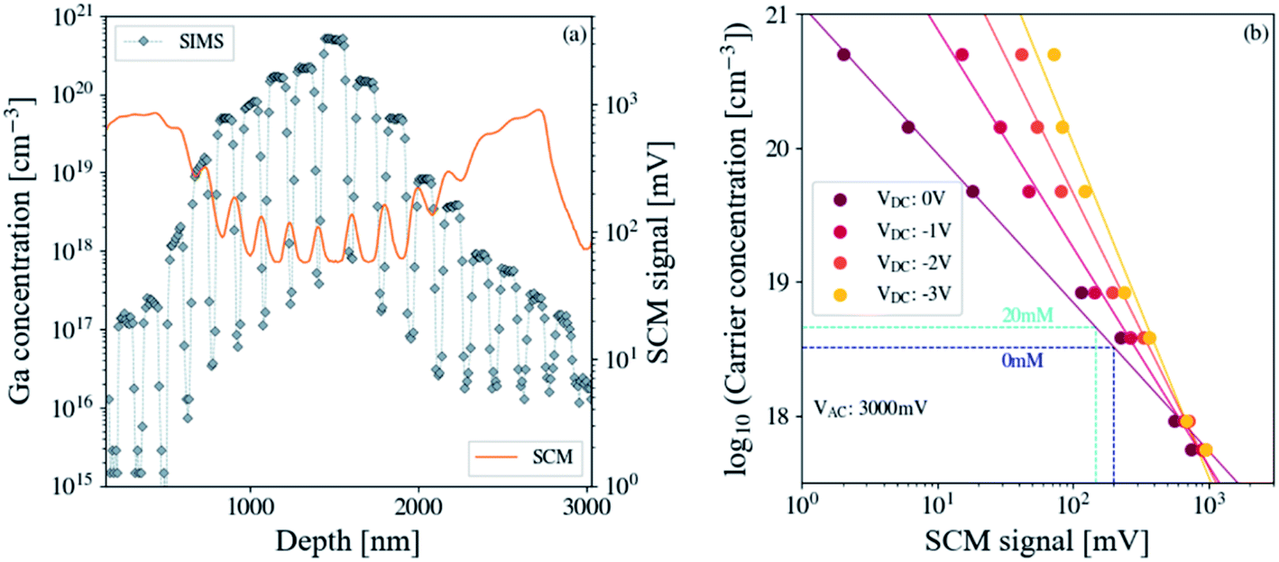 | ||
| Fig. 6 Calibration curves for the SCM signal conversion into doping concentration. (a) SCM is an electrical profiling technique while SIMS is a chemical profiling one. They are complementary techniques and superimposing their profile allows the conversion of the SCM signal into doping density. (b) Ga concentrations versus SCM data calibration curves for a set of DC biases ranging from 0 to −3 V: filled circles correspond to experimental values (minima of the SCM data and corresponding [Ga] in (a)) and solid lines are the linear fits of these experimental data. | ||
Fig. 6b shows the semi-log plot of the experimental Ga doping concentration versus SCM signal calibration curves obtained for a set of DC biases ranging from 0 to −3 V. These data are extracted from the first set of nine doped stripes adjoining the ZnO substrate. To lighten the discussion and for simplicity, the other set will not be addressed here. Besides, the SCM signal monotonically decreases with the set of monotonically rising Ga concentration levels previously reported. These results evidence that monotonic calibration curves can be reached for a set of DC biases in the range from 0 to −3 V for the ZnO calibration sample in the absence of contrast reversal for the lowly doped layers. The dynamic range of the SCM data i.e. the voltage difference between the lowest and the highest Ga doping concentration is 0.8–0.9 V. For the quantitative SCM data conversion into units of doping concentrations, the NWs and the calibration sample are measured under the same experimental conditions; more precisely, the same tip, deflection force and high frequency AC and DC biases are used for a unique AFM session. We also assume that the Ga atoms are totally ionized and electron concentrations are equivalent to the donor doping ones (i.e. [Ga]).43 Otherwise, as already addressed above, the SCM data of ZnO NWs annealed at 350 °C/1.5 h (sample (B) with 0 mM NH4OH) and 450 °C/15 h (samples (D) and (F) with 0 mM and 20 mM NH4OH, respectively) are not optimal due to the dopant inhomogeneity along the axial direction of the NW for the former and reduced spatial resolution for the latter. Note that the as-grown NW does not exhibit SCM data due to its high conductivity (sample (A) with 0 mM NH4OH). However, ZnO NWs annealed at 350 °C/15 h (samples (C) and (E) with 0 mM and 20 mM NH4OH, respectively) show a good compromise between the spatial resolution and doping uniformity and are suitable for the SCM data conversion. SCM data intensity for ZnO NWs corresponding to 0 and 20 mM NH4OH is equal to 200 and 147 mV, respectively. Their projection on the calibration curve (for VAC = 3000 mV and VDC = 0 V) shows that the carrier concentration increases from 3.27 × 10¹⁸ to 4.58 × 1018 cm−3 when the NH4OH one varies from 0 to 20 mM. These results confirm that the addition of NH4OH introduced some extra defects into the ZnO NWs.
Table 1 summarizes the carrier concentration of annealed ZnO NWs with respect to growth techniques and characterization approaches. Growth methods strongly influence the doping level in ZnO NWs. From a general standpoint, solution growth techniques (hydrothermal growth, chemical bath deposition, electrodeposition, etc.) seem to result in higher doping levels than vapor phase methods (molecular beam epitaxy and vapor deposition). This discrepancy probably originates from the difference in unintentional dopants, initially present in the starting materials coupled to diffusion mechanisms and growth temperature/pressure, incorporated in the final product. Although the carrier concentration of the as-grown ZnO NWs is not known due to their high conductivity, our post-annealing data obtained from SCM are in good agreement with those previously reported from electrochemical impedance, FETs, Hall effect, scanning near-field optical microscopy and SCM measurements (see Table 1). More significantly, our 2D electrical profile images provide direct evidence that, for the first time, free-carrier charges are non-homogeneously distributed along the axial direction of n.i.d ZnO NWs for low annealing time, which can also be expected for the as-grown ones. In fact, the progressive decrease of nutrients present in solution, as the hydrothermal growth progresses, can probably induce a gradient of the doping level along the growth axis of ZnO NWs. However, when increasing the annealing time, free-carrier charges are uniformly redistributed through the diffusion process in the solid phase. While 2D profiling techniques such as SCM and s-SNOM are applied to embedded upstanding n.i.d ZnO NWs in specific matrices and revealed doping inhomogeneity along their radial direction,25,50 at present, the doping heterogeneity and spatial redistribution of free-carrier charges along their axial direction thanks to annealing treatment are demonstrated.
| Carrier concentration (cm−3) | Growth techniques | Characterization means | Annealing | Reference |
|---|---|---|---|---|
| 2.40 × 10¹⁸ | VLS mechanism | FETs | Laser: 100 mJ cm−2 | 44 |
| 3.97 × 10¹⁷ | MBE | Hall effect | 600 °C/1 h/O2 | 45 |
| 5.20 × 10²⁰ | HTG | Hall effect | 350 °C/1 h/air | 46 |
| 1.00 × 10¹⁷ | VD method | EIS | 400 °C/1 h/O2 | 47 |
| 1.60 × 10¹⁸ | Electrodeposition | EIS | 450 °C/1 h/air | 48 |
| 1.70 × 10¹⁹ | AS method | EIS | 350 °C/1 h/O2 | 49 |
| <1018 | Electrodeposition | s-SNOM | 450 °C/1 h/air | 50 |
| 5.00 × 10¹⁷ to 2 × 10¹⁸ | CBD | SCM | As-deposited | 51 |
| 3.27–4.58 × 10¹⁸ | HTG | SCM | 350 °C/15 h/air | This work |
Otherwise, Shi et al. have demonstrated from first principles calculations that the electron concentration for optimal thermoelectric performance of ZnO NWs must be in the range from ∼1018–1019 cm−3.52 Our work demonstrates, thanks to the 2D electrical imaging tool, that defect levels in hydrothermally grown ZnO NWs carefully thermally treated at convenient temperature can fall in this range. This strategy may also lead to a new design methodology to boost the performance of ZnO nanogenerators via efficient coupling between semiconducting and piezoelectric properties. By decreasing the free charge carrier concentration, the screening of piezoelectric charges should be lowered, and the piezopotential produced by the nanogenerator is expected to increase.17–19
Methods
ZnO NW synthesis
Before the growth of ZnO NWs, a 500 μm thick silicon wafer (100) with a surface area of 2 × 2 cm2 is cleaned through sequential washes in a mixture of sulfuric peroxide (H2SO4![[thin space (1/6-em)]](https://www.rsc.org/images/entities/char_2009.gif) :H2O2, 1:1), diluted hydrofluoric acid (HF-25%) and deionized (DI) water. This cleaning process is previously described within our team by Tlemcani et al.53. Next, a thin adhesive titanium layer (100 nm) is DC sputtered at room temperature on the top surface of silicon samples (power of 500 W and pressure of 5 mTorr) under an argon atmosphere followed by 200 nm gold layer deposition. Afterward, ZnO NW arrays are grown on the surface of the gold layer via a low temperature hydrothermal method. As summarized in ESI Table 1,† the precursor chemicals employed for the ZnO NW growth included zinc nitrate hexahydrate Zn(NO3)2·6H2O (98%), hexamethylenetetramine (HMTA) (CH2)6N4 (>99.5%) and ammonium hydroxide NH4OH (29%) solution. The growth is carried out in a stainless steel autoclave reactor, in which two equimolar stock solutions of precursors (Zn(NO3)2 and HMTA) are mixed including the addition of ammonia solution, where its concentration is varied from 0 to 20 mM. After hermetically sealing the autoclave, it is placed in a preheated convection oven for 15 h at 85 °C. The entire procedure is previously described in detail in our group by Boubenia et al.22
:H2O2, 1:1), diluted hydrofluoric acid (HF-25%) and deionized (DI) water. This cleaning process is previously described within our team by Tlemcani et al.53. Next, a thin adhesive titanium layer (100 nm) is DC sputtered at room temperature on the top surface of silicon samples (power of 500 W and pressure of 5 mTorr) under an argon atmosphere followed by 200 nm gold layer deposition. Afterward, ZnO NW arrays are grown on the surface of the gold layer via a low temperature hydrothermal method. As summarized in ESI Table 1,† the precursor chemicals employed for the ZnO NW growth included zinc nitrate hexahydrate Zn(NO3)2·6H2O (98%), hexamethylenetetramine (HMTA) (CH2)6N4 (>99.5%) and ammonium hydroxide NH4OH (29%) solution. The growth is carried out in a stainless steel autoclave reactor, in which two equimolar stock solutions of precursors (Zn(NO3)2 and HMTA) are mixed including the addition of ammonia solution, where its concentration is varied from 0 to 20 mM. After hermetically sealing the autoclave, it is placed in a preheated convection oven for 15 h at 85 °C. The entire procedure is previously described in detail in our group by Boubenia et al.22
ZnO staircase structure growth
The staircase structure is grown by plasma assisted molecular beam epitaxy on a 10 × 20 mm m-oriented ZnO substrate. Before growth, the substrate is annealed at 1065 °C under an oxygen (O) atmosphere to evidence the atomic steps, while the substrate temperature is set to 420 °C during growth. The atomic O is provided by a plasma cell operating at 320 W and the O flow is fixed at 1 sccm. The Zn (Mg) and O fluxes are adjusted to be close to stoichiometry to minimize defect concentrations with a growth rate of 300 nm h−1. The n-type doping is provided by a Ga cell whose temperature is varied to obtain the staircase profile. The structure consists of a 400 nm ZnO buffer layer, on which a series of 17 layers of Ga doped ZnO (from 1017 to 5 × 1020 cm−3) separated by a 50 nm (Zn,Mg)O stripe series are deposited. The Mg content and the global (Zn,Mg)O thicknesses are defined so as to prevent strain relaxation, which is highly anisotropic in non-polar orientations ([Mg] ∼ 10%). Further details are available in ref. 54 and 55. To confirm the multilayer structure of the calibration sample, a thin lamella has been prepared using the standard in situ lift-out procedure.56 A dual-beam FIB-SEM equipment (FEI Strata DB 400-S) has been used for such sample preparation and also for the scanning transmission electron microscopy (STEM) inspection at 30 keV.SIMS analysis of the staircase structure: determination of the gallium doping concentration
Dynamic SIMS experiments are performed using a CAMECA IMS7f instrument. O2+ ions are used as primary ions with an effective energy of 5 keV and an incidence angle of ∼52°. The primary beam is scanned over 150 × 150 μm2, while the primary current is adjusted to 20 nA. Secondary ions are detected in the positive mode and collected from an area of 33 μm in diameter, centred in the sputter crater. After having verified that no mass interference occurs at 69 u.m.a. (69Ga), the experiment is done at low mass resolution (M/ΔM = 300). Assuming a constant sputtering rate over the profile duration, the conversion of the sputtering time (s) to the depth (nm) is done thanks to the measurement of the depth crater with a Dektak 8 stylus profilometer. From the gallium profile, the intensity detected in count per second (cps) is converted to concentration (at cm−3) thanks to calibrating SIMS data through a ZnO standard implanted with 69Ga (a nominal dose of 1.0 × 10¹⁵ at cm−2). Therefore, the absolute accuracy of the gallium SIMS profile is expected to be around 10%.Scanning capacitance microscopy (SCM)
SCM measurements are performed using a Bruker Dimension Icon AFM apparatus equipped with a Nanoscope V controller. The SCM technique is a useful tool dedicated to the 2D electrical profiling of carrier concentration in semiconductor devices, especially at material interfaces.57 The SCM experimental setup includes an AFM conductive probe, ultra-high frequency (∼1 GHz) capacitance sensor, lock-in amplifiers, multi-channel signal processing systems and 2D map plotters. The relevant parameters for SCM are the spatial resolution (which depends on the lateral extension of the depletion region beneath the tip), the DC bias, the high frequency (∼90 kHz) AC bias, the scan rate (usually 0.25 Hz) of the AFM tip, the insulator quality, the surface roughness and the backside contact. In typical SCM measurements, the metallic tip is moved in contact mode while the local metal–insulator–semiconductor (MIS) structure is excited by a DC bias superimposed on a high-frequency AC bias. High-frequency AC bias enables the majority carriers to be periodically accumulated near the insulator–semiconductor interface and repelled from the interface, while DC bias ensures that the system works around its operating point. In this work, an AC bias set to 3000 mV and a DC bias to 0 V are applied to the sample, while the tip is grounded. A heavily doped crystalline Si tip coated with a thin metallic film of Pt–Ir (SCM-PTSI), which has a nominal tip radius of curvature of 15 nm, is employed for the 2D carrier profiling of the single ZnO NW.Sample preparation
Low temperature solution grown ZnO NWs usually contain huge structural and surface defects making them highly conductive. It is worth mentioning that our NWs exhibit high crystal quality (see Fig. S1†). These defects can be modulated via defects reducing and restructuring by post-synthesis thermal treatments. The aim of this work is to study the effect of post-growth annealing treatment on the 2D electrical activity of solution-processed ZnO NWs using scanning capacitance microscopy. For that purpose, the hydrothermally grown ZnO NW arrays are released separately in IPA solution from substrate no. 1 (i.e. batch 1: 0 mM NH4OH) and substrate no. 2 (i.e. batch 2: 20 mM NH4OH) using an ultrasonic bath for 5 to 10 s. The NW suspension in IPA from batch 1 is deposited by the drop-casting method on 4 new SiO2/p++-substrates with a surface area of 1.5 × 1.5 cm2, referred to as samples (A)–(D). Sample (A) is taken as the control sample (i.e. unannealed sample), while samples (B)–(D) are thermally treated at 350 °C/1.5 h, 350 °C/15 h and 450 °C/15 h under air in a horizontal quartz tube furnace, respectively. The NWs from batch 2 are divided into samples (E) and (F) and are annealed at 350 °C and 450 °C/15 h, respectively. In the final step, each sample is glued to a metallic chuck with conductive silver paste for AFM electrical studies.Conclusion
Hydrothermally grown ZnO NWs are individually characterized along their axial direction using scanning capacitance microscopy. A SiO2/p++-Si substrate enables ZnO NWs to be stabilized due to attractive forces existing between them at their interface. The 2D electrical imaging of the NWs reveals that their SCM response is influenced by the Debye screening length, which depends on the doping level itself modulated by annealing treatment at different temperatures. While the as-grown NWs are highly conductive, the annealed ones show significant SCM data, which appears at a critical doping level related to annealing temperature. The optimal value of the SCM signal is obtained at 350 °C/15 h due to a good spatial resolution that is controlled by the lateral expansion of the depletion region beneath the tip. We highlight that the SCM signal of ZnO NWs decreases at 450 °C/15 h owing to their low doping levels that increase the screening length and give rise to the complete depletion of NWs along their radial direction. Moreover, the addition of NH4OH in the growth solution introduces extra defects into the ZnO lattice resulting in a reduced SCM signal. Indeed, the doping concentration estimated from the experimental calibration curve increases from 3.27 × 10¹⁸ to 4.58 × 1018 cm−3 when the NH4OH level varies from 0 to 20 mM, respectively. This study enables the optimal electrical activity of ZnO NWs to be identified, which paves the way for boosting the performance of ZnO nanogenerators via efficient coupling between semiconducting and piezoelectric properties.Author contribution
The strategy adopted for this work is defined and conceived by S. B., C. J., T. S. T., M. B., K. N., G. P.-V. and D. A.; S. B., C. J. and T. S. T. synthesized the different ZnO NW array samples; J.-M. C. grew the ZnO calibration sample and N. V. performed the STEM characterization of this sample; F. J. performed the SIMS measurements; M. B. and T. S. T. performed the SCM measurements; M. B. performed the data processing, designed the figures, and wrote the majority of the manuscript; T. S. T., J.-M. C. N. V., K. N., G. P.-V. and D. A. contributed to the writing of the manuscript and to the discussion of the results; K. N., G. P.-V. and D. A. did critical review of the manuscript; all authors have read and approved the manuscript.Conflicts of interest
The authors declare that there are no conflicts of interest.Acknowledgements
This research was funded by the EnSO project through the electronic components and systems for European leadership joint undertaking in collaboration with the European Union’s H2020 framework programme (H2020/2014–2020) and national authorities (grant agreement number 692482). This work was also funded by the EU commission under the H2020 FET-OPEN program; project “ZOTERAC” FET-OPEN 6655107. The authors thank V. Sallet (GEMAC) for SIMS measurements and D. Lefebvre (CRHEA) for technical contribution to MBE growth.References
- M.-P. Lu, J. Song, M.-Y. Lu, M.-T. Chen, Y. Gao, L.-J. Chen and Z. L. Wang, Nano Lett., 2009, 9, 1223–1227 CrossRef CAS PubMed.
- R. Ben-Zvi, O. Bar-Elli, D. Oron and E. Joselevitch, Nat. Commun., 2021, 12, 3286 CrossRef CAS PubMed.
- Z. L. Wang and J. Song, Science, 2006, 312, 242–245 CrossRef CAS PubMed.
- C. Justeau, T. S. Tlemcani, G. Poulin-Vittrant, K. Nadaud and D. Alquier, Materials, 2019, 12, 2511 CrossRef CAS.
- D. Wang, Q. Chen, G. Xing, J. Yi, S. R. Bakaul, J. Ding, J. Wang and T. Wu, Nano Lett., 2012, 12, 3994–4000 CrossRef CAS PubMed.
- X. Zhou, A. Wang, Y. Wang, L. Bian, Z. Yang, Y. Bian, Y. Gong, X. Wu, N. Han and Y. Chen, ACS Sens., 2018, 3, 2385–2393 CrossRef CAS PubMed.
- A. Choi, K. Kim, H.-I. Jung and S. Y. Li, Sens. Actuators, B, 2010, 148, 577–582 CrossRef CAS.
- Y. Zhang, T. R. Nayak, H. Hong and W. Cai, Curr. Mol. Med., 2013, 13, 1633–1645 CrossRef CAS PubMed.
- C. Soci, A. Zhang, B. Xiang, S. A. Dayeh, D. P. R. Aplin, J. Park, X. Y. Bao, Y. H. Lo and D. Wang, Nano Lett., 2007, 7, 1003–1009 CrossRef CAS PubMed.
- T. S. Tlemcani, C. Justeau, K. Nadaud, D. Alquier and G. Poulin-Vittrant, Nanomaterials, 2021, 11, 1433 CrossRef CAS PubMed.
- H. Ahmoum, G. Li, S. Belakry, M. Boughrara, M. S. Su'ait, M. Kerouad and Q. Wang, Mater. Sci. Semicond. Process., 2021, 123, 105530 CrossRef CAS.
- Z.-B. Gu, M.-H. Lu, J. Wang, D. Wu, S. T. Zhang, X. K. Meng, Y.-Y. Zhu, S.-N. Zhu and Y. Chen, Appl. Phys. Lett., 2006, 88, 082111 CrossRef.
- L.-H. Quang, S. J. Chua, K. P. Loh and E. Fitzgerald, J. Cryst. Growth, 2006, 287, 157–161 CrossRef CAS.
- M. Li, G. Xing, L. F. N. Ah Qune, G. Xing, T. Wu, C. H. A. Huan, X. Zhang and T. C. Sum, Phys. Chem. Chem. Phys., 2012, 14, 3075–3082 RSC.
- V. Quemener, L. Vines, E. V. Monakhov and B. G. Svensson, Int. J. Appl. Ceram. Technol., 2011, 8, 1017–1022 CrossRef CAS.
- W. Mtangi, F. D. Auret, W. E. Meyer, M. J. Legodi, P. J. J. Van Rensburg, S. M. M. Caelho, M. Diale and J. M. Nel, J. Appl. Phys., 2012, 111, 094504 CrossRef.
- C. Opoku, A. Dahiya, F. Cayrel, G. Poulin-Vittrant, D. Alquier and N. Camara, RSC Adv., 2015, 5, 69925–69931 RSC.
- O. Graton, G. Poulin-Vittrant, L.-P. T. H. Hue and M. Lethiecq, Proceedings of Acoustics 2012, Nantes, France, April 2012, pp. 23–27 Search PubMed.
- R. Hinchet, S. Lee, G. Ardila, L. Montès, M. Mouis and Z. L. Wang, Adv. Funct. Mater., 2014, 24, 971–977 CrossRef CAS.
- A. J. Lopez Garcia, M. Mouis, V. Consonni and G. Ardila, Nanomaterials, 2021, 11, 941 CrossRef PubMed.
- W.-K. Hong, J. I. Sohn, D.-K. Hwang, S.-S. Kwon, G. Jo, S. Song, S.-M. Kim, H.-J. Ko and S.-J. Park, Nano Lett., 2008, 8, 950–956 CrossRef CAS.
- S. Boubenia, A. S. Dahiya, G. Poulin-Vittrant, F. Morini, K. Nadaud and D. Alquier, Sci. Rep., 2017, 7, 15187 CrossRef CAS.
- L. Wang, V. Sallet, C. Sartel and G. Brémond, Appl. Phys. Lett., 2016, 109, 092101 CrossRef.
- L. Wang, J. M. Chauveau, R. Brenier, V. Sallet, F. Jomard, C. Sartel and G. Brémond, Appl. Phys. Lett., 2016, 108, 132103 CrossRef.
- E. Latu-Romain, P. Gilet, N. Chevalier, D. Mariolle, F. Bertin, G. Feuillet, G. Perillat-Merceroz, P. Ferret, F. Levy, P. Muret and A. Chelnokov, J. Appl. Phys., 2010, 107, 124307 CrossRef.
- L. Wang, C. Sartel, S. Hassani, V. Sallet and G. Brémond, Appl. Phys. Lett., 2018, 113, 222103 CrossRef.
- J. L. Mead, S. Wang, S. Zimmermann and H. Huang, Nanoscale, 2020, 12, 8237 RSC.
- J. L. Mead, H. Xie, S. Wang and H. Huang, Nanoscale, 2018, 10, 3410 RSC.
- M. Aleszkiewics, K. Fronc, J. Wrobel, M. Klepka, T. Wojtowicz and G. Karczewski, Acta Phys. Pol., A, 2007, 112, 255–260 CrossRef.
- Y. Tu, S. Chen, X. Li, J. Gorbaciova, W. P. Gillin, S. Krause and J. Briscoe, J. Mater. Chem. C, 2018, 6, 1815 RSC.
- F.-M. Chang, S. Brahma, J.-H. Huang, Z.-Z. Wu and K.-Y. Lo, Sci. Rep., 2019, 9, 905 CrossRef PubMed.
- E. G. Barbagiovanni, V. Strano, G. Franzo, R. Reitano, A. S. Dahiya, G. Poulin-Vittrant and D. Alquier, RSC Adv., 2016, 6, 73170–73175 RSC.
- C. Chevalier-César, M. Capochichi-Gnambodoe, F. Lin, D. Yu and Y. Leprince-Wang, AIMS Mater. Sci., 2016, 3, 562–572 Search PubMed.
- J. Lagowski Jr, E. S. Sproles and H. C. Gatos, J. Appl. Phys., 1977, 48, 3566–3575 CrossRef.
- Z.-M. Liao, K.-J. Liu, J.-M. Zhang, J. Xu and D.-P. Yu, Phys. Lett. A, 2007, 367, 207–210 CrossRef CAS.
- F. Giannazzo, V. Raineri, V. Privetera and F. Priolo, Mater. Sci. Semicond. Process., 2001, 4, 77–80 CrossRef CAS.
- J. F. Marchiando, J. R. Lowney and J. J. Kopanski, Scanning Microsc., 1998, 12, 205–225 Search PubMed.
- W. C. Johnson and P. T. Panousis, IEEE Trans. Electron Devices, 1971, 18, 965–973 Search PubMed.
- C. B. Casper, E. T. Ritchie, T. S. Teitsworth, P. Kabos, J. F. Cahoon, S. Berwerger and J. M. Atkin, Nanotechnology, 2021, 32, 195710 CrossRef CAS PubMed.
- J. Tamayo-Arriola, M. Montes Bajo, N. Le Biavan, D. Lefebvre, A. kurtz, J. M. Ulloa, M. Hugues, J. M. Chauveau and A. Hierro, J. Alloys Compd., 2018, 766, 436–441 CrossRef CAS.
- D. Taïnoff, M. Al-Khalfioui, C. Deparis, B. Vinter, M. Teisseire, C. Morhain and J. M. Chauveau, Appl. Phys. Lett., 2011, 98, 131915 CrossRef.
- F. Giannazzo, V. Raineri, A. La Magna, S. Mirabella, G. Impellizzeri, A. M. Piro, F. Priolo, E. Napolitani and S. F. Liotta, J. Appl. Phys., 2005, 97, 014302 CrossRef.
- B. K. Meyer, H. Alves, D. M. Hofmann, W. Kriegseis, D. Forster, F. Bertram, J. Christen, A. Hoffmann, M. Straßburg, M. Dworzak, U. Haboeck and A. V. Rodina, Phys. Status Solidi B, 2004, 241, 231–260 CrossRef CAS.
- J. Maeng, S. Heo, G. Jo, M. Choe, S. Kim, H. Hwang and T. Lee, Nanotechnology, 2009, 20, 095203 CrossRef PubMed.
- M. Asghar, K. Mahmood, I. T. Ferguson, M. Yasin, A. Raja, Y. H. Xie, R. Tsu and M.-A. Hasan, Semicond. Sci. Technol., 2013, 28, 105019 CrossRef.
- E. Muchuweni, T. S. Sathiaraj and H. Nyakotyo, Mater. Sci. Eng., B, 2018, 227, 68–73 CrossRef CAS.
- Y. F. Hsu, Y. Y. Xi, A. B. Djurišić and W. K. Chan, Appl. Phys. Lett., 2008, 92, 90–93 Search PubMed.
- R. Tena-zaera, J. Elias, C. Lévy-Clément, C. Bekeny, T. Voss, I. Mora-Sero and J. Bisquert, J. Phys. Chem. C, 2008, 112, 16318–16323 CrossRef CAS.
- Y. Tu, S. Chen, X. Li, J. Gorbaciova, W. P. Gillin, S. Krause and J. Briscoe, J. Mater. Chem. C, 2018, 6, 1815–1821 RSC.
- J. M. Stiegler, O. Idigoras, A. Chuvilin and R. Hillenbrand, Nat. Commun., 2012, 3(1), 1131 CrossRef CAS PubMed.
- L. Wang, S. Guillemin, J.-M. Chauveau, V. Sallet, F. Jomard, R. Brenier, V. Consonni and G. Brémond, Phys. Status Solidi C, 2016, 13, 576–580 CrossRef CAS.
- L. Shi, J. He and D. Li, Phys. Lett. A, 2019, 383, 3118–3122 CrossRef CAS.
- T. S. Tlemcani, C. Justeau, K. Nadaud, G. Poulin-Vittrant and D. Alquier, Chemosensors, 2019, 7, 7 CrossRef CAS.
- N. Le Biavan, M. Hugues, M. Montes Bajo, J. Tamayo-Arriola, A. Jollivet, D. Lefebvre, Y. Cordier, B. Vinter, F.-H. Julien, A. Hierro and J.-M. Chauveau, Appl. Phys. Lett., 2017, 111, 231903 CrossRef.
- J.-M. Chauveau, M. Teisseire, H. Kim-Chauveau, C. Deparis, C. Morhain and B. Vinter, Appl. Phys. Lett., 2010, 97, 081903 CrossRef.
- J. Mayer, L. A. Giannuzzi, T. Kamino and J. Michael, MRS Bull., 2007, 32, 400–407 CrossRef CAS.
- M. Bah, D. Valente, M. Lesecq, N. Defrance, M. Garcia Barros, J.-C. De Jaeger, E. Frayssinet, R. Comyn, T. H. Ngo, D. Alquier and Y. Cordier, Sci. Rep., 2020, 10, 14166 CrossRef CAS.
Footnote |
| † Electronic supplementary information (ESI) available. See DOI: 10.1039/d1na00860a |
| This journal is © The Royal Society of Chemistry 2022 |