
 Open Access Article
 This Open Access Article is licensed under a Creative Commons Attribution-Non Commercial 3.0 Unported Licence
FeSi2: a two-dimensional ferromagnet containing planar hexacoordinate Fe atoms†
Ying
Zhao
a,
Qinxi
Liu
a,
Jianpei
Xing
a,
Xue
Jiang
 *a and
Jijun
Zhao
ab
*a and
Jijun
Zhao
ab
aKey Laboratory of Materials Modification by Laser, Ion and Electron Beams (Ministry of Education), Dalian University of Technology, Dalian 116024, China. E-mail: jiangx@dlut.edu.cn
bKey Laboratory for Intelligent Nano Materials and Devices of the Ministry of Education, Nanjing University of Aeronautics and Astronautics, Nanjing 210016, China
First published on 13th December 2021
Abstract
As an unconventional bonding pattern different from conventional chemistry, the concept of planar hypercoordinate atoms was first proposed in the molecular system, and it has been recently extended to 2D periodic systems. Using first-principles calculations, herein we predict a stable FeSi2 monolayer with planar hexacoordinate Fe atoms. Due to its abundant multicenter bonds, the FeSi2 monolayer shows excellent thermal and kinetic stability, anisotropic mechanical properties and room-temperature ferromagnetism (TC ∼360 K). Furthermore, we have demonstrated the feasibility of directly growing an FeSi2 monolayer on a Si (110) substrate while maintaining the novel electronic and magnetic properties of the freestanding monolayer. The FeSi2 monolayer synthesized in this way would be compatible with the mature silicon semiconductor technology and could be utilized for spintronic devices.
1. Introduction
As the core of chemistry, design and synthesis of compounds with novel bonding characteristics have been pursued for decades. In 1970, Hoffmann et al. proposed a creative strategy to stabilize planar tetracoordinate carbons through σ-donors and π-acceptors, which violates the classical tetrahedral configuration theory of carbon and leads to the exploration of planar hypercoordinate carbon compounds.1,2 Discovery of this unique bonding pattern enriches our knowledge of chemical bonds and promotes the exploration of planar hypercoordinate molecules.Stimulated by the upsurge of 2D materials, there have been some attempts to extend planar hypercoordinate bonding into 2D periodic lattices.3 To date, plenty of 2D hypercoordinate structures have been predicted, and few of them have been synthesized.4–7 For example, FeB2 and CaSi monolayers with planar hexacoordinate Fe and Si atoms, respectively, exhibit excellent electronic and optical properties from theoretical calculations.8,9 Yang et al. proposed a series of nonmagnetic 2D hexacoordinated monolayers, such as Ni2Ge, Cu2Si, Cu2Ge, Cu2As, Au and Cu, showing strong chemical bonding and in-plane stiffness.10–14 Experimentally, Feng et al. synthesized a Cu2Si monolayer with planar hexacoordinated Cu and Si atoms by directly evaporating Si atoms on single-crystalline Cu (111).7 Despite the above progress, there are still two issues in the research of 2D hypercoordinate materials to be solved urgently.
First of all, few efforts have been devoted to the study of the magnetism of 2D hypercoordinate structures as well as its correlation with the unique multicenter bonds. Zhu et al. predicted several transition metal carbide (TMC) (TM = Co, Ni, and Cu) monolayers with planar pentacoordinate carbons. The CoC monolayer is antiferromagnetic (AFM), while the NiC monolayer is ferromagnetic (FM). Both of them have large magnetic anisotropy energy (MAE).15 Tang et al. reported a novel planar hypercoordinate boron structure, i.e., α-FeB3, which is a FM metal with a Curie temperature (TC) of 480 K and large vertical magnetic anisotropy.16
Another issue is that only a few 2D planar hypercoordinate structures have been synthesized experimentally, hindering their applications in microelectronic devices.7 So far, a variety of methods have been developed to fabricate 2D materials, including mechanical exfoliation, chemical vapor deposition, and molecular beam epitaxy.17–20 However, monolayer materials synthesized by these methods need to be transferred to a suitable insulating substrate for application in electronic devices, and such a transfer process inevitably introduces various impurities and defects. Alternatively, directly growing a monolayer on an insulating substrate avoids such a complicated transfer process and prevents the formation of associated defects. Due to their low cost, moderate band gap, and mature technology, silicon substrates are widely used for growing nanomaterials.21,22
In this paper, we design a planar FeSi2 monolayer containing unusual hexacoordinate Fe atoms. The coexistence of delocalized σ bonds and π bonds helps maintain the stability of the monolayer. Remarkably, the FeSi2 monolayer is a FM metal with a Curie temperature above room temperature. Encouragingly, the FeSi2 monolayer can grow directly on a Si (110) substrate, meanwhile retaining its electronic properties and exhibiting enhanced magnetic properties. These results demonstrate that such FM FeSi2 monolayers may be integrated with silicon-based semiconductor technology, which is conducive to expanding their application in spintronic devices.
2. Computational methods
In this work, all calculations were performed using the Vienna ab initio simulation package (VASP).23,24 Ion-electron interactions were described by the projector-augmented plane wave (PAW) approach.25,26 The generalized gradient approximation (GGA) with the Perdew–Burke–Ernzerhof (PBE) functional was used to describe the exchange–correlation interaction.27 A plane-wave basis set was adopted with an energy cutoff of 500 eV. The energy precision of self-consistent electronic structure calculations was set to 10−7 eV, and the atomic position was fully relaxed until the maximum force on each atom was less than 10−3 eV Å−1 during optimization. A vacuum space of 20 Å along the perpendicular direction was imposed to avoid interactions between adjacent replicas. The Brillouin zone was sampled with a 19 × 8 × 1 Γ-centered Monkhorst–Pack k-point grid.28 To account for the strong correlation effects involving d electrons, a Hubbard on-site Coulomb term U − J = 3.29 eV was applied to the Fe atom.29Phonon dispersion of the FeSi2 monolayer was computed using the direct supercell method implemented in the Phonopy code.30 To evaluate the thermal stability, ab initio molecular dynamics (AIMD) simulations in the NVT ensemble was performed with a time step of 1 fs. The initial configurations of the FeSi2 monolayer in a 6 × 3 × 1 supercell (18 Fe atoms and 36 Si atoms) were kept at different temperatures (300, 600, and 900 K) for 10 ps. The Curie temperature of the FeSi2 monolayer was evaluated using Monte Carlo simulation with the Wolff algorithm based on the Heisenberg model.31,32 The Monte Carlo steps were set to 1.2 × 10⁵ on a 32 × 32 lattice, and all of the renormalization group Monte Carlo algorithms described here were implemented in the MCSOLVER.33 The solid-state adaptive natural density partitioning (SSAdNDP) algorithm was used to analyze the chemical bonding pattern of the FeSi2 monolayer.34 SSAdNDP is an extension of the AdNDP method in a periodic system and follows the concept of the periodic natural bond orbital method to interpret chemical bonding in terms of classical lone pairs, two-center bonds, and multi-center delocalized bonds.35,36
The interface structure can be constructed by stacking the (2 × 3) FeSi2 monolayer on a five-layer slab model of the (1 × 5) Si (110) surface. The in-plane lattice mismatch between the FeSi2 monolayer and Si substrate is small, i.e. about 3%. The van der Waals (vdW) interaction between the FeSi2 monolayer and Si substrate was described by Grimme's DFT-D3 scheme.37 The whole structure was fully relaxed with only the bottom three layers of Si atoms fixed. Charge transfer between the FeSi2 sheet and Si substrate was evaluated by the Bader charge analysis.38 To help experimental identification, the constant-current scanning tunneling microscopy (STM) image of the FeSi2 monolayer grown on the Si (110) surface was simulated using the Tersoff-Hamann approach implemented in the bSKAN code.39–41
3. Results and discussion
Inspired by the atomic structure of the 3D bulk α-FeSi2 phase, we constructed the FeSi2 monolayer by considering a one-unit cell along the (110) surface. The FeSi2 monolayer also belongs to the Pmmm crystallographic group (no. 47) with lattice constants of a = 2.61 and b = 5.97 Å.42Fig. 1(a) presents the top and side views of the FeSi2 monolayer, in which each Fe atom coordinates with four Si atoms and two Fe atoms to form a planar hexacoordinate structure with Fe–Si and Fe–Fe bond lengths of 2.25 and 2.62 Å, respectively. To assess the stability of the monolayer structure, we computed the cohesive energy Ecoh defined as:| Ecoh = (EFe + 2ESi − EFeSi2)/3, | (1) |
| Ef = (EFeSi2 − μFe − 2μSi)/3, | (2) |
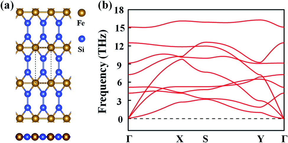 | ||
| Fig. 1 (a) Top and side views of the FeSi2 monolayer. The dashed lines represent a unit cell, while a, b and c represent the lattice vectors. (b) Phonon spectrum of the FeSi2 monolayer. | ||
The dynamic stability of the FeSi2 monolayer was confirmed by the phonon spectrum. As seen in Fig. 1(b), there is no imaginary frequency in the entire Brillouin zone, indicating that the configuration is stable against distortion perturbation. Furthermore, the evolution of total energy and snapshots of the final structures of the FeSi2 monolayer at different temperatures from AIMD simulations are shown in Fig. S1.† The framework of the FeSi2 monolayer is well maintained at 600 K, with the energy fluctuating in a small range (∼0.12 eV per atom). These results confirm that the FeSi2 monolayer has good thermal stability and could be used in devices under high-temperature conditions.
In addition, we calculated the 2D elastic constants of the FeSi2 monolayer, which are C11 = 85.72 N m−1, C22 = 154.10 N m−1, C66 = 34.26 N m−1, and C12 = C21 = 32.02 N m−1. According to the Born criteria, the mechanical stability of the FeSi2 monolayer, which belongs to the orthorhombic system, should satisfy C66 > 0 and C11C22 − 2C122 > 0.43 Clearly, both criteria are well satisfied, indicating that the FeSi2 monolayer structure is mechanically stable.
To better describe the type of chemical bonding in the FeSi2 monolayer, SSAdNDP analyses were performed for a 3 × 1 × 1 supercell by considering spin polarization, and the results for two spin channels are shown in Fig. 2. For the spin-up states, there are twelve single electrons, three two-center-one-electron (2c–1e) σ bonds, six 3c–1e σ bonds, three 4c–1e σ bonds, and three 7c–1e π bonds. For the spin-down states, there are six single electrons occupying Fe atoms, three 2c–1e σ bonds, six 3c–1e σ bonds, three 4c–1e σ bonds, and three 7c–1e π bonds. These results unveil that the existence of multi-center delocalized bonds and abundant π bonds is helpful to maintain the planar stability of the FeSi2 monolayer.
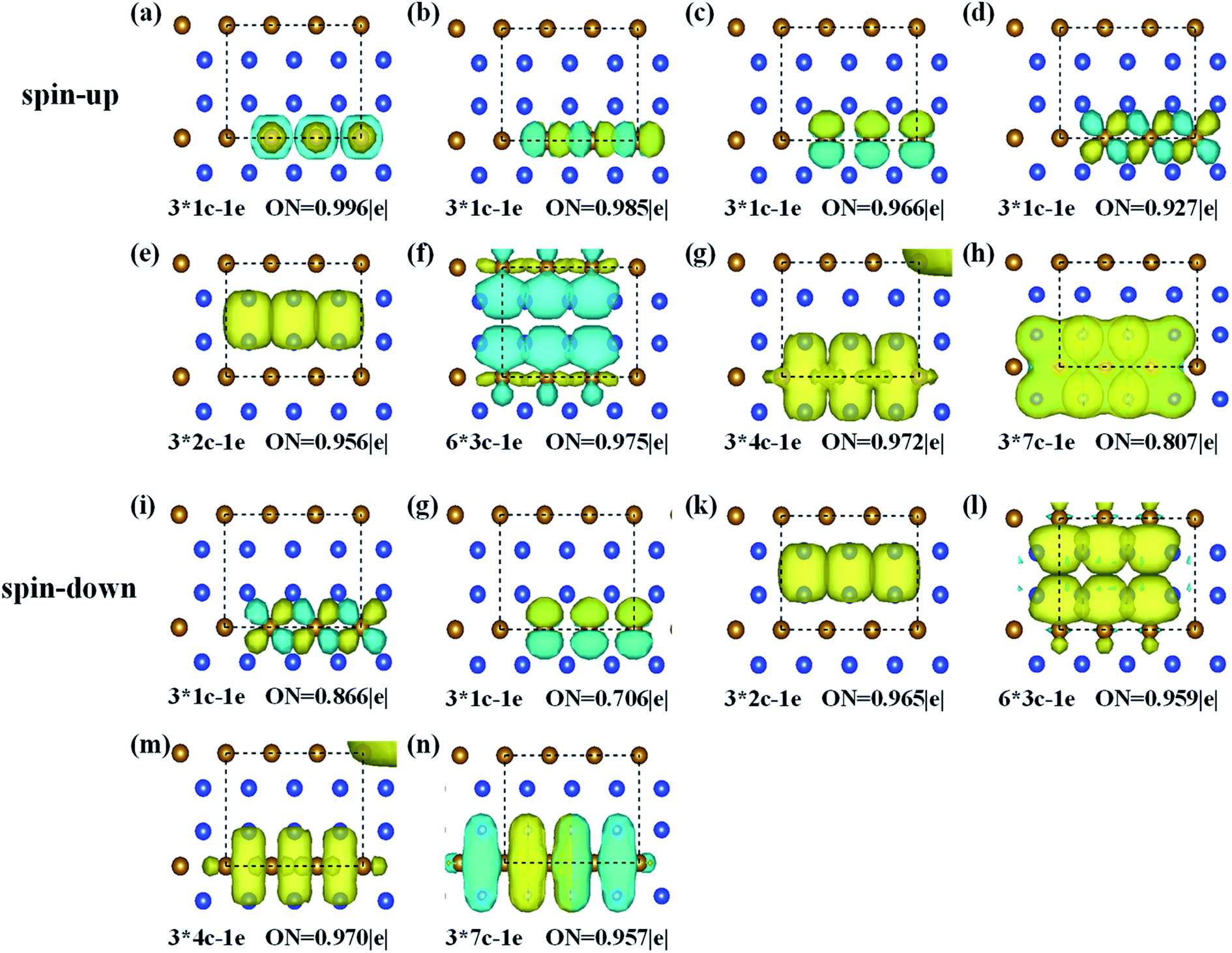 | ||
| Fig. 2 SSAdNDP chemical bonding patterns of the FeSi2 monolayer. ON denotes the occupation number. The yellow and cyan represent positive and negative charge regions, respectively. The results for the spin-up and spin-down states are presented separately. | ||
To further understand the bonding nature of the FeSi2 monolayer, we calculated the electron localization function (ELF). As shown in Fig. S2(a),† the ELF isosurface shows substantial accumulation of electrons in the middle of Si–Si bonds, indicating strong covalent interactions in the Si network. In contrast, the Fe atoms are electron deficient with a nearly zero ELF value. Differential charge density and Hirshfeld charge analyses were also performed to reveal the charge transfer behavior between Fe and Si atoms.44 The differential charge density in Fig. S2(b)† shows that charge transfer occurs from Fe atoms to Si atoms; the charge density is delocalized over the Fe–Si bonds, contributing to the stabilization of the FeSi2 monolayer. Hirshfeld charge analysis reveals that each Fe atom donates about 0.084 electrons to the adjacent Si atoms. The charge accumulation on Fe–Si bonds and the small amount of charge transfer between Fe atoms and Si atoms indicate covalent interactions between these two types of atoms. As in the cases of Cu2Si (∼0.06|e|) and FeB2 (∼0.051|e|) monolayer structures, such a small amount of charge transfer is sufficient to ensure the stability of 2D lattices.8,10
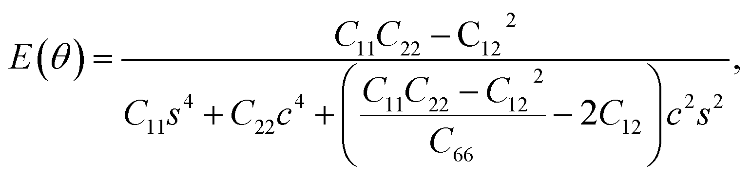
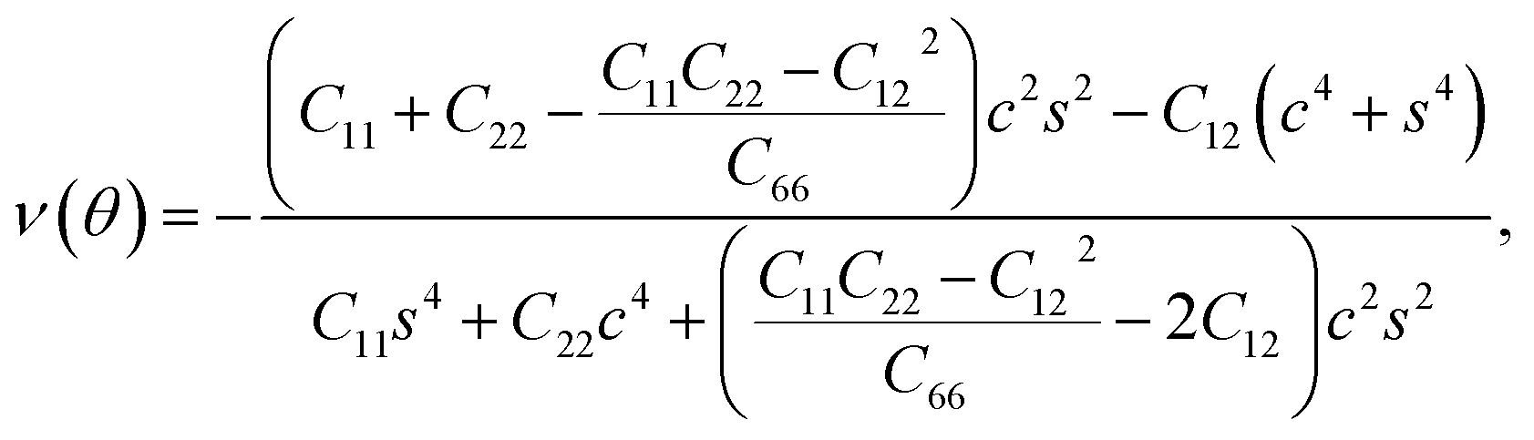
Furthermore, we examined the in-plane Young's modulus E(θ) and Poisson ratio ν(θ) along any direction θ (where θ is the angle relative to the positive a direction), which can be calculated as follows:45
 | (3) |
 | (4) |
![[thin space (1/6-em)]](https://www.rsc.org/images/entities/char_2009.gif) θ, and s = sinθ. The calculated E(θ) and ν(θ) values in Fig. S3† indicate that the Young's modulus in the b direction has a maximum value of 142 N m−1, which is approximately two times larger than that in the a direction. This value is smaller than that of graphene (341 N m−1), but larger than that of the Cu2Si monolayer (93 N m−1) and the MoS2 monolayer (129 N m−1).7,46,47 The Poisson ratio is also anisotropic with a maximum value of 0.37 along the a direction and a minimum value of 0.21 along the b direction. The prominent anisotropy in both the Young's modulus and Poisson ratio implies that the FeSi2 monolayer may have intriguing mechanical applications.
θ, and s = sinθ. The calculated E(θ) and ν(θ) values in Fig. S3† indicate that the Young's modulus in the b direction has a maximum value of 142 N m−1, which is approximately two times larger than that in the a direction. This value is smaller than that of graphene (341 N m−1), but larger than that of the Cu2Si monolayer (93 N m−1) and the MoS2 monolayer (129 N m−1).7,46,47 The Poisson ratio is also anisotropic with a maximum value of 0.37 along the a direction and a minimum value of 0.21 along the b direction. The prominent anisotropy in both the Young's modulus and Poisson ratio implies that the FeSi2 monolayer may have intriguing mechanical applications.
Next, we discuss the electronic properties of the FeSi2 monolayer. The spin-polarized band structures are displayed in Fig. 3(a). Several bands in both spin-up and spin-down channels cross the Fermi level; thus, the FeSi2 monolayer is metallic. We also employ the Heyd–Scouseria–Ernzerhof (HSE06) functional to further confirm its band characteristics. As shown in Fig. S4,† the FeSi2 monolayer still exhibits a metallic nature. As revealed by the partial density of states (PDOS) of the FeSi2 monolayer in Fig. 3(b), the density of states at the Fermi level is mainly contributed by Fe 3d orbitals.
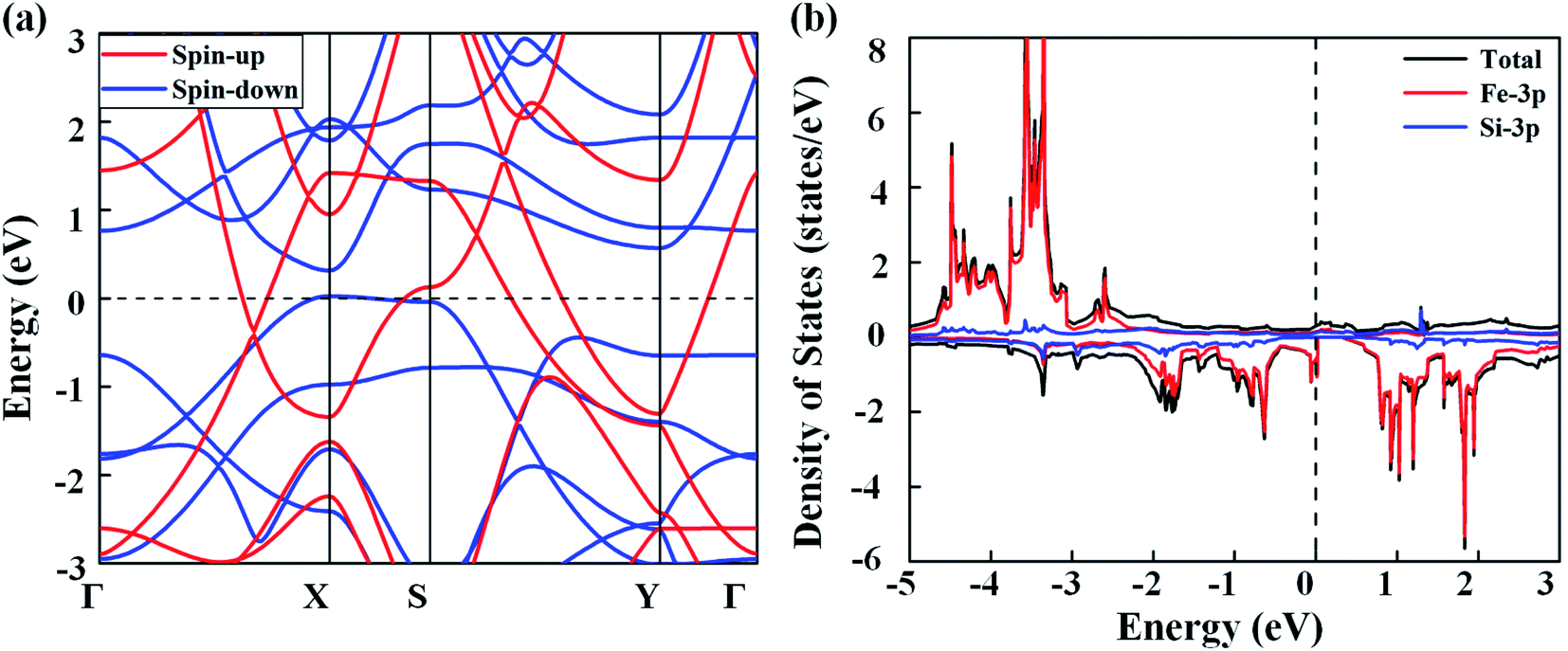 | ||
| Fig. 3 (a) Spin-polarized band structures of the FeSi2 monolayer. (b) Total and partial density of states of the FeSi2 monolayer. The Fermi level (dashed line) is set to zero. | ||
The calculated spin polarization of electrons in Fig. 4(a) indicates that the magnetism mainly originates from Fe with a magnetic moment of 2.27 μB per Fe atom, which can be explained within the framework of crystal field theory [see Fig. 4(b)]. Due to symmetry breaking under the planar hexagonal crystal field, the five degenerate d orbitals of the Fe atom split into three groups: the degenerate dxy and dx2−y2 orbitals with higher energy, the dz2 orbital with intermediate energy, and the degenerate dyz and dxz orbitals with lower energy. In the FeSi2 monolayer, distortion of the hexagonal plane leads to further splitting of the orbitals so that the five d orbitals are no longer degenerate. According to the above bonding analysis, although there is a small amount of charge transfer between the Fe and Si atoms, the total number of valence electrons on the Fe atom ([Ar]3d74s1) remains nearly intact. Because of the competition between the Coulomb repulsion and the crystal field splitting energy, electrons will first occupy the orbitals with parallel spin according to Hund's rule. Finally, all five spin-up d orbitals are occupied, while the spin-down dxz and dz2 orbitals are left empty. Hence, the spin magnetic moment on each Fe atom should be approximately 2.0 μB, consistent with the PDOS picture for the Fe atom from DFT calculations [Fig. 4(c)]. The above SSAdNDP analysis shows that in the 3 × 1 × 1 supercell, the spin-up states of six 1c–1e bonds on Fe atoms are unpaired, resulting in the spin polarization of the system. In the supercell, the difference between the numbers of occupied spin-up and spin-down states from the SSAdNDP analysis is about 6.53|e|, which is almost the same as the calculated magnetic moment of ∼6.34 μB.
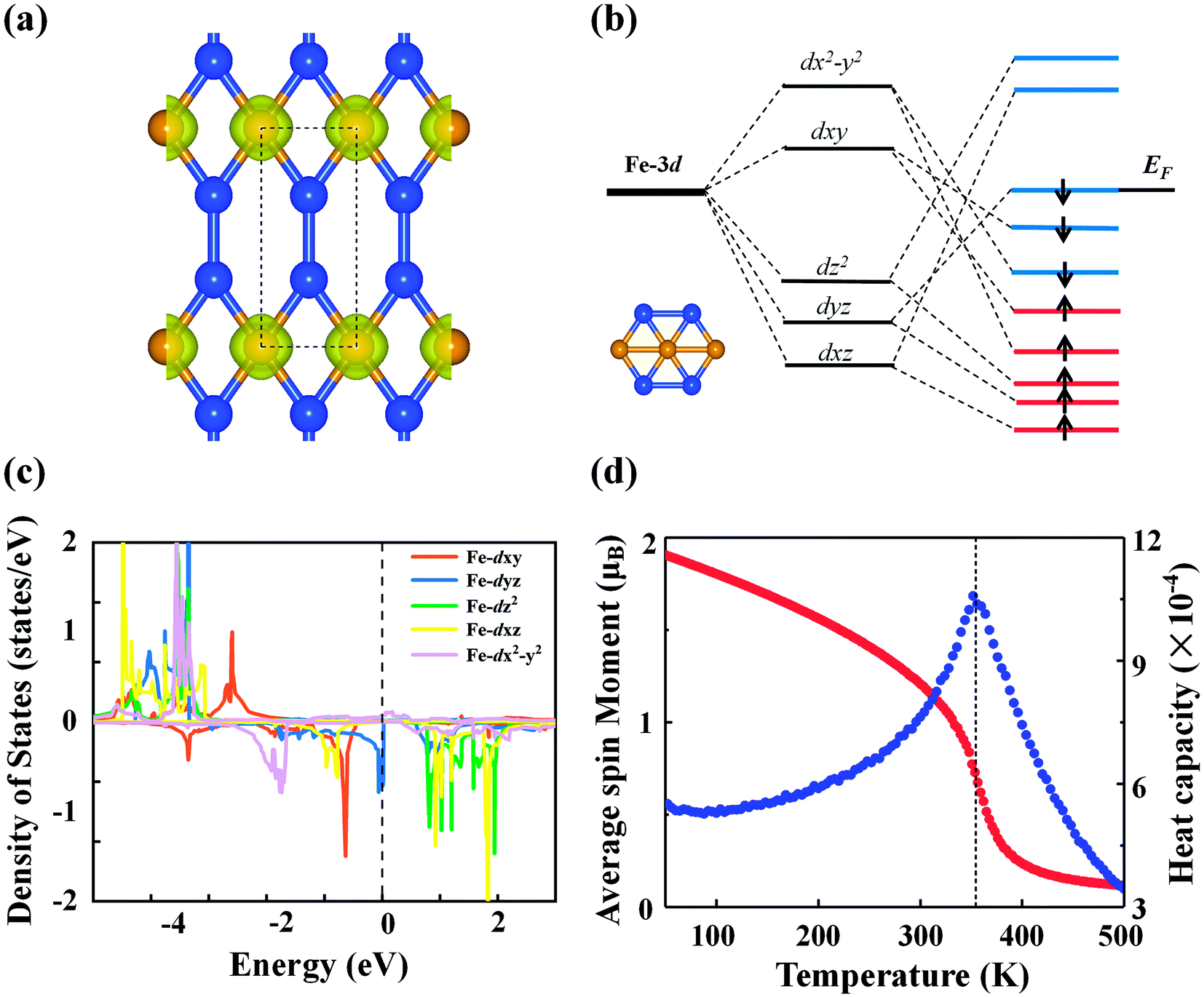 | ||
| Fig. 4 (a) Spin density distributions of the FeSi2 monolayer with an isosurface of 0.015 au. The dashed lines represent a unit cell. (b) Splitting of the d orbitals of the Fe atom in the crystal field. The inset is a schematic structure of the distorted hexagonal plane in the FeSi2 monolayer. (c) Partial orbital density of states of the Fe atom in the FeSi2 monolayer. (d) Average magnetic moment per Fe atom (red scatter) and heat capacity (blue scatter) of the FeSi2 monolayer as a function of temperature from Monte Carlo simulations. | ||
The magnetic ground state of the FeSi2 monolayer was determined by comparing the energy of the FM state with those of seven AFM configurations shown in Fig. S5.† The energy differences of different AFM configurations relative to the FM state are listed in Table S1,† demonstrating that the ground state is FM. Also note that the magnetic moment and magnetic ground state are not affected by the HSE06 functional. In order to understand the magnetic exchange mechanism in the FeSi2 monolayer, we considered seven-order spin-exchange interaction (Fig. S5†) to ensure that the exchange parameter Ji can converge to a small value. The exchange parameter Ji and the corresponding Fe–Fe distance di are listed in Table S2.† As the distance between the magnetic atoms increases, the exchange parameter Ji does not decrease consistently; instead, Ji oscillates with an overall decreasing trend. This suggests that the magnetic exchange mechanism in the FeSi2 monolayer belongs to the indirect Ruderman–Kittel–Kasuya–Yosida (RKKY) interaction, similar to that of the planar hypercoordinate FeB3 monolayer reported before.16 Using the exchange parameter Ji, we performed Monte Carlo (MC) simulation based on the 2D Heisenberg model to estimate the Curie temperature of the FeSi2 monolayer. The Curie temperature [Fig. 4(d)] is approximately 360 K, which is above room temperature and higher than those of 2D planar FM monolayers of χ3 CrB4 (242 K) and orthorhombic phase FeC2 (245 K), both belonging to 2D hypercoordinate compounds by transition metals and light nonmetal elements.48,49 Taking spin–orbit coupling into account, we further compared the energies of the FeSi2 monolayer among four magnetization directions, namely, (100), (010), (110), and (001). The easy magnetization axis is along the (100) direction with a MAE of 56 μeV per Fe atom.
With all these unique chemical and physical properties, we expect to prepare this FeSi2 monolayer experimentally. Since its 3D FeSi2 parent is a non-vdW layered material, it is difficult to obtain a FeSi2 monolayer by mechanical exfoliation. However, such a 2D non-vdW material may synthesize directly on a suitable substrate by the molecular beam epitaxy (MBE) or chemical vapor deposition (CVD) method. Based on the two methods, several 2D non-vdW ultrathin films have been recently synthesized successfully.50,51 Among the low-index Si surfaces, the Si (110) surface has been widely used in the synthesis of electronic devices, and the Si (110) surface also has higher hole mobility than the other surfaces.52–54 Upon using our structural model of the (2 × 3) FeSi2 monolayer on the (1 × 5) Si (110) surface, the lattice mismatch is less than 3% upon relaxation. In order to accommodate the strain energy caused by lattice mismatch, the Fe–Si bond length in the heterostructure changes and the Si-supported FeSi2 layer is slightly distorted compared to the freestanding monolayer [Fig. 5(a)]. The interlayer distance between the FeSi2 monolayer and Si (110) surface is about 2.28 Å. Specifically, the average distance between Fe atoms and substrate Si atoms is about 2.64 Å, which is comparable to the covalent Fe–Si bond length (2.40 Å) in the freestanding FeSi2 monolayer.
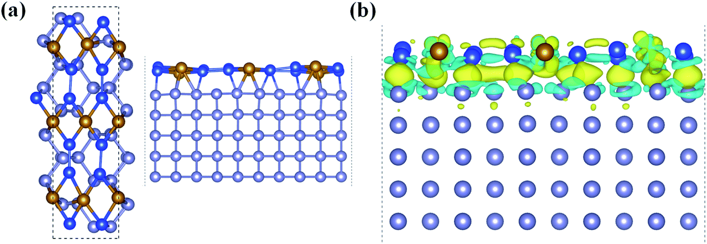 | ||
| Fig. 5 (a) Top and side views of the FeSi2 monolayer on the Si (110) substrate. (b) Differential charge density between the FeSi2 monolayer and the Si (110) surface, with an isosurface value of 4 × 10⁻³ e × Å−3. The yellow and cyan regions represent electron accumulation and depletion, respectively. | ||
To describe the interfacial interaction between the FeSi2 monolayer and Si (110) substrate, we calculated the formation energy defined as:
| Ef = (Etot − EFeSi2 − Esub)/Natom, | (5) |
In addition, we plotted the differential charge density to visually show the interface interaction between the monolayer and substrate, as shown in Fig. 5(b). Obviously, due to the strong interface interaction between the FeSi2 monolayer and Si (110) surface, the charge is redistributed near the interface, which is conducive to interface adhesion, suggesting that the FeSi2 monolayer can be grown directly on the Si (110) substrate. The method of preparing a 2D thin film by using the strong interaction between the film and substrate has been widely used in experiments.57–61 For future experimental identification, we also simulated the STM image of the FeSi2 monolayer on the Si (110) surface. The bright areas in the simulated STM image are associated with Fe atoms (see the labels in Fig. S6†).
We also examined the effects of the substrate on the electronic and magnetic properties of the FeSi2 monolayer. As shown in Fig. S7,† compared with the freestanding FeSi2 monolayer without the Si (110) substrate, the DOS peak of the freestanding FeSi2 monolayer with the substrate becomes flatter and the peak decreases, which may be due to the formation of chemical bonds by charge transfer between the FeSi2 monolayer and substrate. The energy differences between the FM and AFM states (Table S2†) indicate that the magnetic ground state of the FeSi2 monolayer on the silicon substrate remains in the FM state. In comparison to the case of the freestanding monolayer, the MAE and average magnetic moment of the FeSi2 monolayer on the silicon substrate are enhanced to 1.34 meV per Fe atom and 2.87 μB per Fe atom, respectively, and the easy magnetization axis remains in the in-plane direction. These findings indicate that the Si (110) substrate not only provides a structural template for the deposited FeSi2 film but the interaction between the film and the substrate itself leads to enhanced magnetic properties.
4. Conclusions
In summary, we designed a new stable planar hexacoordinate 2D FeSi2 monolayer in which each Fe atom is coordinated to four Si atoms and two adjacent Fe atoms. Based on first-principles calculations, we comprehensively explored the mechanical, electronic, and magnetic properties of the FeSi2 monolayer. The results revealed that the monolayer has in-plane mechanical anisotropy and high stability due to abundant multicenter bonds. Notably, the FeSi2 monolayer exhibits strong intrinsic ferromagnetism with a high TC (∼360 K). The robust magnetic coupling can be attributed to the indirect RKKY interaction. Furthermore, we predicted that the FeSi2 monolayer can grow directly on the insulating Si (110) substrate, meanwhile the magnetic moment and MAE can be significantly improved. Our findings enrich the diversity of planar hypercoordinate transition metal compounds, and the attractive properties revealed in this study make the FeSi2 monolayer a promising candidate for applications in spintronics.Conflicts of interest
There are no conflicts to declare.Acknowledgements
This work was supported by the Genetic Engineering of Precious Metal Materials in Yunnan Province (I)-Construction and Application of Precious Metal Materials Professional Database (I) (202002AB080001-1), Science Challenge Project (TZ2018004) and National Natural Science Foundation of China (11874097). We acknowledge the Xinghai Scholar project of Dalian University of Technology. The authors also acknowledge the Supercomputing Center of Dalian University of Technology for providing the computing resources.References
- R. Hoffmann, R. W. Alder and C. F. Wilcox Jr, J. Am. Chem. Soc., 1970, 92, 4992–4993 CrossRef CAS.
- J. A. Le Bel, Bull. Soc. Chim. Fr., 1874, 22, 337–347 Search PubMed.
- Y. Wang, Y. Li and Z. Chen, Acc. Chem. Res., 2020, 53, 887–895 CrossRef CAS PubMed.
- C.-S. Liu, H.-H. Zhu, X.-J. Ye and X.-H. Yan, Nanoscale, 2017, 9, 5854–5858 RSC.
- X. Qu, J. Yang, Y. Wang, J. Lv, Z. Chen and Y. Ma, Nanoscale, 2017, 9, 17983–17990 RSC.
- H. Zhang, Y. Li, J. Hou, K. Tu and Z. Chen, J. Am. Chem. Soc., 2016, 138, 5644–5651 CrossRef CAS PubMed.
- B. Feng, B. Fu, S. Kasamatsu, S. Ito, P. Cheng, C.-C. Liu, Y. Feng, S. Wu, S. K. Mahatha, P. Sheverdyaeva, P. Moras, M. Arita, O. Sugino, T.-C. Chiang, K. Shimada, K. Miyamoto, T. Okuda, K. Wu, L. Chen, Y. Yao and I. Matsuda, Nat. Commun., 2017, 8, 1007 CrossRef PubMed.
- H. Zhang, Y. Li, J. Hou, A. Du and Z. Chen, Nano Lett., 2016, 16, 6124–6129 CrossRef CAS PubMed.
- Y. Wang, M. Qiao, Y. Li and Z. Chen, Nanoscale Horiz., 2018, 3, 327–334 RSC.
- L.-M. Yang, V. Bačić, I. A. Popov, A. I. Boldyrev, T. Heine, T. Frauenheim and E. Ganz, J. Am. Chem. Soc., 2015, 137, 2757–2762 CrossRef CAS PubMed.
- L.-M. Yang, M. Dornfeld, T. Frauenheim and E. Ganz, Phys. Chem. Chem. Phys., 2015, 17, 26036–26042 RSC.
- L.-M. Yang, T. Frauenheim and E. Ganz, J. Nanomater., 2016, 2016 Search PubMed.
- L.-M. Yang and E. Ganz, Phys. Chem. Chem. Phys., 2016, 18, 17586–17591 RSC.
- L.-M. Yang, I. A. Popov, A. I. Boldyrev, T. Heine, T. Frauenheim and E. Ganz, Phys. Chem. Chem. Phys., 2015, 17, 17545–17551 RSC.
- C. Zhu, H. Lv, X. Qu, M. Zhang, J. Wang, S. Wen, Q. Li, Y. Geng, Z. Su, X. Wu, Y. Li and Y. Ma, J. Mater. Chem. C, 2019, 7, 6406–6413 RSC.
- C. Tang, K. Ostrikov, S. Sanvito and A. Du, Nanoscale Horiz., 2021, 6, 43–48 RSC.
- K. S. Novoselov, A. K. Geim, S. V. Morozov, D. Jiang, Y. Zhang, S. V. Dubonos, I. V. Grigorieva and A. A. Firsov, Science, 2004, 306, 666–669 CrossRef CAS PubMed.
- M. P. Warusawithana, C. Cen, C. R. Sleasman, J. C. Woicik, Y. L. Li, L. F. Kourkoutis, J. A. Klug, H. Li, P. Ryan, L. P. Wang, M. Bedzyk, D. A. Muller, L. Q. Chen, J. Levy and D. G. Schlom, Science, 2009, 324, 367–370 CrossRef CAS PubMed.
- J. Jeon, S. K. Jang, S. M. Jeon, G. Yoo, Y. H. Jang, J.-H. Park and S. Lee, Nanoscale, 2015, 7, 1688–1695 RSC.
- N. Mounet, M. Gibertini, P. Schwaller, D. Campi, A. Merkys, A. Marrazzo, T. Sohier, I. E. Castelli, A. Cepellotti, G. Pizzi and N. Marzari, Nat. Nanotechnol., 2018, 13, 246–252 CrossRef CAS PubMed.
- W. Heywang and K. H. Zaininger, in Silicon, Springer, 2004, pp. 25–42 Search PubMed.
- T. Mårtensson, C. P. T. Svensson, B. A. Wacaser, M. W. Larsson, W. Seifert, K. Deppert, A. Gustafsson, L. R. Wallenberg and L. Samuelson, Nano Lett., 2004, 4, 1987–1990 CrossRef.
- G. Kresse and J. Hafner, Phys. Rev. B: Condens. Matter Mater. Phys., 1993, 47, 558–561 CrossRef CAS PubMed.
- J. Hafner, J. Comput. Chem., 2008, 29, 2044–2078 CrossRef CAS PubMed.
- P. E. Blöchl, Phys. Rev. B: Condens. Matter Mater. Phys., 1994, 50, 17953 CrossRef PubMed.
- G. Kresse and D. Joubert, Phys. Rev. B, 1999, 59, 1758–1775 CrossRef CAS.
- J. P. Perdew, K. Burke and M. Ernzerhof, Phys. Rev. Lett., 1996, 77, 3865–3868 CrossRef CAS PubMed.
- H. J. Monkhorst and J. D. Pack, Phys. Rev. B: Solid State, 1976, 13, 5188–5192 CrossRef.
- S. Iv, P. H. Dederichs and A. Vi, Phys. Rev. B: Condens. Matter Mater. Phys., 1994, 50, 16861–16871 CrossRef PubMed.
- A. Togo, F. Oba and I. Tanaka, Phys. Rev. B: Condens. Matter Mater. Phys., 2008, 78, 134106 CrossRef.
- M. Lan, G. Xiang, Y. Nie, D. Yang and X. Zhang, RSC Adv., 2016, 6, 31758–31761 RSC.
- M. Kan, J. Zhou, Q. Sun, Y. Kawazoe and P. Jena, J. Phys. Chem. Lett., 2013, 4, 3382–3386 CrossRef CAS PubMed.
- L. Liu, S. Chen, Z. Lin and X. Zhang, J. Phys. Chem. Lett., 2020, 11, 7893–7900 CrossRef CAS PubMed.
- T. R. Galeev, B. D. Dunnington, J. R. Schmidt and A. I. Boldyrev, Phys. Chem. Chem. Phys., 2013, 15, 5022–5029 RSC.
- E. D. Glendening, C. R. Landis and F. Weinhold, Wiley Interdiscip. Rev.: Comput. Mol. Sci., 2012, 2, 1–42 CAS.
- D. Y. Zubarev and A. I. Boldyrev, Phys. Chem. Chem. Phys., 2008, 10, 5207–5217 RSC.
- S. Grimme, S. Ehrlich and L. Goerigk, J. Comput. Chem., 2011, 32, 1456–1465 CrossRef CAS PubMed.
- G. Henkelman, A. Arnaldsson and H. Jónsson, Comput. Mater. Sci., 2006, 36, 354–360 CrossRef.
- J. Tersoff and D. R. Hamann, Phys. Rev. Lett., 1983, 50, 1998–2001 CrossRef CAS.
- J. Tersoff and D. R. Hamann, Phys. Rev. B: Condens. Matter Mater. Phys., 1985, 31, 805–813 CrossRef CAS PubMed.
- K. Palotas and W. A. Hofer, J. Phys.: Condens. Matter, 2005, 17, 2705–2713 CrossRef CAS.
- C. Kloc, E. Arushanov, M. Wendl, H. Hohl, U. Malang and E. Bucher, J. Alloys Compd., 1995, 219, 93–96 CrossRef CAS.
- J. Wang, S. Yip, S. R. Phillpot and D. Wolf, Phys. Rev. Lett., 1993, 71, 4182–4185 CrossRef CAS PubMed.
- P. Bultinck, C. Van Alsenoy, P. W. Ayers and R. Carbó-Dorca, J. Phys. Chem. C, 2007, 126, 144111 CrossRef PubMed.
- E. Cadelano, P. L. Palla, S. Giordano and L. Colombo, Phys. Rev. B: Condens. Matter Mater. Phys., 2010, 82, 235414 CrossRef.
- R. C. Cooper, C. Lee, C. A. Marianetti, X. Wei, J. Hone and J. W. Kysar, Phys. Rev. B: Condens. Matter Mater. Phys., 2013, 87, 035423 CrossRef.
- C. Lee, X. Wei, J. W. Kysar and J. Hone, Science, 2008, 321, 385 CrossRef CAS PubMed.
- X. Li, X. Li and J. Yang, J. Phys. Chem. Lett., 2019, 10, 4417–4421 CrossRef CAS PubMed.
- T. Zhao, J. Zhou, Q. Wang, Y. Kawazoe and P. Jena, ACS Appl. Mater. Interfaces, 2016, 8, 26207–26212 CrossRef CAS PubMed.
- L. Kang, C. Ye, X. Zhao, X. Zhou, J. Hu, Q. Li, D. Liu, C. M. Das, J. Yang and D. Hu, Nat. Commun., 2020, 11, 1–9 Search PubMed.
- A. Roy, S. Guchhait, R. Dey, T. Pramanik, C.-C. Hsieh, A. Rai and S. K. Banerjee, ACS Nano, 2015, 9, 3772–3779 CrossRef CAS PubMed.
- W. Cheng, A. Teramoto, M. Hirayama, S. Sugawa and T. Ohmi, Jpn. J. Appl. Phys., 2006, 45, 3110 CrossRef CAS.
- F. Ruiz-Zepeda, O. Contreras, A. Dadgar and A. Krost, Appl. Phys. Lett., 2010, 96, 231908 CrossRef.
- T. Satô, Y. Takeishi, H. Hara and Y. Okamoto, Phys. Rev. B: Solid State, 1971, 4, 1950–1960 CrossRef.
- N. Gao, H. Liu, S. Zhou, Y. Bai and J. Zhao, J. Phys. Chem. C, 2017, 121, 5123–5129 CrossRef CAS.
- X. Tan, F. Li and Z. Chen, J. Phys. Chem. C, 2014, 118, 25825–25835 CrossRef CAS.
- W. Chang, S. Rajan, B. Peng, C. Ren, M. Sutton and C. Li, Carbon, 2019, 153, 699–706 CrossRef CAS.
- L. Ding, W. Zhou, T. P. McNicholas, J. Wang, H. Chu, Y. Li and J. Liu, Nano Res., 2009, 2, 903–910 CrossRef CAS.
- M. Velicky, A. Rodriguez, M. Bousa, A. V. Krayev, M. Vondracek, J. Honolka, M. Ahmadi, G. E. Donnelly, F. Huang, H. D. Abruna, K. S. Novoselov and O. Frank, J. Phys. Chem. Lett., 2020, 11, 6112–6118 CrossRef CAS PubMed.
- S. Wang, X. Wang and J. H. Warner, ACS Nano, 2015, 9, 5246–5254 CrossRef CAS PubMed.
- X. H. Ye, F. Yu, M. Curioni, Z. Lin, H. J. Zhang, H. W. Zhu, Z. Liu and M. L. Zhong, RSC Adv., 2015, 5, 35384–35390 RSC.
Footnote |
| † Electronic supplementary information (ESI) available. See DOI: 10.1039/d1na00772f |
| This journal is © The Royal Society of Chemistry 2022 |