
 Open Access Article
 This Open Access Article is licensed under a Creative Commons Attribution-Non Commercial 3.0 Unported Licence
Colloidal 2D PbSe nanoplatelets with efficient emission reaching the telecom O-, E- and S-band†
Lars F.
Klepzig
 ab,
Leon
Biesterfeld
ab,
Michel
Romain
a,
André
Niebur
ab,
Anja
Schlosser
ac,
Jens
Hübner
cd and
Jannika
Lauth
*abc
ab,
Leon
Biesterfeld
ab,
Michel
Romain
a,
André
Niebur
ab,
Anja
Schlosser
ac,
Jens
Hübner
cd and
Jannika
Lauth
*abc
aInstitute of Physical Chemistry and Electrochemistry, Leibniz Universität Hannover, Callinstr. 3A, 30167 Hannover, Germany. E-mail: jannika.lauth@pci.uni-hannover.de
bCluster of Excellence PhoenixD (Photonics, Optics, and Engineering – Innovation Across Disciplines), 30167 Hannover, Germany
cLaboratory of Nano and Quantum Engineering (LNQE), Leibniz Universität Hannover, Schneiderberg 39, 30167 Hannover, Germany
dInstitute of Solid State Physics, Leibniz Universität Hannover, Appelstraße 2, 30167 Hannover, Germany
First published on 15th December 2021
Abstract
Colloidal two-dimensional (2D) lead chalcogenide nanoplatelets (NPLs) represent highly interesting materials for near- and short wave-infrared applications including innovative glass fiber optics exhibiting negligible attenuation. In this work, we demonstrate a direct synthesis route for 2D PbSe NPLs with cubic rock salt crystal structure at low reaction temperatures of 0 °C and room temperature. A lateral size tuning of the PbSe NPLs by controlling the temperature and by adding small amounts of octylamine to the reaction leads to excitonic absorption features in the range of 1.55–1.24 eV (800–1000 nm) and narrow photoluminescence (PL) reaching the telecom O-, E- and S-band (1.38–0.86 eV, 900–1450 nm). The PL quantum yield of the as-synthesized PbSe NPLs is more than doubled by a postsynthetic treatment with CdCl2 (e.g. from 14.7% to 37.4% for NPLs emitting at 980 nm with a FWHM of 214 meV). An analysis of the slightly asymmetric PL line shape of the PbSe NPLs and their characterization by ultrafast transient absorption and time-resolved PL spectroscopy reveal a surface trap related PL contribution which is successfully reduced by the CdCl2 treatment from 40% down to 15%. Our results open up new pathways for a direct synthesis and straightforward incorporation of colloidal PbSe NPLs as efficient infrared emitters at technologically relevant telecom wavelengths.
Introduction
Atomically-thin quasi-two-dimensional (2D) IV–VI semiconductors, especially lead chalcogenide nanosheets (NSs) and nanoplatelets (NPLs), have attracted significant interest due to their promising optoelectronic properties covering the near-infrared (NIR) and short-wave-infrared (SWIR) wavelength range of the electromagnetic spectrum.1–3 2D NSs and NPLs belong to the same category with NPLs typically showing lateral sizes <100 nm. The materials exhibit broadly tunable absorption and photoluminescence (PL) properties, which are controlled mainly by their quantum-confined thickness and provide access to the spectral windows needed in biological imaging or fiber optics.4–6 2D lead chalcogenide NSs for example show photophysics different from their spherical nanocrystal (NC) counterparts such as strong Rashba spin–orbit coupling,7 even more efficient carrier multiplication,8 and high charge carrier mobility.9,10 This allows for their use as active optical components for field effect transistors (FETs),11 light-emitting diodes (LEDs),12 or solar cells.13,14 Additionally, colloidal lead chalcogenides are highly interesting nanomaterials for deterministic single photon emission which is applied in photonic quantum technologies like quantum key distribution.15–18However, synthetic access, especially to NPLs exhibiting seamlessly tunable and efficient NIR to SWIR PL is scarce. For example, Tenney et al. synthesized HgTe NPLs decorated with HgTe NCs that exhibited efficient PL with a quantum yield (QY) of >30% between 1000 and 1500 nm. The synthesis is elaborate, requiring a cation exchange from CdSe NPLs and a simultaneous ligand exchange.19 A similar cation exchange approach from CdSe NPLs to PbSe NPLs has been described by Galle et al.20,21 The starting CdSe NPLs show high brightness and narrow PL that is partly retained during the cation exchange.22 Thin cation exchanged PbSe NPLs from 4 monolayer (ML) CdSe yielded a PLQY of 15% centered at 1330 nm, whereas the thickest PbSe NPLs of 6 ML exhibited a PLQY of 6% centered at 1545 nm.20
While straightforward and direct colloidal synthesis methods for PbS and PbSe NCs are well established, relatively few studies deal with the direct synthesis of strongly confined IV–VI semiconductor NPLs,2,23–28 even less based on PbSe.3 Recently, we have shown the synthesis of ultrathin PbS NPLs with enhanced NIR emission.29
The synthesis of cubic 2D NSs and NPLs requires anisotropic crystal growth, which can be induced by different strategies including oriented attachment leading to symmetry breaking,1,3,30 cation exchange,20,31 templated growth,26,32,33 and intrinsic instabilities leading to enhanced growth of the basal plane.34
Koh et al. describe the synthesis of thickness-controlled 2D PbSe NPLs by oriented attachment of PbSe NCs.3 They find a crucial role of halide ions to be responsible for a 2D bridging of the NCs, whereas the thickness is controlled by the amount of PbI2 added. While a tunable PL was achieved by controlling the NPL thickness, the measured PLQY of ∼0.1% was rather low.
Here, we report the first direct synthesis of 2D PbSe NPLs with efficient broadband tunable infrared emission by using lead oleate and selenourea as precursors in a mixture of octylamine and oleic acid.35–37 PbSe NPLs are synthesized at room temperature or below and exhibit distinct excitonic absorption features between 800–1000 nm (1.55–1.24 eV), while narrow PL is obtained at technologically relevant telecommunication wavelengths between 900–1450 nm (1.38–0.86) eV, reaching the O-, E- and S-band (0.98–0.91, 0.91–0.85 and 0.85–0.81 eV, resp.). By adjusting the reaction temperature and the amount of octylamine used for the synthesis, the optical properties of the NPLs are tuned by controlling their lateral size rather than their thickness. In a subsequent step, a postsynthetic surface treatment of the PbSe NPLs with CdCl2 leads to a general doubling of the PLQY of PbSe NPLs (e.g., from 14.7% to 37.4% for NPLs emitting at 980 nm), exceeding the best results for PbSe NPLs published so far.
Experimental
Chemicals
Octylamine (OcAm, 99.0%), oleic acid (HOA, ≥99%) and cadmium chloride (CdCl2, 99.99%) were purchased from Sigma-Aldrich/Merck. Selenourea (99.97%) and analytical grade hexane (99.99%, anhydrous) were purchased from Alfa Aesar. Ethanol (99.9%, extra dry) was purchased from Acros. Tetrachloroethylene (TCE, ≥99.9%, anhydrous) was purchased from Merck-Millipore. Octylamine was dried via freeze–pump–thawing for three times. All other reagents were used as received without further purification.Synthesis of the lead oleate precursor (Pb(OA)2)
The synthesis of lead oleate is based on a method described by Hendricks et al. and has been recently proven successful for the synthesis of 2D PbS NPLs.31,38 Briefly, 5 g (22.4 mmol) lead oxide were stirred in 10 mL acetonitrile for 10 min at 0 °C. The solution turned clear after the addition of 0.35 mL (4.54 mmol) trifluoroacetic acid and 3.1 mL (22.3 mmol) trifluoroacetic anhydride and was allowed to reach room temperature. A separate solution of 14.2 mL (45.0 mmol) HOA, 7.1 mL (50.6 mmol) triethylamine and 90 mL isopropanol was prepared and added to the lead solution. The white precipitate was purified by recrystallization after refluxing at 80 °C for 10 min until a clear solution was obtained. The solution was stored in a freezer (−20 °C) for 19 h before being filtered and washed with methanol. The dried lead oleate was stored in a glovebox at −24 °C.Synthesis of the selenourea precursor
In a 9 mL vial, a mixture of 193 mg (1.57 mmol) selenourea, 2 mL (12 mmol) OcAm, 0.2 mL (0.7 mmol) HOA and 0.75 mL hexane was prepared. The mixture was stirred at 35 °C at least for 24 h until a clear dark-orange solution was obtained. The selenium precursor was used for up to five days.PbSe NPL synthesis
The synthesis of PbSe NPLs is based on a method by Manteiga Vázquez et al.29 The precursor formation steps and the reaction were run under inert gas conditions either inside a glovebox or on a Schlenk apparatus. The syntheses at 0 °C were conducted using an ice bath. In a 9 mL vial, 182.5 mg (0.3 mmol) Pb(OA)2 was dissolved in a mixture of 0.8 mL (4.9 mmol) OcAm, 0.4 mL (1.3 mmol) HOA and 1.2 mL (9.2 mmol) hexane. 250 μL of the Se-precursor solution was injected into the Pb-precursor solution rapidly under vigorous stirring, and was kept stirring for additional 10 min. The solution immediately changes from colorless to dark brown upon the selenium precursor addition. The precipitation of the PbSe NPLs is induced by the addition of 2 mL dry ethanol after which the reaction product is centrifuged at 6000 rpm for 10 min. Precipitated PbSe NPLs are redispersed in hexane and stored in a glovebox at −24 °C. The absorption and PL properties of the PbSe NPLs can be controlled via the amount of OcAm used for the Pb(OA)2-precursor and the reaction temperature.CdCl2 treatment of the PbSe NPLs
For the postsynthetic CdCl2 treatment of PbSe NPLs, 0.275 g (1.5 mmol) CdCl2 were dissolved in a mixture of 13.5 mL (81.9 mmol) OcAm and 1.5 mL (4.7 mmol) HOA. 2.5 mL of this solution was added to the crude PbSe NPL product and stirred for additional 40 min at 0 °C. The precipitation and storage steps were performed as described above.Vis-NIR and PL spectroscopy
The samples for vis-NIR and PL spectroscopy were prepared by diluting the unprecipitated PbSe NPLs in TCE. Optical absorption spectra were acquired on a Cary 5000 spectrophotometer from Agilent Technologies. Steady-state PL spectra and lifetime measurements (multi-channel scaling, MCS) were measured using an Edinburgh FLS 1000 UV-Vis-NIR PL spectrometer. The optical characterization of NPL dispersions was carried out using quartz cuvettes with a path length of 10 mm. The steady-state PL was collected by exciting the samples at 500 nm (optical density < 0.2 at the excitation wavelength) with a xenon lamp and utilizing an InGaAs PMT detector. The PLQY was determined with an integrating sphere, measuring the scattering in the visible range with a 980 PMT and the PL in the NIR with the InGaAs detector of both a blank and the sample. The measured spectra were corrected for the difference in the detector sensitivities. The MCS measurements were carried out using a picosecond pulsed diode laser (EPL) with a wavelength of 445.1 m and a pulse width of 110 ps by Edinburgh Instruments.Powder X-ray diffraction (PXRD)
Powder X-ray diffraction patterns were measured in Bragg–Brentano geometry using a Bruker D8 Advance equipped with CuKα1 source operating at 40 kV and 30 mA. The samples were prepared by drop-casting a concentrated NPL solution onto a single silicon crystal sample holder.Transition electron microscopy (TEM)
TEM analysis was conducted using a FEI Tecnai G2 F20 transmission electron microscope equipped with a field emission gun operating at 200 kV. The NPL samples for TEM were prepared by drop casting a diluted solution onto a carbon coated copper grid (300 mesh) by Quantifoil.Energy-dispersive X-ray spectroscopy (EDXS)
The atomic ratios of the PbSe NPL samples were determined using a scanning electron microscope (SEM) and analyzed by EDXS by using the software Oxford Instruments INCA 3000. SEM analysis was carried out using a JEOL JSM 6700F equipped with a cold field emission gun electron source. The samples were prepared by drop-casting a concentrated NPL solution onto a single silicon crystal sample holder.Transient absorption spectroscopy (TAS)
Ultrafast broadband transient optical absorption spectroscopy was performed on a set-up similar as described in literature.29,39,40 Briefly, a 100 fs laser pulse train from a Ti:sapphire amplifier system (Spectra-Physics, Spitfire ACE) centered at 800 nm is split (90![[thin space (1/6-em)]](https://www.rsc.org/images/entities/char_2009.gif) :10) to generate a pump and a probe beam. A broadband white-light super continuum is generated by nonlinear processes inside a CaF2 or sapphire crystal (320–1600 nm, Ultrafast, Helios FIRE) with the 10% share of the fundamental. The arrival of the probe beam with respect to the pump beam is varied by using a delay stage with a range of up to 8 ns after photoexcitation. The pump beam photoexcitation energy is controlled by nonlinear frequency mixing in an optical parametric amplifier (OPA) system (TOPAS). The pump pulse is dumped after the photoexcitation of the sample, while the probe light is led to a fiber-coupled detector array.
:10) to generate a pump and a probe beam. A broadband white-light super continuum is generated by nonlinear processes inside a CaF2 or sapphire crystal (320–1600 nm, Ultrafast, Helios FIRE) with the 10% share of the fundamental. The arrival of the probe beam with respect to the pump beam is varied by using a delay stage with a range of up to 8 ns after photoexcitation. The pump beam photoexcitation energy is controlled by nonlinear frequency mixing in an optical parametric amplifier (OPA) system (TOPAS). The pump pulse is dumped after the photoexcitation of the sample, while the probe light is led to a fiber-coupled detector array.
For TA measurements PbSe NPL samples were diluted in TCE in 2 mm quartz cuvettes and kept under constant stirring to prevent photocharging.41 The optical density of the samples at the photoexcitation wavelength was kept at values ≤0.1.
Results and discussion
Tunable absorption and PL properties of PbSe NPLs
Fig. 1a and b shows the absorption and PL spectra of PbSe NPLs exhibiting excitonic absorption features in the range of 1.55–1.24 eV (800–1000 nm) as well as narrow PL between 1.38–0.86 eV (900–1450 nm, see Fig. S1†). Fig. 1c–f depicts the corresponding TEM images of the samples, with the average NPL edge lengths given in each image (see Fig. S2† for associated size histograms). PbSe NPLs exhibit a slightly rectangular shape with an aspect ratio of 1:1.1 to 1.2, a lateral size deviation of 15% and cubic rock salt crystal structure determined by powder XRD (Fig. S3†). Additional TEM images of single NPLs lying on their edges reveal a thickness of 0.8 ± 0.1 nm (Fig. S4†).
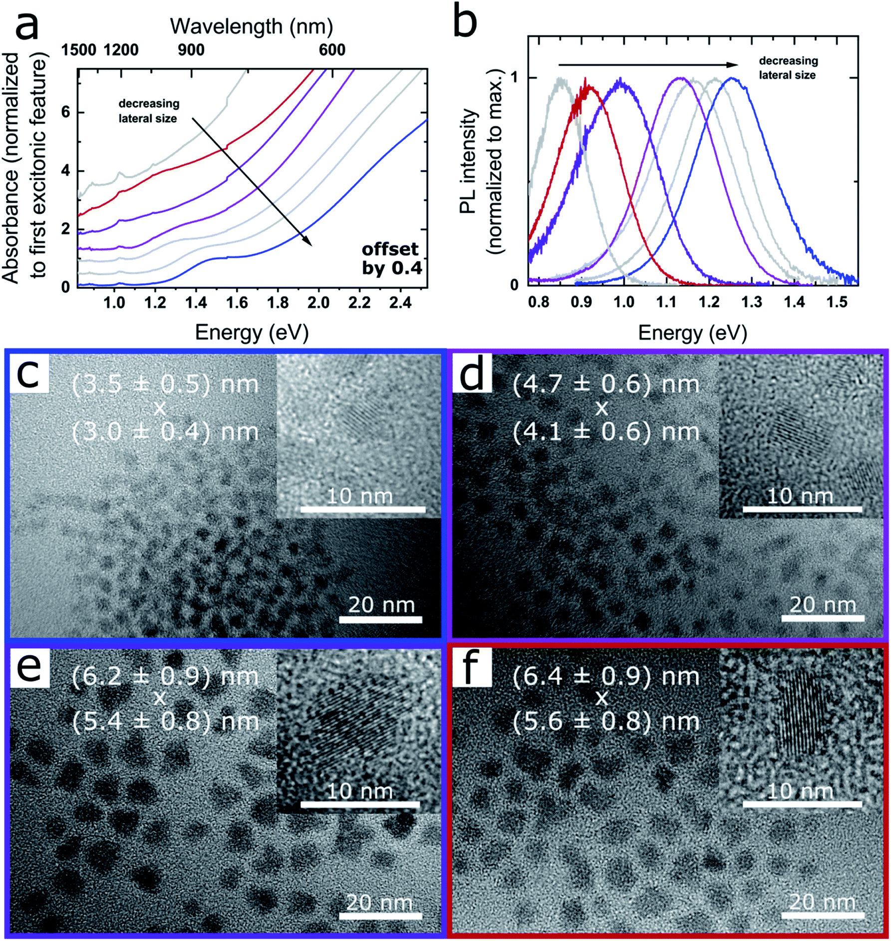 | ||
| Fig. 1 Optical properties and TEM images of CdCl2 treated PbSe NPLs. (a) Absorbance, successive spectra are plotted with an offset of 0.4 for clarity and (b) associated PL of PbSe NPLs exhibiting excitonic features in the range of 800–1000 nm, and PL between 900–1450 nm. (c)–(f) TEM images of PbSe NPLs with associated absorption and PL shown in (a) and (b). The lateral size of the NPLs in x and y-direction is shown as overlay. PbSe NPLs exhibit a narrow lateral size distribution, with the inset showing single crystalline NPLs in high magnification. Corresponding data sets in (a) and (b) and TEM images are color-coded. Additional properties and reaction conditions for each sample are shown in Fig. 2 and listed in Table 1. | ||
We find the influence on the lateral size of the PbSe NPLs strongly dependent on the reaction temperature and the amount of OcAm used for the synthesis. While a low reaction temperature (0 °C) and a low amount of OcAm present during reaction is favorable for the formation of smaller PbSe NPLs, an increase of the temperature (to room temperature) and/or of the amount of OcAm leads to larger lateral NPL sizes and a tunable red shift of their absorption and PL features (see Fig. 1b). An influence on the reaction kinetics, which are affected by the temperature and the strong interaction between the amine and the lead ions, likely leads to the observed spectral tunability.2,42 For example, Buhro and co-workers used OcAm to dissolve CdX2 precursors at room temperature, forming (CdSe)13 nanoclusters between amine double layers, which in turn yielded 2D nanobelts upon heating.32 A similar soft template mechanism is assumed to be occurring in our case. Additionally, the interaction between OcAm and HOA leads to the formation of an ammonium species, with the equilibrium of this reaction determined by the OcAM/HOA ratio and the temperature.37 However, we did not find an influence of the amount of HOA or the ratio between HOA and OcAm on the optical properties of the obtained PbSe NPLs (see open and closed circle in Fig. 2b), and consider the role of the OcAm/HOA mixture is needed in our case to ensure dissolving of the precursors. Please note that a small amount of OcAm (167 μL) and HOA (19 μL) is always present during reaction due to the addition of the selenium precursor solution, and in the following description only additional amounts of OcAm and HOA added by the Pb(OA)2 precursor solution is stated.
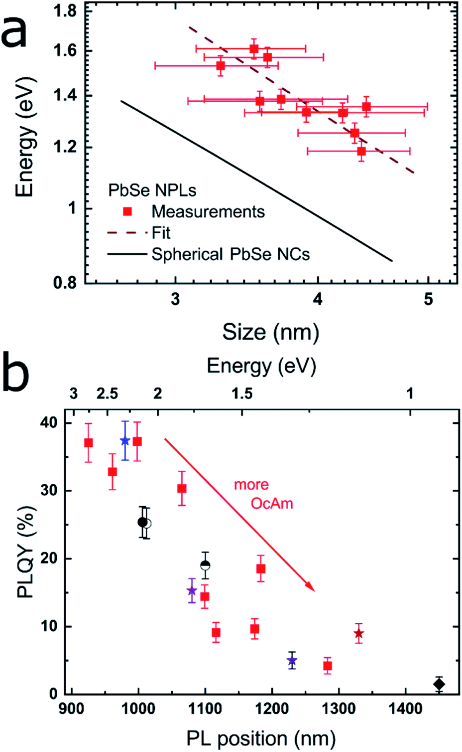 | ||
| Fig. 2 Correlation between the band gap energy and lateral size of the PbSe NPLs, as well as between the PLQY and the PL maximum. (a) Position of the first excitonic transition vs. the lateral NPL size averaged over their x- and y-dimension as determined by the TEM images. The black line is an empirical fit for PbSe NCs published by Dai et al.,44 while the dashed red line represents the fit to the PbSe NPLs which exhibit considerable additional confinement due to their 2D structure. (b) PLQY and PL position of different PbSe NPLs with red squares representing a reaction series with increasing OcAm amount, while retaining the total reaction volume as well as all other synthesis parameters. The results of the different synthesis conditions are represented by varying symbols and colors described in Table 1. | ||
By plotting the excitonic absorption of the PbSe NPLs vs. their average edge length in Fig. 2a, we find the expected decreasing band gap energy with increasing NPL size.43 The excitonic features of PbSe NPLs grow less distinct with increasing lateral NPL sizes due to an increased lateral size distribution, thus the 2nd derivate of the absorption was used for the plot as is described in the ESI (see Fig. S5†). Generally, an increase in the absorption width is found in larger NPLs as the absorption and PL is influenced by the lateral size of the NPLs rather than their thickness. We compare the obtained values with literature data for PbSe NCs expressed by an empirical sizing curve by Dai et al.44 shown in Fig. 2a,
| ΔE = 4.41/(DNCs + 0.51) | (1) |
Clearly evident, we find the values for PbSe NPLs with a certain lateral size diverging toward higher energies than PbSe NCs with comparable diameters, which underpins the confinement in the thickness of the NPLs. The hyperbolic empirical fit for PbSe NCs is explained by the highly nonparabolic curvature of the conduction and valence band near the L point in lead chalcogenides and shows good agreement with both lead chalcogenide NCs and NPLs.3,44–47
We adopt a model by Kasowski et al.48 and fit our data according to
| ΔE = (Eg2 + 2ℏ2Eg(π/0.5DNPLs)2/m*)1/2 | (2) |
 . An effective mass of m* = 0.060 ± 0.002 me exhibits the best fit in good agreement with literature values for PbSe NPLs reporting an effective mass of 0.077 me.3 The hyperbolic fit is given for both, 3D NCs and quantum wells in literature, allowing us to use the effective mass as the only variable in the Kasowski model and thus reducing the risk of overfitting.46,48 While the lateral size of the PbSe NPLs is averaged over the width and length of the NPLs for this fit, we find the higher energy for the NPLs in comparison to spherical PbSe NCs of similar diameter also occurs when only plotting the longer or the shorter lateral edge length (see Fig. S6†).
While lateral confinement has been observed in CdSe and PbS NPLs,26,50,51 its influence appears significantly higher in PbSe NPLs described here, which is shown in the NPL PL which is tunable over a large spectral range (see Fig. 1b) by a rather small lateral size increases of the NPLs. This originates from the larger exciton-Bohr-radius of PbSe (46 nm) in comparison to the exciton-Bohr-radii of PbS (23 nm) or CdSe (5.8 nm).52
Exemplary NPLs emitting at 1280 nm exhibit a thickness of 0.8 ± 0.1 nm (Fig. S4†). This thickness corresponds to four atomic layers of cubic PbSe in the (100) direction. Note that the four monolayer definition of CdSe NPLs lacks application here. Zinc blende CdSe is structured by pure Cd and Se atomic layers and the term “4 ML” denotes four layers of Se and five layers of Cd, while a PbSe layer exhibits alternating Pb and Se atoms.
The PL maximum and the PLQY of CdCl2 treated samples synthesized under different reaction conditions are shown in Fig. 2b and summarized in Table 1. Low amounts of OcAm are sufficient for a successful synthesis and result in the formation of the smallest NPLs. While it is possible to obtain PbSe NPLs without OcAm addition to the Pb(OA)2 precursor, we found the highest PLQY of 37.1% for NPLs with 0.2 mL OcAm added during the reaction (see Fig. 1c and 2b, blue star). The colored stars in Fig. 2b correspond to the samples shown in Fig. 1, with associated amounts of 0.2, 1.2, 1.4 and 1.9 mL OcAm present during reaction. With increasing amount of OcAm present in the reaction, the PLQY of PbSe NPLs drops and the absorption and PL exhibit a bathochromic shift (see Fig. 2b). We attribute the decrease in the PLQY of PbSe NPLs with a larger lateral size mainly to an “energy gap law” contribution, which has been described for organic dyes and lead chalcogenide NCs.53,54 The reduced PLQY is explained by drastically faster non-radiative recombination rates in NPLs with a smaller band gap due to a decreased energy difference between trap states close to the conduction band and the band edge.54
| PL maximum (nm) | PLQY (%) | OcAm (mL) | HOA (mL) | Hex (mL) | T (°C) | |
|---|---|---|---|---|---|---|

|
980 | 37.4 | 0.2 | 0.4 | 1.8 | 0 |

|
1080 | 15.3 | 1.2 | 0.4 | 0.8 | 0 |

|
1230 | 5.0 | 1.4 | 0.4 | 0.6 | 23 |

|
1330 | 9.0 | 1.9 | 0.5 | 1.2 | 23 |

|
1450 | 1.5 | 1.8 | 0.4 | 0.2 | 35 |

|
1100 | 19.0 | 0.2 | 0.4 | 1.8 | 23 |

|
1012 | 25.2 | 0.8 | 0.7 | 0.9 | 0 |

|
1006 | 25.4 | 0.8 | 0.1 | 1.5 | 0 |
We find the lowest temperature feasible for the NPL synthesis at −8 °C since lower temperatures lead to freezing of the solvent. With temperatures at or slightly above room temperature, we obtain NPLs with excitonic absorption and emission reaching up to the telecommunication O-, E- and S-band. An example for an increase in reaction temperature with all other parameters kept constant is shown in Fig. 2b (blue star [0 °C] and semicircle [23 °C]). The PL maximum shifts bathochromically from 980 nm to 1100 nm with associated PLQY values of 37.4%, resp. 19.0%. We observe the same trend when increasing the OcAm amount in the synthesis indicating that higher PLQY values are correlated with a smaller lateral NPL size. PbSe NPLs with the smallest size (and size distribution) are obtained at reaction temperatures of 0 °C, which we kept as temperature for PbSe NPLs used in the benchmark experiments in this work.
Postsynthetic CdCl2 treatment and time-resolved spectroscopic investigation of PbSe NPLs
A drastic increase of the PbSe NPL PLQY is apparent after their postsynthetic treatment with CdCl2, which has been shown recently for NPLs and NCs.29,55–57We use ultrafast transient absorption spectroscopy (TAS) and multi-channel scaling (MCS) PL lifetime analysis for characterizing the photophysics and charge carrier dynamics of pristine and CdCl2 treated PbSe NPLs. TA spectral and time traces of PbSe NPLs with PL centered at 985 nm (1.3 eV, pristine) and 1050 nm (1.2 eV, CdCl2 treated) are exemplarily shown in Fig. 3. We exclude the formation of an alloy or CdSe shell growth on PbSe NPLs during the metal halide treatment since reaction temperatures of 0 °C and room temperature are rather low (see Fig. 4a for comparison).57,58
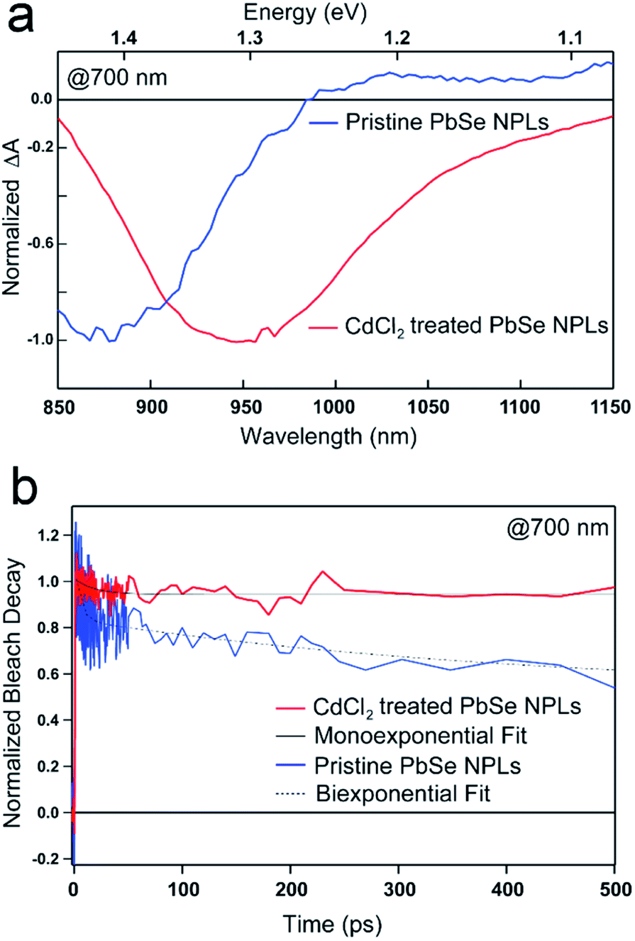 | ||
| Fig. 3 TA spectra of PbSe NPLs emitting at 985 nm and 1050 nm, resp. and photoexcited at 700 nm. (a) Spectral line cuts of pristine (blue) and CdCl2 treated (red) PbSe NPLs at a delay time of 10 ps after photoexcitation with the samples exhibiting a prominent bleach feature at 880 nm (pristine) and 950 nm (CdCl2 treated), resp. (b) Exciton dynamics of the pristine (blue) and CdCl2 treated (red) PbSe NPLs show a decay over the course of the measurement with transients of the pristine samples decaying biexponentially, while CdCl2 treated samples exhibit single exponential decay dynamics. | ||
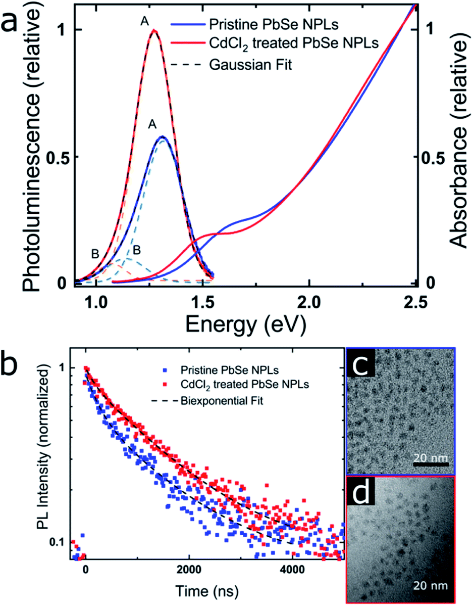 | ||
| Fig. 4 PbSe NPL PL properties (emitting at 940 nm [pristine] and 980 nm [CdCl2 treated]) (a) PL and absorbance. The PL data was corrected for the transformation from the wavelength to the energy scale by a Jacobian transformation.69 The dashed lines represent a fit of the PL with the sum of two Gaussian. (b) MCS PL lifetime measurements, taken at each PL maximum and exhibiting a biexponential decay with increasing contribution of the longer lifetime after the CdCl2 treatment. (c) and (d) TEM images of the pristine and CdCl2 treated NPLs showing a slight NPL size increase after the treatment. | ||
PbSe NPL samples were photoexcited at 700 nm (with an optical density of sample solutions of ≤0.1) and with comparable photoexcitation fluence (30 μJ cm−2) to ensure a similar distribution of the number of photoexcited excitons in pristine and CdCl2 treated PbSe NPL samples.29 TA spectral line cuts at 10 ps after photoexcitation shown in Fig. 3a exhibit a prominent ground state bleach (GSB) feature due to state filling and stimulated emission centered at 880 nm for the pristine, and 950 nm for the CdCl2 treated NPLs, respectively.59 Generally, the GSB of PbSe NPLs is slightly blue-shifted with respect to the steady-state absorption by a biexcitonic shift.59 Due to the initial fast cooling of hot charges (photoexcitation at 700 nm, above the NPL band edge, see Fig. S7† for absorption and Fig. S8† for color-coded 2D spectra), a short-lived induced absorption is probed, which decays within the first 2 ps of the measurement. After the CdCl2 treatment, the GSB of PbSe NPLs is red-shifted by 70 nm (100 meV) and hence following the same trend as the steady-state absorption and emission of the NPLs. Spectral line cuts taken at short (1 ps) and longer (3.5 ns) times after photoexcitation (Fig. S9†) underpin changes in the GSB feature of PbSe NPLs mainly at their emission wavelengths (985 nm and 1050 nm) over the course of the measurement. We find the bleach contribution of pristine PbSe NPLs at 985 nm to have significantly decayed after 3.5 ns, while CdCl2 treated samples still exhibit a considerably higher contribution at 1050 nm after 3.5 ns. This is in good agreement with the measured significantly higher PLQY values of CdCl2 treated samples (2.3% prior to and 35.3% after the treatment). Fig. 3b depicts the exciton decay dynamics of PbSe NPLs with the GSB features of pristine and CdCl2 treated PbSe NPLs being long-lived generally (exceeding the measurement time window of 6 ns, Fig. S8†), which is well in accordance with the PLQY found for both samples. Decay dynamics of photoexcited pristine PbSe NPLs are fitted biexponentially (τ1bleach = 5.5 ± 1.5 ps, τ2bleach = 400 ± 160 ps), while CdCl2 treated samples can be described with a single exponential decay (τ1bleach = 19 ± 4 ps). Although the ultrafast exciton decay dynamics of PbSe NPLs shown in Fig. 3b lack direct comparability with the PL lifetime measurements carried out (ps to ns timescales considered by TAS in comparison to tens of ns to μs timescales considered by time-resolved PL), they underpin that already at ultrafast time scales (1 ps to 6 ns), the contribution of multiple relaxation pathways gets apparent in pristine PbSe NPLs (see Fig. 3b), while one relaxation pathway seems to be effective in CdCl2 treated PbSe NPLs at early times after photoexcitation.
PL contributions
The absorption and PL spectra of PbSe NPLs and associated TEM images before and after the CdCl2 treatment are shown in Fig. 4 (size histograms in Fig. S10†). We find two components contributing to the PL lifetime, which is apparent from the slightly asymmetric shape of the PbSe NPL PL (Fig. 4a) and has been described for PbS and PbSe NCs.60,61 We fit the PL spectra with the sum of two Gaussian29,62,63 and the Gaussian centered at higher energy (labeled A) is ascribed to the PbSe band gap associated PL, while the lower energy PL (labeled B) is related to surface traps.63The PL lifetimes of PbSe NPLs (Fig. 4b and Table 2) are fitted biexponentially with the same time constants τ1PL = 168 ns and τ2PL = 1320 ns. These values are slightly longer than lifetimes typically found for PbSe NCs (∼100–1000 ns) but shorter than lifetimes measured for PbSe NPLs synthesized by cation exchange and comparable thickness (0.7–2.7 μs).20,64–66 For fitting the data, the PL lifetime of the CdCl2 treated PbSe NPLs was run freely, and the pristine sample was fitted using fixed lifetime parameters with both components exhibiting good residual (R2 = 0.98 and R2 = 0.97, resp.). After the CdCl2 treatment however, we find the contribution of the faster time constant significantly reduced from 40% to 15% (Table 2), associated with an increase of the slower time constant to 85% (Table 2). We assign these contributions to two radiative processes present in the PbSe NPL PL, with the faster time constant related to surface trap state emission and the slower time constant related to exciton recombination. The decrease of the contribution of τ1PL leads to an increase in the PL lifetime and PLQY of the PbSe NPLs, rendering the CdCl2 surface treatment successful in fixing surface-related trap states.54,67 To assign the time constants extracted from the PL lifetime measurements to their respective PL contribution, we exemplary determine the PL lifetimes at the maxima of each Gaussian fitted (see Fig. S11 and Table S1†) and find a biexponential decay, with different contributions of the two constants to the respective PL decay. The shorter PL lifetime constant (τ1PL = 168 ns) shows higher contribution at the maximum of peak B and is thus assigned to the trap state related emission, while the longer PL lifetime constant (τ2PL = 1320 ns) is dominant at peak A and is assigned to the excitonic emission. Even for pristine PbSe NPLs, the trap state emission shows a small contribution, while the PL is dominated by the band gap transition (ratio A:B 6.5:1). After the CdCl2 treatment, this effect is further enhanced as is shown by the peak area ratio of feature A (ratio A:B increasing to 22:1, see Table 3). The FWHM of the excitonic PL peak A decreases slightly from 221 to 214 meV after the CdCl2 treatment, while the FWHM of the PL peak B is significantly reduced from 217 meV to 149 meV (Fig. 4a) further underpinning the positive effect of the CdCl2 treatment. All PbSe NPL samples synthesized in this work follow this trend, and a FWHM of 180–220 meV is representative for the NPL PL, independent of the respective PL maximum (Table S2†). The FWHM of PbSe NPLs synthesized here are slightly broader than FWHM typically obtained for PbSe NCs (50–150 meV) that exhibit a band gap below 1.5 eV as well as PbSe NPLs synthesized by cation exchange (PL at 0.93 eV, FWHM of 116 meV for contribution A).20,63,68 We attribute the PL FWHM values of the PbSe NPLs shown here mainly to their lateral size distribution. However, PbS and PbSe NCs generally exhibit tunable emission with decreasing PLQY values for increasing NC sizes.68 For example, while the PLQY for small PbSe NCs with a band gap > 1.3 eV reaches 60%, NCs with a band gap < 1.2 eV have a PLQY of less than 40%.54,68 This renders our PbSe NPLs superior at shorter wavelengths (higher energy) where their PLQY values match or even exceed the PLQY of small PbSe NCs.
| PbSe NPLs | τ 1PL (ns) | A 1 (%) | τ 2PL (ns) | A 2 (%) |
|---|---|---|---|---|
| Pristine | 168 | 40 | 1320 | 60 |
| CdCl2 treated | 168 | 15 | 1320 | 85 |
| PbSe NPLs | Peak center (eV) | FWHM (meV) | Peak area | Peak ratio | |||
|---|---|---|---|---|---|---|---|
| A | B | A | B | A | B | A:B |
|
| Pristine | 1.32 | 1.14 | 221 | 217 | 0.13 | 0.02 | 6.5 |
| CdCl2 treated | 1.27 | 1.07 | 214 | 149 | 0.22 | 0.01 | 22.0 |
TEM images shown in Fig. 4c and d (as well as Fig. 1) underpin the lack of a NPL shape transformation upon CdCl2 treatment. A small lateral size increase (from 3.6 × 3.1 nm2 to 4.2 × 3.5 nm2) is apparent, which is also shown in the redshift of the NPL absorption after the treatment. The slight increase in lateral size assumedly originates from the additional reaction time after the CdCl2 treatment of the pristine NPLs. However, a change in the thickness of the NPLs or a release of lattice strain by the CdCl2 treatment cannot be ruled out completely and has been e.g. observed for CdSe NPLs.70–72 The CdCl2 treatment of PbSe NPLs is accompanied by a significant increase of the PLQY with the highest value determined for NPLs with an emission maximum of 1.27 eV (980 nm) from 14.7% before to 37.4%. Excitation spectra shown in Fig. S12† additionally support the absence of a contribution of spherical PbSe NCs as side products in the synthesis to the NPL PL. To assess the impact of the CdCl2 treatment on the PbS NPL surface, the relationship between the PLQY and the trap state density is considered as inversely linear, i.e. halving the trap state density results in a doubling of the PLQY.55,73 We conclude that nearly half of the initial surface traps in pristine PbSe NPLs emitting at 1.27 eV (980 nm) are saturated by the CdCl2 treatment. As described in the discussion of Fig. 2b, an explanation for the decreased PLQY in larger PbSe NPLs with smaller band gaps is given by the “energy gap law” contribution, leading to increased non-radiative recombination rates due to a decreased trap state and band edge energy difference.53,54 This contribution has to be considered for the CdCl2 treatment and PLQY of larger PbSe NPLs.
The chemical composition of the PbSe NPLs was determined by EDXS (see Table S3†). We find that the NPLs exhibit a slight Pb excess before and after the CdCl2 treatment, which is typical for PbSe NCs (Pb:Se ratio 1.2:1).74 The optical properties of PbSe NPLs shown in Fig. 4c and d only indicate small changes in the NPL lateral size, which is supported by the TEM images. Furthermore, after the CdCl2 treatment EDXS results show a Cd:Cl ratio of 1.8:1, closely resembling the molecular composition of CdCl2. This indicates CdCl2 acting as Z-type ligand for stabilizing PbSe NPLs.43 However, chloride anions could also act as X-type ligands, providing charge neutrality to the NPLs.55,56
Conclusions
In conclusion, we have shown the first low temperature direct colloidal synthesis of PbSe NPLs with distinct excitonic absorption features in the range of 1.55–1.24 eV (800–1000 nm). The optical properties of the NPLs are tuned by controlling their lateral dimension with the addition of octylamine and the reaction temperature, with increasing octylamine amount and higher reaction temperatures yielding larger NPLs. An efficient infrared PL of PbSe NPLs with QY values of up to 37.4% between 1.38–0.86 eV (900–1450 nm) is obtained by their postsynthetic treatment with CdCl2. Transient absorption and time-resolved PL spectroscopy reveal a considerable decrease of surface related trap states and non-radiative recombination in the PbSe NPLs by the treatment, rendering them efficient colloidal quantum emitters at telecommunication wavelengths.Conflicts of interest
There are no conflicts to declare.Acknowledgements
J. H. gratefully acknowledges financial support by the Deutsche Forschungsgemeinschaft (DFG, German Research Foundation) under Germany's Excellence Strategy -EXC-2123 QuantumFrontiers - 390837967 and HU 1318/4-1. L. K., L. B. and J. L. gratefully acknowledge funding by the Deutsche Forschungsgemeinschaft (DFG, German Research Foundation) under Germany's Excellence Strategy within the Cluster of Excellence PhoenixD (EXC 2122, Project ID 390833453). J. L. is thankful for additional funding by the Caroline Herschel program of the Leibniz Universität Hannover. The authors thank the Laboratory for Nano and Quantum Engineering (LNQE) in Hannover for access to the TEM. We thank Nadja C. Bigall for access to the photoluminescence spectrometer and Dirk Dorfs for access to the UV-Vis-NIR absorption spectrometer. We are grateful to Armin Feldhoff for providing the XRD facilities.Notes and references
- C. Schliehe, B. H. Juarez, M. Pelletier, S. Jander, D. Greshnykh, M. Nagel, A. Meyer, S. Foerster, A. Kornowski, C. Klinke and H. Weller, Science, 2010, 329, 550–553 CrossRef CAS PubMed.
- Q. A. Akkerman, B. Martín-García, J. Buha, G. Almeida, S. Toso, S. Marras, F. Bonaccorso, U. Petralanda, I. Infante and L. Manna, Chem. Mater., 2019, 31, 8145–8153 CrossRef CAS.
- W.-K. Koh, N. K. Dandu, A. F. Fidler, V. I. Klimov, J. M. Pietryga and S. V. Kilina, J. Am. Chem. Soc., 2017, 139, 2152–2155 CrossRef CAS PubMed.
- Z. Jiang, G. B. Bhandari, S. M. Premathilaka, S. Khan, D. M. Dimick, C. Stombaugh, A. Mandell, Y. He, H. Peter Lu and L. Sun, Phys. Chem. Chem. Phys., 2015, 17, 23303–23307 RSC.
- K. D. Desmet, D. A. Paz, J. J. Corry, J. T. Eells, M. T. T. Wong-Riley, M. M. Henry, E. V. Buchmann, M. P. Connelly, J. V. Dovi, H. L. Liang, D. S. Henshel, R. L. Yeager, D. S. Millsap, J. Lim, L. J. Gould, R. Das, M. Jett, B. D. Hodgson, D. Margolis and H. T. Whelan, Photomed. Laser Surg., 2006, 24, 121–128 CrossRef CAS PubMed.
- F. Koch, S. V. Chernikov and J. R. Taylor, Opt. Commun., 2000, 175, 209–213 CrossRef CAS.
- M. M. R. Moayed, T. Bielewicz, M. S. Zoellner, C. Herrmann and C. Klinke, Adv. Photonics, 2017 DOI:10.1364/noma.2017.NoTu1C.3.
- M. Aerts, T. Bielewicz, C. Klinke, F. C. Grozema, A. J. Houtepen, J. M. Schins and L. D. A. Siebbeles, Nat. Commun., 2014, 5, 3789 CrossRef PubMed.
- S. Dogan, T. Bielewicz, Y. Cai and C. Klinke, Appl. Phys. Lett., 2012, 101, 73102 CrossRef.
- J. Lauth, M. Failla, E. Klein, C. Klinke, S. Kinge and L. D. A. Siebbeles, Nanoscale, 2019, 11, 21569–21576 RSC.
- T. Bielewicz, S. Dogan and C. Klinke, Small, 2015, 11, 826–833 CrossRef CAS PubMed.
- Z. Chen, B. Nadal, B. Mahler, H. Aubin and B. Dubertret, Adv. Funct. Mater., 2014, 24, 295–302 CrossRef CAS.
- M. Bernardi, M. Palummo and J. C. Grossman, Nano Lett., 2013, 13, 3664–3670 CrossRef CAS PubMed.
- S. Dogan, T. Bielewicz, V. Lebedeva and C. Klinke, Nanoscale, 2015, 7, 4875–4883 RSC.
- S. Krishnamurthy, A. Singh, Z. Hu, A. V. Blake, Y. Kim, A. Singh, E. A. Dolgopolova, D. J. Williams, A. Piryatinski, A. V. Malko, H. Htoon, M. Sykora and J. A. Hollingsworth, ACS Nano, 2021, 15, 575–587 CrossRef CAS PubMed.
- C. J. Hanson, N. F. Hartmann, A. Singh, X. Ma, W. J. I. DeBenedetti, J. L. Casson, J. K. Grey, Y. J. Chabal, A. V. Malko, M. Sykora, A. Piryatinski, H. Htoon and J. A. Hollingsworth, J. Am. Chem. Soc., 2017, 139, 11081–11088 CrossRef CAS PubMed.
- F. Xu, X. Ma, Q. Zhang, H.-K. Lo and J.-W. Pan, Rev. Mod. Phys., 2020, 92(2), 025002 CrossRef CAS.
- X. Cao, M. Zopf and F. Ding, J. Semicond., 2019, 40, 71901 CrossRef CAS.
- S. M. Tenney, V. Vilchez, M. L. Sonnleitner, C. Huang, H. C. Friedman, A. J. Shin, T. L. Atallah, A. P. Deshmukh, S. Ithurria and J. R. Caram, J. Phys. Chem. Lett., 2020, 11, 3473–3480 CrossRef CAS PubMed.
- T. Galle, M. Samadi Khoshkhoo, B. Martin-Garcia, C. Meerbach, V. Sayevich, A. Koitzsch, V. Lesnyak and A. Eychmüller, Chem. Mater., 2019, 31, 3803–3811 CrossRef CAS.
- T. Galle, D. Spittel, N. Weiß, V. Shamraienko, H. Decker, M. Georgi, R. Hübner, N. Metzkow, C. Steinbach, D. Schwarz, V. Lesnyak and A. Eychmüller, J. Phys. Chem. Lett., 2021, 12, 5214–5220 CrossRef CAS PubMed.
- S. Ithurria, M. D. Tessier, B. Mahler, R. P. S. M. Lobo, B. Dubertret and A. L. Efros, Nat. Mater., 2011, 10, 936–941 CrossRef CAS PubMed.
- A. D. Antu, Z. Jiang, S. M. Premathilka, Y. Tang, J. Hu, A. Roy and L. Sun, Chem. Mater., 2018, 30, 3697–3703 CrossRef CAS.
- H. Zhang, B. H. Savitzky, J. Yang, J. T. Newman, K. A. Perez, B.-R. Hyun, L. F. Kourkoutis, T. Hanrath and F. W. Wise, Chem. Mater., 2016, 28, 127–134 CrossRef CAS.
- D. D. Vaughn, R. J. Patel, M. A. Hickner and R. E. Schaak, J. Am. Chem. Soc., 2010, 132, 15170–15172 CrossRef CAS PubMed.
- P. J. Morrison, R. A. Loomis and W. E. Buhro, Chem. Mater., 2014, 26, 5012–5019 CrossRef CAS.
- A. H. Khan, S. Pal, A. Dalui, J. Pradhan, D. D. Sarma and S. Acharya, Chem. Mater., 2017, 29, 1175–1182 CrossRef CAS.
- A. H. Khan, R. Brescia, A. Polovitsyn, I. Angeloni, B. Martín-García and I. Moreels, Chem. Mater., 2017, 29, 2883–2889 CrossRef CAS.
- F. Manteiga Vázquez, Q. Yu, L. F. Klepzig, L. D. A. Siebbeles, R. W. Crisp and J. Lauth, J. Phys. Chem. Lett., 2021, 12, 680–685 CrossRef PubMed.
- Y. Chen, D. Chen, Z. Li and X. Peng, J. Am. Chem. Soc., 2017, 139, 10009–10019 CrossRef CAS PubMed.
- Y. Zhou, M. Celikin, A. Camellini, G. Sirigu, X. Tong, L. Jin, K. Basu, D. Barba, D. Ma, S. Sun, F. Vidal, M. Zavelani-Rossi, Z. M. Wang, H. Zhao, A. Vomiero and F. Rosei, Adv. Energy Mater., 2017, 7, 1602728 CrossRef.
- Y.-H. Liu, F. Wang, Y. Wang, P. C. Gibbons and W. E. Buhro, J. Am. Chem. Soc., 2011, 133, 17005–17013 CrossRef CAS PubMed.
- J. S. Son, X.-D. Wen, J. Joo, J. Chae, S.-I. Baek, K. Park, J. H. Kim, K. An, J. H. Yu, S. G. Kwon, S.-H. Choi, Z. Wang, Y.-W. Kim, Y. Kuk, R. Hoffmann and T. Hyeon, Angew. Chem., Int. Ed., 2009, 48, 6861–6864 CrossRef CAS PubMed.
- A. Riedinger, F. D. Ott, A. Mule, S. Mazzotti, P. N. Knüsel, S. J. Kress, F. Prins, S. C. Erwin and D. J. Norris, Nat. Mater., 2017, 16, 743–748 CrossRef CAS PubMed.
- M. P. Campos, M. P. Hendricks, A. N. Beecher, W. Walravens, R. A. Swain, G. T. Cleveland, Z. Hens, M. Y. Sfeir and J. S. Owen, J. Am. Chem. Soc., 2017, 139, 2296–2305 CrossRef CAS PubMed.
- J. S. Owen, E. M. Chan, H. Liu and A. P. Alivisatos, J. Am. Chem. Soc., 2010, 132, 18206–18213 CrossRef CAS PubMed.
- G. Almeida, L. Goldoni, Q. Akkerman, Z. Dang, A. H. Khan, S. Marras, I. Moreels and L. Manna, ACS Nano, 2018, 12, 1704–1711 CrossRef CAS PubMed.
- M. P. Hendricks, M. P. Campos, G. T. Cleveland, I. Jen-La Plante and J. S. Owen, Science, 2015, 348, 1226–1230 CrossRef CAS PubMed.
- J. Lauth, G. Grimaldi, S. Kinge, A. J. Houtepen, L. D. A. Siebbeles and M. Scheele, Angew. Chem., Int. Ed., 2017, 56, 14061–14065 CrossRef CAS PubMed.
- F. C. M. Spoor, L. T. Kunneman, W. H. Evers, N. Renaud, F. C. Grozema, A. J. Houtepen and L. D. A. Siebbeles, ACS Nano, 2016, 10, 695–703 CrossRef CAS PubMed.
- J. A. McGuire, J. Joo, J. M. Pietryga, R. D. Schaller and V. I. Klimov, Acc. Chem. Res., 2008, 41, 1810–1819 CrossRef CAS PubMed.
- Y. Wang, Y. Zhou, Y. Zhang and W. E. Buhro, Inorg. Chem., 2015, 54, 1165–1177 CrossRef CAS PubMed.
- A. I. Ekimov and A. A. Onushchenko, JETP Lett., 1981, 34, 345–348 Search PubMed.
- Q. Dai, Y. Wang, X. Li, Y. Zhang, D. J. Pellegrino, M. Zhao, B. Zou, J. Seo, Y. Wang and W. W. Yu, ACS Nano, 2009, 3, 1518–1524 CrossRef CAS PubMed.
- I. Kang and F. W. Wise, J. Opt. Soc. Am. B, 1997, 14, 1632 CrossRef CAS.
- G. Allan and C. Delerue, Mater. Sci. Eng., C, 2005, 25, 687–690 CrossRef.
- F. C. M. Spoor, G. Grimaldi, C. Delerue, W. H. Evers, R. W. Crisp, P. Geiregat, Z. Hens, A. J. Houtepen and L. D. A. Siebbeles, ACS Nano, 2018, 12, 4796–4802 CrossRef CAS PubMed.
- Y. Wang, A. Suna, W. Mahler and R. Kasowski, J. Chem. Phys., 1987, 87, 7315–7322 CrossRef CAS.
- In Non-Tetrahedrally Bonded Elements and Binary Compounds I, O. Madelung, U. Rössler and M. Schulz, Springer-Verlag, Berlin/Heidelberg, 1998, pp. 1–8 Search PubMed.
- S. Ithurria, G. Bousquet and B. Dubertret, J. Am. Chem. Soc., 2011, 133, 3070–3077 CrossRef CAS PubMed.
- G. H. V. Bertrand, A. Polovitsyn, S. Christodoulou, A. H. Khan and I. Moreels, Chem. Commun., 2016, 52, 11975–11978 RSC.
- L. Brus, J. Phys. Chem., 1986, 90, 2555–2560 CrossRef CAS.
- H. C. Friedman, E. D. Cosco, T. L. Atallah, S. Jia, E. M. Sletten and J. R. Caram, Chem, 2021, 7(12), 3359–3376 CAS.
- O. E. Semonin, J. C. Johnson, J. M. Luther, A. G. Midgett, A. J. Nozik and M. C. Beard, J. Phys. Chem. Lett., 2010, 1, 2445–2450 CrossRef CAS.
- N. Kirkwood, J. O. V. Monchen, R. W. Crisp, G. Grimaldi, H. A. C. Bergstein, I. Du Fossé, W. van der Stam, I. Infante and A. J. Houtepen, J. Am. Chem. Soc., 2018, 140, 15712–15723 CrossRef CAS PubMed.
- M. Dufour, J. Qu, C. Greboval, C. Méthivier, E. Lhuillier and S. Ithurria, ACS Nano, 2019, 13, 5326–5334 CrossRef CAS PubMed.
- W. K. Bae, J. Joo, L. A. Padilha, J. Won, D. C. Lee, Q. Lin, W.-K. Koh, H. Luo, V. I. Klimov and J. M. Pietryga, J. Am. Chem. Soc., 2012, 134, 20160–20168 CrossRef CAS PubMed.
- P. B. Green, Z. Li and M. W. Wilson, J. Phys. Chem. Lett., 2019, 10, 5897–5901 CrossRef CAS PubMed.
- J. M. Schins, M. T. Trinh, A. J. Houtepen and L. D. A. Siebbeles, Phys. Rev. B: Condens. Matter Mater. Phys., 2009, 80(3), 03523 CrossRef.
- J. M. Harbold and F. W. Wise, Phys. Rev. B: Condens. Matter Mater. Phys., 2007, 76(12), 125304 CrossRef.
- J. R. Caram, S. N. Bertram, H. Utzat, W. R. Hess, J. A. Carr, T. S. Bischof, A. P. Beyler, M. W. B. Wilson and M. G. Bawendi, Nano Lett., 2016, 16, 6070–6077 CrossRef CAS PubMed.
- O. Erdem, M. Olutas, B. Guzelturk, Y. Kelestemur and H. V. Demir, J. Phys. Chem. Lett., 2016, 7, 548–554 CrossRef CAS PubMed.
- I. Skurlov, A. Sokolova, T. Galle, S. Cherevkov, E. Ushakova, A. Baranov, V. Lesnyak, A. Fedorov and A. Litvin, Nanomaterials, 2020, 10(12), 2570 CrossRef CAS PubMed.
- J. M. An, A. Franceschetti and A. Zunger, Nano Lett., 2007, 7, 2129–2135 CrossRef CAS.
- M. Sykora, A. Y. Koposov, J. A. McGuire, R. K. Schulze, O. Tretiak, J. M. Pietryga and V. I. Klimov, ACS Nano, 2010, 4, 2021–2034 CrossRef CAS PubMed.
- A. Kigel, M. Brumer, G. I. Maikov, A. Sashchiuk and E. Lifshitz, Small, 2009, 5, 1675–1681 CrossRef CAS PubMed.
- B. R. Fisher, H.-J. Eisler, N. E. Stott and M. G. Bawendi, J. Phys. Chem. B, 2004, 108, 143–148 CrossRef CAS.
- H. Lu, G. M. Carroll, N. R. Neale and M. C. Beard, ACS Nano, 2019, 13, 939–953 CAS.
- J. Mooney and P. Kambhampati, J. Phys. Chem. Lett., 2013, 4, 3316–3318 CrossRef CAS.
- N. Moghaddam, C. Dabard, M. Dufour, H. Po, X. Xu, T. Pons, E. Lhuillier and S. Ithurria, J. Am. Chem. Soc., 2021, 143, 1863–1872 CrossRef CAS PubMed.
- S. Christodoulou, J. I. Climente, J. Planelles, R. Brescia, M. Prato, B. Martín-García, A. H. Khan and I. Moreels, Nano Lett., 2018, 18, 6248–6254 CrossRef CAS PubMed.
- C. Meerbach, C. Wu, S. C. Erwin, Z. Dang, A. Prudnikau and V. Lesnyak, Chem. Mater., 2020, 32, 566–574 CrossRef CAS.
- C. Bullen and P. Mulvaney, Langmuir, 2006, 22, 3007–3013 CrossRef CAS PubMed.
- M. C. Weidman, M. E. Beck, R. S. Hoffman, F. Prins and W. A. Tisdale, ACS Nano, 2014, 8, 6363–6371 CrossRef CAS PubMed.
Footnote |
| † Electronic supplementary information (ESI) available: Complementary results, including powder X-ray diffraction, energy dispersive X-ray spectroscopy, excitation spectroscopy. See DOI: 10.1039/d1na00704a |
| This journal is © The Royal Society of Chemistry 2022 |