
 Open Access Article
 This Open Access Article is licensed under a
 Creative Commons Attribution 3.0 Unported Licence
The effect of water ingress on additively manufactured electrodes†
Rhys J.
Williams
,
Tom
Brine
,
Robert D.
Crapnell
 ,
Alejandro Garcia-Miranda
Ferrari
and
Craig E.
Banks
*
,
Alejandro Garcia-Miranda
Ferrari
and
Craig E.
Banks
*
Faculty of Science and Engineering, Manchester Metropolitan University, Chester Street, Manchester M1 5GD, UK. E-mail: c.banks@mmu.ac.uk; Tel: +441612471196
First published on 8th August 2022
Abstract
Additive Manufacturing (AM), otherwise known as 3D printing, is becoming increasingly popular in the field of electrochemistry since it allows affordable, on-demand production of bespoke devices. Provided a suitably conductive polymer composite material is used, this can include working electrodes. However, while a number of publications have shown such Additively Manufactured Electrodes (AMEs) to be effective, there remain several fundamental areas which must be understood to continue the development of AM for electrochemistry. One such area is the effect of solvent ingress on AME performance, with water probably representing the most important solvent for study considering the amount of electrochemical sensing directed towards biological and environmental systems. Therefore, in this work we study the effect of up to 28 days of water immersion on the physical properties and electrochemical performance of AMEs made from a commonly used conductive material, Protopasta. It is shown that water immersion leads to water uptake of around 1–1.5% by mass for our specific electrode design, which in turn causes a decrease in measured peak current, but an increase in the heterogeneous electron transfer rate constant, k0. These observations are rationalised in terms of Ohmic drop and conductive filler surface chemistry, respectively. Overall, it can be concluded that water ingress is likely to be a concern for any application where AMEs are expected to have extended contact with water, although we note that more work is required to fully understand the extent of the issue.
1. Introduction
Additive Manufacturing (AM), also known as 3D printing, refers to a group of manufacturing processes in which digital computer-aided design (CAD) files are processed into physical parts by building consecutive, thin-layered cross-sections until a complete 3D object has been produced. Compared to traditional formative and subtractive manufacturing processes, AM has a number of advantages, including: on-demand manufacturing, and subsequently lower waste; shorter lead times and lower costs for short production runs; a high degree of customisability, since CAD files can easily be altered, and the ability to produce complex part geometries (e.g. overhangs and nested structures).1 Such benefits have led to increasing adoption of AM technologies,1,2 and they are especially useful in laboratory settings where they can be used to produce a variety of bespoke sample holders, fixtures, and devices, all of which might otherwise be prohibitively expensive.3,4In particular, Fused Filament Fabrication (FFF) has seen widespread adoption because of the relatively low cost of FFF printers and the simplicity of their use.2 In FFF, a millimetre scale thermoplastic polymer filament is passed through a heated nozzle such that it melts and can be extruded onto a substrate where it cools and re-solidifies. Moving the nozzle horizontally during extrusion allows the production of thin cross-sections, and raising the nozzle allows extrusion of the next cross-section onto the previous, with this layer-by-layer assembly repeated until the desired 3D part has been obtained. A wide range of commercial FFF filaments are available including not only a variety of different polymers,2 but also polymer composite materials in which a filler has been added, for example to provide mechanical reinforcement or allow electrical conductivity.
Recently, polymer composite FFF filaments which conduct electricity have received particular interest in the field of electrochemistry. Although the printed filaments typically require chemical or physical surface treatments to endow optimum electrochemical properties,5 electrodes produced using FFF are nonetheless becoming increasingly popular as they represent a cheap and convenient means for the production of bespoke devices for electrochemical sensing; literature reviews by Cardoso et al.,6 Silva et al.,7 and Omar et al.8 provide a good overview of the progress of Additively Manufactured Electrodes (AMEs), and Whittingham et al.4 and Ambrosi and Bannani9 recently discussed how both AMEs and 3D printing in general can be effectively incorporated into electrochemical and analytical laboratories. However, while it is clear that AMEs are a promising use of FFF technology, there remain understudied issues in the field, one of which is the effect of solvents on the performance of the printed electrodes.
It is basic scientific knowledge that many polymers are soluble in a variety of solvents, and that a polymer which dissolves in a particular solvent would be unsuitable for 3D printed parts intended to have contact with that solvent in their working lives. However, while controlled polymer dissolution has been reported for activation of FFF electrodes,10 and efforts have recently been made to explore the usefulness of different AM materials for electrochemistry in terms of their solvent stability,11 for many electrochemists, polymer/solvent interactions have not been mentioned as a concern. This is presumably because the most commonly-used conducting filaments are made from poly(lactic acid) (PLA), which is insoluble in the aqueous samples typically of interest. Perhaps under-appreciated by electrochemists is the inherent permeability of polymer materials towards small molecules, with PLA representing a particularly poor barrier compared to other common polymers.12 Such solvent ingress often results in swelling of the polymer, which can lead to structural damage13 to and changes in bulk mechanical properties14 of the polymer. These physical changes might well prove to be of concern to electrochemists, for example because swelling could change the electroactive area of the electrodes. Perhaps more importantly, it is unknown what effect absorbed water molecules might have on the electrical properties of FFF electrodes, both in terms of the bulk conductivity of the material, and the chemical processes occurring at the electrode/analyte interface.
In order to address this, in this paper we provide the first empirical study regarding the effects of water ingress on AMEs produced using FFF and the commonly used conductive filament, Protopasta (ProtoP).6,15 More specifically, we demonstrate that over 28 days of immersion in water at room temperature, such AMEs can absorb sufficient water to cause changes in their electrochemical performance as assessed by cyclic voltammetry (CV). Overall, this work serves to demonstrate the importance of understanding polymer/solvent interactions for facilitating the further incorporation of polymer AM into the field of electrochemistry.
2. Materials and methods
2.1 Materials
All chemicals were used as received, without further purification or modification. Protoplant “Protopasta Composite Conductive PLA” (1.75 mm diameter) was purchased from Premier Farnell UK Limited. Sodium hydroxide pellets (≥97%) and hexaammineruthenium(III) chloride (98%) (RuHex) were obtained from Sigma-Aldrich, and propan-2-ol (HPLC grade, ≥99.5%) was obtained from Fisher Scientific. Deionised water was generated by a Millipore Milli-Q Integral 3 water purification unit, which dispensed water with a resistivity greater than or equal to 18 MΩ cm at 25 °C.2.2 Methods
 | ||
| Fig. 1 (A) Engineering drawing illustrating the dimensions (in mm) of the AMEs used in this work; (B) digital rendering of the AMEs arranged on the print bed in the slicer software. | ||
3. Results and discussion
3.1 Electrode activation and characterisation
The majority of electrochemistry work using AMEs is carried out after a pre-activation step to remove surface polymer and reveal subsurface conductive carbon particles, which improves electrode performance.15 Therefore, any part of the surface exposed to water ingress in most real applications is likely to be of this etched nature rather than pristine, as-printed polymer composite. To reflect this, activated ProtoP electrodes (labelled A-ProtoP) were generated by chronoamperometry in alkali solution, which has been established as an effective AME activation method.16 Unusually, almost the entire lengths of the electrodes were activated (apart from the small section held by the connecting clip), rather than the intended electroactive area alone; this was to ensure that the ingress behaviour of the A-ProtoP parts was reflective solely of activated surface, rather than a combination of a relatively small area of activated surface and relatively large area of non-activated surface.Chemical evidence for the success of the surface activation can be found by XPS. Fitting the ProtoP spectrum (Fig. 2A) is very similar to pure PLA (Fig. S1A, ESI†), with three peaks of similar intensity corresponding to the three carbon environments in the main PLA chain, and an additional adventitious carbon (Adv. C) peak which was found to persist despite cleaning of the parts before XPS analysis. The similarity of the ProtoP and PLA spectra suggests that, in non-activated ProtoP, the conductive carbon black particles are concealed below the polymer surface beyond the depth explored by XPS (i.e., a few nm). By contrast, the C 1s environment of the A-ProtoP requires the addition of an asymmetric peak centred at 284.3 eV, which is consistent with X-ray photoelectron emission by graphitic carbon,18,19 in this case carbon black. Similarly, a high binding energy peak centred at 291.8 eV is required for adequate fitting of the A-ProtoP spectrum, which arises from π–π* transitions within graphitic carbon.18,19 In both ProtoP and A-ProtoP spectra, there is a small peak centred at approximately 290–292 eV. This is difficult to assign but is speculated to arise from carboxyl groups at PLA chain ends. This peak is somewhat larger for A-ProtoP, and there is also enrichment of the region corresponding to alcohol environments for this sample, which indicate successful hydrolysis of the PLA chain during the activation reaction. This conclusion is supported further by the presence of additional environments in the O 1s spectrum of A-ProtoP (Fig. S1B, ESI†). Overall, these data show that the activation process successfully removes surface PLA to reveal conductive carbon black particles.
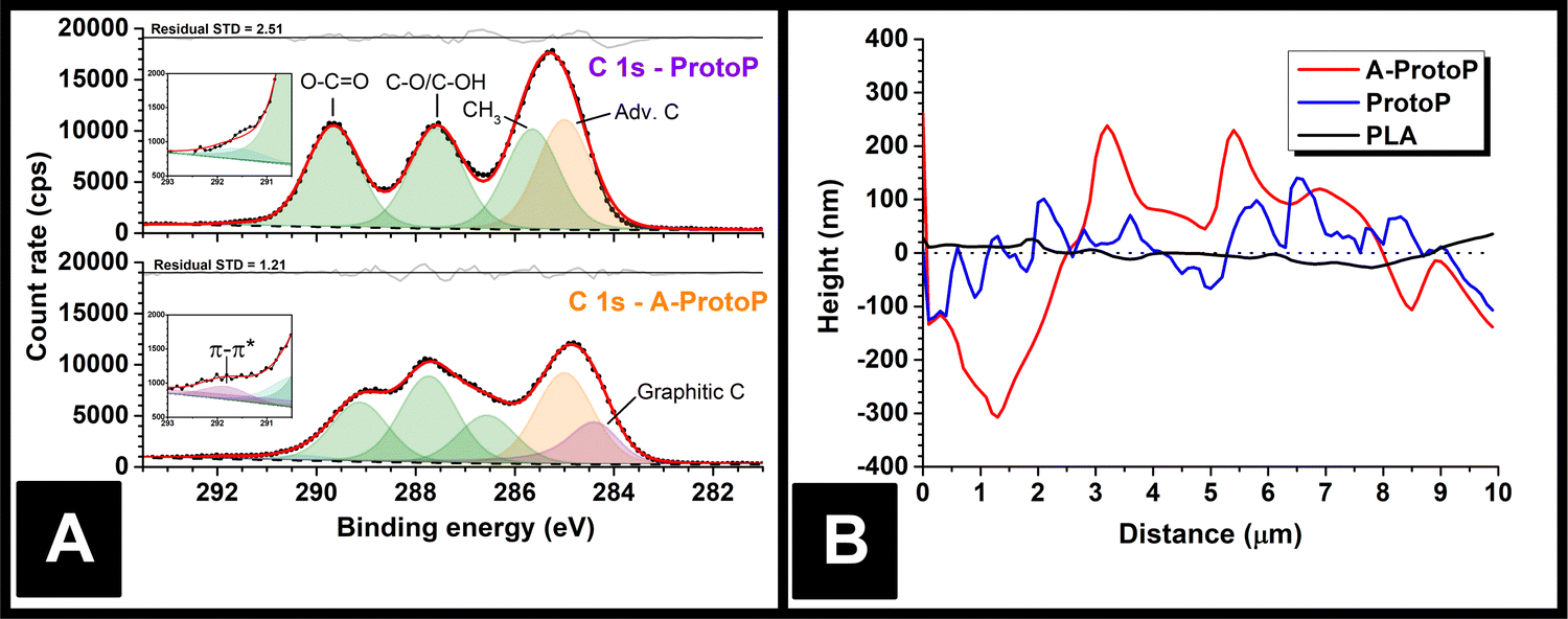 | ||
| Fig. 2 (A) XPS data for the ProtoP and A-ProtoP AMEs, which highlights the appearance of graphitic carbon at the part surface after activation; (B) AFM height profiles for PLA, ProtoP and A-ProtoP, which demonstrate the significantly increased roughness of the AMEs after activation. In order to allow for easy comparison, the height profiles in the graph have been calibrated such that mean height for all samples is zero. | ||
Physical evidence of activation can be seen by AFM of the part surfaces (Fig. 2B), which demonstrates that the A-ProtoP surface was significantly rougher than that of the ProtoP, which in turn was rougher than the pure PLA. This can be quantified in terms of a roughness factor, Ra, which is the arithmetic mean of the absolute deviations in the height measured at each point from the mean value of height calculated for the whole evaluation length.20 For A-ProtoP, ProtoP, and PLA, the calculated Ra were (119 ± 72) nm, (45 ± 38) nm, and (12 ± 9) nm, respectively (Mean ± S.D.). The increased roughness of the A-ProtoP can be attributed to the loss of polymer at the part surface as a consequence of activation. SEM images of the samples are shown in Fig. S2 (ESI†); these are of relatively low magnification, so do not give evidence of surface modification upon activation, but they do demonstrate that activation does not appear to change the macroscopic structure of the parts in a way that might significantly increase liquid uptake, e.g., by generating holes or cracks between layers.
Finally, it was found that the activation process led to an average mass increase of (0.3 ± 0.2) mg, i.e. (0.2 ± 0.1)% (Mean ± S.D.). It is therefore concluded that the activation process itself causes water ingress into the parts, which is surprising because it is carried out over a short timescale, and because one would expect removal of the polymer in the activation process to cause a reduction in part mass. Indeed, the measured mass increase is likely not as large as the total mass of water imbibed during activation because of the competing loss of polymer mass. The cause of this accelerated water ingress is speculated to be localised heating arising from a combination of resistance heating of the polymer composite under the applied potential, and thermal energy released as a consequence of the etching reaction.
3.2 Water ingress into electrodes
The lengths, thicknesses, and head diameters (Fig. 1A) of the PLA and ProtoP electrodes were measured during the course of 28 days of immersion in water. As can be seen in Fig. 3A, the changes in dimensions due to water ingress were generally small, with the largest relative variations being in thickness. The maximum increase in thickness was (0.7 ± 0.3)%, or (0.013 ± 0.004) mm, seen for the ProtoP samples at 14 days of immersion. This value is close to the instrumental precision and is not part of a wider trend, so is difficult to justify as significant. From these data, it can be concluded that any swelling of AMEs caused by water ingress is likely to be negligible. Because of this, dimensional measurements were omitted for later samples (i.e., A-ProtoP).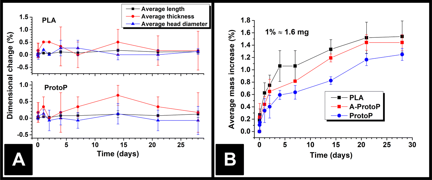 | ||
| Fig. 3 (A) AME dimensions versus time upon water immersion; (B) AME mass versus time upon water immersion. In both cases, the data points are (Mean ± S.D.) for three electrodes. | ||
The mass ingress versus time for the AMEs is shown in Fig. 3B. The initial mass of the A-ProtoP electrodes (i.e., 0% increase) is taken to be the mass after activation, not before. While it is possible to fit theoretical models of diffusion to solvent ingress versus time data,12 it is complicated significantly in this case by the semi-crystalline nature of PLA,21 the anisotropy inherent to FFF, and the non-standard, 3D shape being studied. As such, ingress data is considered here in empirical terms only. In general, the water absorption was relatively small, with mass increases at 28 days’ immersion of (1.54 ± 0.25)%, (1.44 ± 0.13)%, and (1.25 ± 0.10)% for PLA, A-ProtoP, and ProtoP, respectively (Mean ± S.D). For reference, 1% uptake corresponds to an absolute mass of approximately 1.6 mg. The trend in the rate of uptake is the same, with PLA absorbing water the fastest, followed by A-ProtoP, and ProtoP absorbing water at the slowest rate. The decreased capacity for water absorption in the ProtoP and A-ProtoP can be explained by the presence of the carbon black filler particles, which act as “dead” volume into which water cannot be imbibed, and also act as physical barriers which increase the path length for diffusion of water molecules into the material.22 The increased rate and extent over 28 days of water absorption by the A-ProtoP relative to the ProtoP is speculated to be related to its significantly rougher surface, which provides a greater contact area for liquid absorption. The differences in rate of uptake could feasibly also be due to chemical differences in the AME surfaces through which wetting and water uptake might have been enhanced. However, the most obvious means to study this would be via water contact angle measurements, the results of which are also affected by surface roughness.23 That is to say, it would be difficult to deconvolute the effects of surface chemistry from surface roughness. Furthermore, XPS results for the AMEs (Section 3.1) suggest that the differences in surface chemistry of the AMEs are not extreme, especially between PLA and ProtoP. Overall, it can be concluded that water absorption into the AMEs was small but measurable, and, similarly, that there were measurable differences between activated and non-activated electrodes, which were suspected to be due to surface roughness.
3.3 Effect of water ingress on electrochemical performance
After 28 days of immersion in water or ambient storage, as applicable, the resistances of the electrodes were measured, and these are summarised in Table 1. Non-activated samples are labelled with the prefix NA, activated samples with the prefix A, non-immersed samples with the suffix NI, and immersed samples with suffix I. For example, an activated electrode which was not immersed in water is labelled A-NI. As can be seen in Table 1, the NA-I samples had almost double the resistance of their non-immersed counterparts. By contrast, no obvious change in resistance upon water ingress was seen for the A samples, although it should be noted that the uncertainty in the A-NI value is relatively large and hence might obscure such a change. A possible cause of increasing AME resistance upon water ingress is speculated to be a change in the permittivity of the polymer material when it contains absorbed water.| Sample | Resistance/kΩ | A real/cm2 | I red.p at 50 mV s−1/μA | ΔEp/mV at 50 mV s−1 | Average k0obs./cm s−1 |
|---|---|---|---|---|---|
| NA-NI | 1.5 ± 0.2 | 0.43 ± 0.01 | −109 ± 6 | 280 ± 10 | 3.64 × 10⁻⁴ |
| NA-I | 2.7 ± 0.2 | 0.265 ± 0.005 | −55 ± 7 | 230 ± 30 | 5.75 × 10⁻⁴ |
| A-NI | 1.4 ± 0.4 | 0.61 ± 0.01 | −140 ± 7 | 330 ± 60 | 2.86 × 10⁻⁴ |
| A-I | 1.4 ± 0.1 | 0.56 ± 0.02 | −128 ± 8 | 264 ± 1 | 3.93 × 10⁻⁴ |
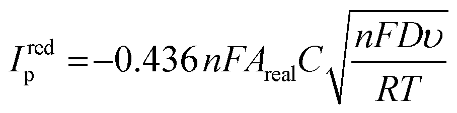
Immediately after their resistance measurement, CV data in a solution of 1 mM RuHex (in 0.1 M KCl) were obtained for the electrodes, and these data are shown Fig. 4A and B for NA and A samples, respectively. As can be seen by simple inspection of Fig. 4, both A samples showed greater reduction peak (Ired.p) currents than NA, which is a consequence of activation revealing more of the conductive filler.15,16 In the case of both NA and A samples, water ingress led to decreases in both the Ired.p currents and in the measured peak-to-peak separations (ΔEp). The average Ired.p and ΔEp measured at a scan rate of 50 mV s−1 are summarised in Table 1 for comparison. For a quasi-reversible electrochemical process such as this,24 the observed peak reduction current can be calculated using the Randles–Ševćik equation:25
 | (1) |
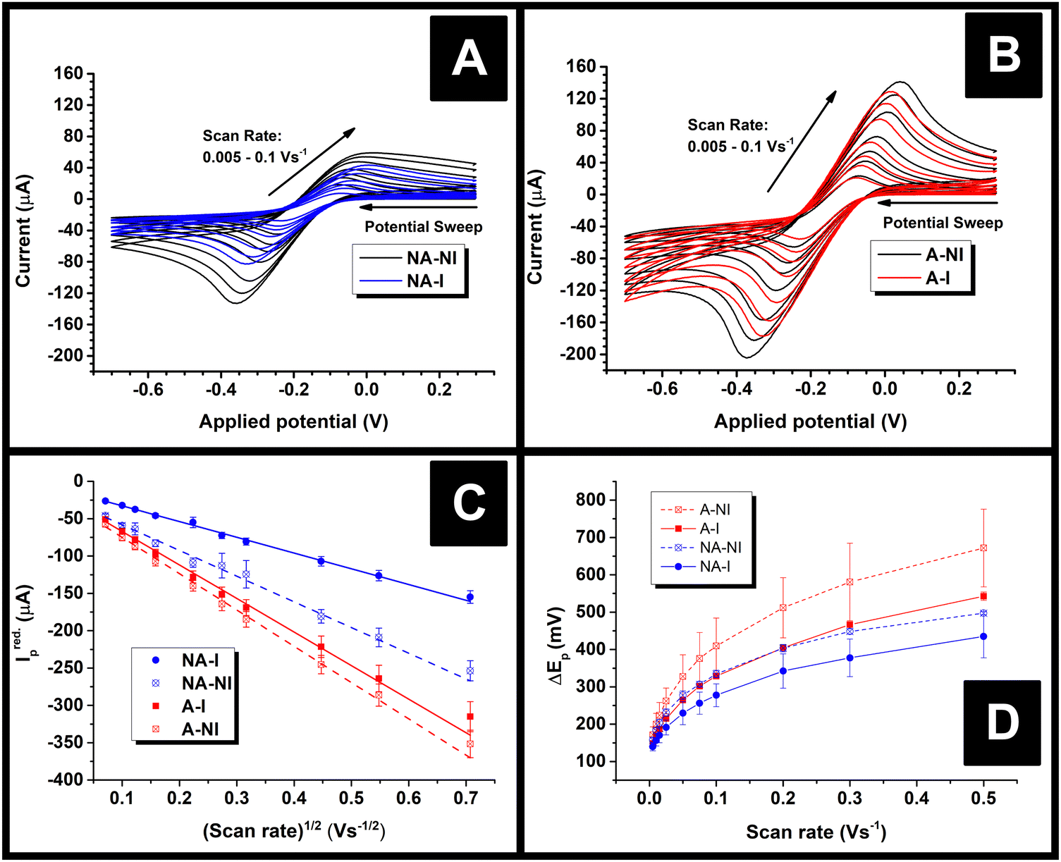 | ||
| Fig. 4 (A) CV data for example NA-AMEs; (B) CV data for example A-AMEs; (C) Randles–Ševćik plot for the AMEs based on the average data from CV; (D) average ΔEpversus scan rate for the AMEs. For (C and D), the data points are (Mean ± S.D.). | ||
In all cases, the Areal calculated using eqn (1) was lower than the theoretical area calculated from the geometry of the electrode, i.e., the surface area of a 2 mm thick, 2.5 mm radius cylinder, minus the 4 mm2 connection edge, which equals approximately 0.7 cm2. This is unexpected, since previous literature found the electroactive area of AMEs to be higher than their theoretical area, which was rationalised in terms of surface roughness increasing the true surface area of the electrode beyond that calculated from the macroscopic geometry of the electrode.24 Upon water ingress, the calculated Areal decreased for both sample types, although the decrease was much more significant for the NA samples than the A samples (38% versus 8%). The smaller decrease for the A samples is probably due to the fact that measurable water ingress was already found to occur during activation, i.e. A-NI samples are already somewhat saturated with water. It is tempting to rationalise these changes in terms of physical or chemical changes at the electrode surfaces, for example, a physical explanation for this phenomenon could be that I samples might have many pores or channels “pre-filled” with water such that electrolyte cannot easily diffuse to the surfaces therein, in contrast to NI samples where capillary forces would cause such pores to be filled with electrolyte immediately upon immersion. However, such an explanation might lead to non-linearity in a Randles–Ševćik plot since electrolyte would still be able to diffuse into such channels over time, which would lead to increasingly higher-than-expected currents later on in an experiment.
Instead, it is more likely that the apparent decreases in area are a result of the changing resistance of the electrodes. According to Ohm's law, current at a constant potential is inversely proportional to resistance, so were the resistance of an electrode to increase, its current response at any given potential should decrease by the same factor. Indeed, the role of circuit resistance with regards to electrochemical measurements is well known as Ohmic drop, but is typically compensated for so as to become negligible.26 Nonetheless, the suggestion that changing Ohmic drop causes the change in current flow seen upon water ingress is supported by the fact that the average ratio of the current measured at a potential of −249 mV for NA-NI/NA-I samples at 50 mV s−1 was found to be 1.5 ± 0.2, the uncertainty of which overlaps with the ratio of average resistances NA-I/NA-NI, 1.8 ± 0.2 (Mean ± S.D.). This proportionality is consistent with Ohm's law: for identical circuits at a constant potential, multiplying resistance by a factor of approximately 1.8 should cause a current decrease of approximately 1/1.8, as described above. If changing Ohmic drop caused by changing electrode resistance is the cause of the observed changes in peak currents, this would also explain why Areal was found to be greater than the geometrical area, in contrast to previous literature.24 That is to say, the electrodes used in this work had significantly longer connecting pins than used previously,24 and hence should have significantly higher resistances, thereby reducing the peak currents measured. The resistance of the A electrodes did not appear to change upon water immersion, which might contradict the idea that Ohmic drop is responsible for changing current flow. However, the peak currents (and subsequently calculated Areal) for these samples are relatively close, the uncertainty in the resistance of the A-NI samples relatively high, and the means of resistance measurements relatively unsophisticated. Therefore, it is still suggested Ohmic drop is the major factor affecting changing current flow of AMEs after water ingress.
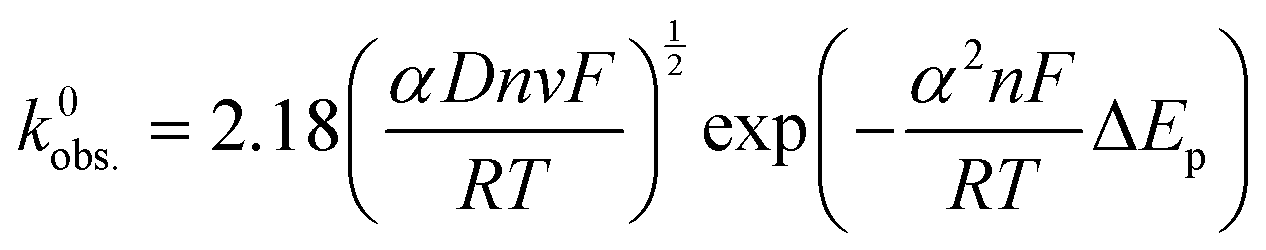
An addition to affecting the measured current, water ingress led to measurable changes in electrode kinetics, which can be inferred from studying the changes in peak-to-peak separation (i.e. ΔEp) between the electrodes, with smaller ΔEp correlating to faster electron transfer. Fig. 4D shows a plot of the ΔEpversus υ for an example electrode of each type, and average values of ΔEp for three electrodes at υ = 50 mV s−1 are given in Table 1. Values of ΔEp can be related to the heterogeneous electron transfer rate, k0obs., using eqn (2) (α is assumed to equal 0.5),27 which is applicable to quasi-reversible electrochemical processes where ΔEp > ∼150 mV.28 Average k0obs. across all scan rates were calculated according to eqn (2), and are listed in Table 1 for comparison.
 | (2) |
It can be seen in Fig. 4D that in both A and NA cases, water ingress appears to cause a decrease in ΔEp, and, subsequently, from eqn (2), an increase in k0obs.. Previous literature using screen-printed electrodes highlighted how increasing electrode resistance causes a decrease in k0obs. due to Ohmic drop,26 but the opposite trend was seen here, with, for example, the NA-I samples showing increased k0obs. compared to the NA-NI samples despite also displaying a large increase in resistance. Furthermore, both A samples show lower k0obs. compared to their comparably immersed NA counterparts, despite their having similar or lower resistances. Therefore, it is concluded that Ohmic drop is not responsible for the observed change in k0obs.. Instead, it is speculated to arise from chemical changes in the electrode, most likely the surface of the carbon black, as this is where electron transfer should take place. However, without more detailed information about the carbon black filler, e.g., its surface functionality and any treatments applied to it before compounding into the FFF filament, it is difficult to reach a definitive conclusion.
4. Conclusions
In conclusion, non-activated and alkali-activated PLA/carbon black composite electrodes were immersed in water for up to 28 days at ambient temperature. This was found to cause no measurable changes in electrode dimensions but did lead to water uptake of approximately 1–1.5% by mass, with activation causing an increased amount and rate of water absorption. In addition, alkali-activation alone was found to cause an uptake of water of approximately 0.2% by mass before immersion. In the case of both activated and non-activated samples, water ingress was found to cause several changes in electrochemical performance as studied by CV using the RuHex redox probe. Firstly, water ingress caused a decrease in the measured peak current, and subsequently an apparent decrease in the electroactive area of the electrode. However, the magnitude of this current decrease appeared to coincide with measured changes in electrode resistance, and so it was concluded to be a consequence of Ohmic drop rather than evidence of a more complex chemical or physical phenomenon. By contrast, the increase in heterogeneous electron transfer rate constant upon immersion appeared independent of electrode resistance and activation.The results of these studies have several implications. Most importantly, they underline the importance of resistance characterisation of electrodes before use to avoid Ohmic drop causing misleading results, as has previously been highlighted for screen printed electrodes.26 Similarly, it can be inferred that long term contact with water should be avoided for AMEs intended to be used for applications where current magnitudes are important, for example in sensing. However, a caveat to this is that in this work whole parts were subjected to immersion rather than the electroactive area alone, as has been the case in previous literature.24 The change in AME resistance would reasonably be expected to scale with the extent of ingress, so water ingress into a relatively small area of a relatively large electrode should cause a relatively lower increase in resistance than ingress into the whole electrode area. Ultimately, therefore, ingress might prove only a minor concern for electrochemists who limit contact of their AME with water to only a small area. Finally, a tangential conclusion of this work is that activation of AMEs with alkali solutions is not suitable for applications requiring dry conditions; for example, such activated AMEs would not be suitable for electrosynthesis in dry solvents without further processing (i.e., drying).
Subsequent work should include establishing more robustly the connection between water ingress and Ohmic drop, and also to establish whether subsequent egress (i.e. drying) of absorbed solvent returns electrodes to their original state. Furthermore, studies should also be carried out to explore the roles of material factors such as polymer type, filler type and surface chemistry, as well as the effects of ingress of different types of solvents and aqueous solutions (e.g., pH, electrolyte concentration, etc.).
Conflicts of interest
There are no conflicts to declare.Acknowledgements
Gary Miller and Hayley Andrews are acknowledged for collection of XPS and SEM data, respectively. Stephen T. Knox is thanked for useful discussions regarding the measurement of solvent ingress into polymers.References
- M. Attaran, The rise of 3-D printing: The advantages of additive manufacturing over traditional manufacturing, Bus. Horiz., 2017, 60(5), 677–688 CrossRef.
- S. C. Ligon, R. Liska, J. Stampfl, M. Gurr and R. Mulhaupt, Polymers for 3D Printing and Customized Additive Manufacturing, Chem. Rev., 2017, 117(15), 10212–10290 CrossRef CAS PubMed.
- O. A. Alimi and R. Meijboom, Current and future trends of additive manufacturing for chemistry applications: a review, J. Mater. Sci., 2021, 56(30), 16824–16850 CrossRef CAS PubMed.
- M. J. Whittingham, R. D. Crapnell, E. J. Rothwell, N. J. Hurst and C. E. Banks, Additive manufacturing for electrochemical labs: An overview and tutorial note on the production of cells, electrodes and accessories, Talanta Open, 2021, 4, 1–8 CrossRef.
- C. Kalinke, N. V. Neumsteir, G. D. Aparecido, T. V. D. Ferraz, P. L. dos Santos, B. C. Janegitz and J. A. Bonacin, Comparison of activation processes for 3D printed PLA-graphene electrodes: electrochemical properties and application for sensing of dopamine, Analyst, 2020, 145(4), 1207–1218 RSC.
- R. M. Cardoso, C. Kalinke, R. G. Rocha, P. L. dos Santos, D. P. Rocha, P. R. Oliveira, B. C. Janegitz, J. A. Bonacin, E. M. Richter and R. A. A. Munoz, Additive-manufactured (3D-printed) electrochemical sensors: A critical review, Anal. Chim. Acta, 2020, 1118, 73–91 CrossRef CAS PubMed.
- A. L. Silva, G. M. D. Salvador, S. V. F. Castro, N. M. F. Carvalho and R. A. A. Munoz, A 3D Printer Guide for the Development and Application of Electrochemical Cells and Devices, Front. Chem., 2021, 9, 19 Search PubMed.
- M. H. Omar, K. A. Razak, M. N. Ab Wahab and H. H. Hamzah, Recent progress of conductive 3D-printed electrodes based upon polymers/carbon nanomaterials using a fused deposition modelling (FDM) method as emerging electrochemical sensing devices, RSC Adv., 2021, 11(27), 16557–16571 RSC.
- A. Ambrosi and A. Bonanni, How 3D printing can boost advances in analytical and bioanalytical chemistry, Microchim. Acta, 2021, 188(8), 17 CrossRef PubMed.
- R. Gusmao, M. P. Browne, Z. Sofer and M. Pumera, The capacitance and electron transfer of 3D-printed graphene electrodes are dramatically influenced by the type of solvent used for pre-treatment, Electrochem. Commun., 2019, 102, 83–88 CrossRef CAS.
- M. Choińska, V. Hrdlička, H. Dejmková, J. Fischer, M. Luděk, E. Vaněčková, V. Kolivoška and T. Navrátil, Applicability of Selected 3D Printing Materials in Electrochemistry, Biosensors, 2022, 12(5), 1–11 CrossRef PubMed.
- U. Sonchaeng, F. Iniguez-Franco, R. Auras, S. Selke, M. Rubino and L. T. Lim, Poly(lactic acid) mass transfer properties, Prog. Polym. Sci., 2018, 86, 85–121 CrossRef CAS.
- V. A. Kefalas, Solvent Crazing as a Stress-Induced Surface-Adsorption and Bulk Plasticization Effect, J. Appl. Polym. Sci., 1995, 58(4), 711–717 CrossRef CAS.
- K. Loos, V. M. Bruere, B. Demmel, Y. Ilmberger, A. Lion and M. Johlitz, Future-Oriented Experimental Characterization of 3D Printed and Conventional Elastomers Based on Their Swelling Behavior, Polymers, 2021, 13(24), 19 CrossRef PubMed.
- D. P. Rocha, R. G. Rocha, S. V. F. Castro, M. A. G. Trindade, R. A. A. Munoz, E. M. Richter and L. Angnes, Posttreatment of 3D-printed surfaces for electrochemical applications: A critical review on proposed protocols, Electrochemical Science Advances, 2021, 1–15 Search PubMed.
- E. M. Richter, D. P. Rocha, R. M. Cardoso, E. M. Keefe, C. W. Foster, R. A. A. Munoz and C. E. Banks, Complete Additively Manufactured (3D-Printed) Electrochemical Sensing Platform, Anal. Chem., 2019, 91(20), 12844–12851 CrossRef CAS PubMed.
- G. Greczynski and L. Hultman, The same chemical state of carbon gives rise to two peaks in X-ray photoelectron spectroscopy, Sci. Rep., 2021, 11(1), 5 CrossRef PubMed.
- R. Blume, D. Rosenthal, J. P. Tessonnier, H. N. Li, A. Knop-Gericke and R. Schlogl, Characterizing Graphitic Carbon with X-ray Photoelectron Spectroscopy: A Step-by-Step Approach, ChemCatChem, 2015, 7(18), 2871–2881 CrossRef CAS.
- T. R. Gengenbach, G. H. Major, M. R. Linford and C. D. Easton, Practical guides for x-ray photoelectron spectroscopy (XPS): Interpreting the carbon 1s spectrum, J. Vac. Sci. Technol., A, 2021, 39(1), 24 CrossRef.
- Institution, T. B. S., Geometrical product specifications (GPS) – Surface texture: Profile. 2022.
- K. Prasad, M. Nikzad, C. M. Doherty and I. Sbarski, Diffusion of low-molecular-weight permeants through semi-crystalline polymers: combining molecular dynamics with semi-empirical models, Polym. Int., 2018, 67(6), 717–725 CrossRef CAS.
- J. P. Guo, C. H. Tsou, Y. Q. Yu, C. S. Wu, X. M. Zhang, Z. J. Chen, T. Yang, F. F. Ge, P. Liu and M. R. De Guzman, Conductivity and mechanical properties of carbon black-reinforced poly(lactic acid) (PLA/CB) composites, Iran. Polym. J., 2021, 30(12), 1251–1262 CrossRef CAS.
- A. Marmur, Soft contact: measurement and interpretation of contact angles, Soft Matter, 2006, 2(1), 12–17 RSC.
- R. D. Crapnell, E. Bernalte, A. Garcia-Miranda Ferrari, M. J. Whittingham, R. J. Williams, N. J. Hurst and C. E. Banks, All-in-One Single-Print Additively Manufactured Electroanalytical Sensing Platforms, ACS Meas. Sci. Au, 2022, 2(2), 167–176 CrossRef CAS.
- A. Garcia-Miranda Ferrari, C. W. Foster, P. J. Kelly, D. A. C. Brownson and C. E. Banks, Determination of the Electrochemical Area of Screen-Printed Electrochemical Sensing Platforms, Biosensors-Basel, 2018, 8(2), 10 Search PubMed.
- M. J. Whittingham, N. J. Hurst, R. D. Crapnell, A. G. M. Ferrari, E. Blanco, T. J. Davies and C. E. Banks, Electrochemical Improvements Can Be Realized via Shortening the Length of Screen-Printed Electrochemical Platforms, Anal. Chem., 2021, 93(49), 16481–16488 CrossRef CAS PubMed.
- R. J. Klingler and J. K. Kochi, Electron-Transfer Kinetics From Cyclic Voltammetry - Quantitative Description Of Electrochemical Reversibility, J. Phys. Chem., 1981, 85(12), 1731–1741 CrossRef CAS.
- M. Velicky, D. F. Bradley, A. J. Cooper, E. W. Hill, I. A. Kinloch, A. Mishchenko, K. S. Novoselov, H. V. Patten, P. S. Toth, A. T. Valota, S. D. Worrall and R. A. W. Dryfe, Electron Transfer Kinetics on Mono- and Multilayer Graphene, ACS Nano, 2014, 8(10), 10089–10100 CrossRef CAS PubMed.
Footnote |
| † Electronic supplementary information (ESI) available. See DOI: https://doi.org/10.1039/d2ma00707j |
| This journal is © The Royal Society of Chemistry 2022 |