DOI:
10.1039/D2MA00646D
(Paper)
Mater. Adv., 2022,
3, 7640-7654
Tuning the nonlinear susceptibility and linear parameters upon annealing Ag60−xSe40Tex nanostructured films for nonlinear and photonic applications†
Received
6th June 2022
, Accepted 3rd August 2022
First published on 3rd August 2022
Abstract
The current study focuses on the annealing-induced changes in the structural, non-linear/linear optical, and surface morphological characteristics of nanostructured Ag60−xSe40Tex (x = 0, 5, 10, and 15%) films. The increase in crystallinity with annealing at 150 °C and 200 °C signifies the structural modifications in films, as observed by XRD and Raman analyses. Lattice shifting with Te doping was also investigated by high-resolution transmission electron microscopy. The changes in the size and surface morphology of particles were verified by field emission scanning electron microscopy. The compositional confirmation and agglomeration of particles in the prepared film were checked via energy-dispersive X-ray spectroscopy. Te doping in the film was also confirmed by X-ray photoelectron spectroscopy. The reduction in the optical bandgap and increase in the Urbach energy of the films upon annealing were calculated from the UV-visible data. The increase in the refractive index with the annealing temperature modified the other linear parameters such as oscillator energy, volume, and surface energy loss function. The skin depth decreased and the extinction coefficient increased with annealing. The increase in the optical density value is good for the film to be used as a solar cell absorbing layer. The increase in the non-linear optical properties, such as the first- and third-order susceptibility, and non-linear refractive index, upon annealing is useful for nonlinear optical and photonic applications.
1. Introduction
Chalcogenide semiconductors have truly been used as multipurpose materials to fabricate various technical devices such as IR detectors, electronic and optical switches, optical recording materials, and optical storage devices.1–5 Although they show numerous unique phenomena, they have the ability to control and change their properties upon exposure to external treatments such as thermal annealing,6 laser irradiation,7 or γ-radiation,8 and swift heavy ion irradiation.9 Thermal annealing induces crystallization in chalcogenide semiconductor materials. The amorphous to crystalline phase transition due to annealing also exhibits large optical absorption changes, enabling the chalcogenide semiconductors to be used in optical storage applications. Due to the technological importance, various studies have been conducted on the effect of annealing on the chalcogenide materials for many optoelectronic devices and other non-linear applications.10–12 Nanostructured thin films are always in demand for their excellent optical and electrical properties with tuneable sizes. The sizes of these nanostructures are highly related to the confinement of charge carriers inside the materials, which play a vital role in the fabrication of optoelectronic devices.13 The thermal annealing effect on Ga11Se77Ag8 chalcogenide thin films shows the amorphous to polycrystalline transformation along with a decrease in the optical bandgap.14 Similarly, the optical properties of Se85Te10Bi5 thin films after the thermal treatment above the glass transition temperature exhibit a phase reversal behaviour.15
Selenium (Se)-based materials are mostly preferred due to their numerous applications such as optical switching and xerography.16 Although pure amorphous Se has a high viscosity, its short lifetime and low stability restrict its applications. To avoid all these difficulties, various other elements such as In, Sb, Sn, Ag, and Bi are alloyed with it.17–21 Among all these additives, silver is one of the most promising elements to be used for potential electronic applications. Silver-containing chalcogenide materials are susceptible to ions and are excellent ionic sensors.22 However, the silver selenide (I–VI) alloy forms a special semiconductor that exhibits enhanced behaviours such as high carrier density, good metal-like properties, and higher mobility of ions.23,24 In this report, the studied materials possess unique nanostructure properties to cause irreversible structural damages and produce higher conductivity for nanomaterials. Moreover, a binary silver selenide is also used as a nanostructured material for various sensing devices due to its low dimensionality. In spite of mild toxicity, silver-containing materials have also been used for solar cell applications and some of biomedicine applications.
Moreover, the binary Ag–Se system is alloyed with other chemical compounds to increase their sensitivity toward the material's electrical, structural, non-linear, and linear optical properties. Ag–In–Se thin films prepared by an electron beam deposition method undergo a drastic change in both optical and structural properties when subjected to thermal annealing at 200 °C and 400 °C.25 Upon intense exposure to light, Ag10Se70Sb10 thin films show a higher photo-conductivity and make them eligible for a sensor device.26 Since tellurium provides rich photosensitivity, a smaller aging effect, and less oxidation in the air, it is considered as a potential element for many chalcogenide thin films. The addition of Te increases the machinability and composite strength of the Ag–Se system.27 Agx(Se80Te20)100−x ultra-thin films prepared via thermal evaporation and annealed below the glass transition temperature (328 K) show structural transformation with an enhanced bandgap upon increase in doping concentrations.28 For some chalcogenide thin films, the annealing effect at various temperatures has showed an increase in conductivity due to the tunnelling of carriers in the localized states.29 Some of the Te-based materials doped with magnetic materials show diverse properties after a thermal treatment.30 For Ge–Fe–Te chalcogenide semiconductor thin films, the annealing process induced a phase transition in their magnetic behaviour by changing their crystal structure and a decrease in the transparency of the film.31 The Sn–Sb–S films annealed at different temperatures have showed higher photoconductivity within a specific range of wavelength.32 In the case of Ga15Se79In6 and Ga15Se81In4 thin films, laser irradiation and thermal annealing revealed amorphous to crystalline phase transition and other significant changes in their optical behaviour for photovoltaic applications.33 Photo-induced changes due to 532 nm laser illumination on Ge12Sb25Se63 amorphous chalcogenide thin films have showed an increase in the bandgap, which supports photobleaching.34 Laser-induced Sb10S40Se50 chalcogenide thin films exhibit a decrease in the optical bandgap, chemical disorder, and enhanced grain size.35 Apart from this, several chalcogenide-based nanostructured materials play a crucial role in light-emitting devices and optoelectronic applications. Many structural changes have been achieved by the heat treatment of nanostructured materials such as 1D Cu2ZnSnS4(CZTS) nanorods get transformed from the nanosphere by the annealing process.36 Similarly, by thermal annealing, CZTS nano-cubes prepared by a sol–gel method changed to nanorods without involving any toxic chemical and high vacuum.37 Ge–Te nanoparticle thin films prepared by the sputtering method possess optical properties in the range of infrared to ultraviolet and also produce phase transition from amorphous to crystalline.38 These phase transition materials are primarily used in numerous optical and random-access memory devices and also have wide applications in computing and photonic devices. Various other kinds of nanomaterials have been grown in the thin-film form to produce different nanostructures such as nanorod heterojunctions, nanosheets, and nanoparticle nano-heterostructures.39,40 The physical properties of (Se70Te30)100–xAgx (0.0 ≤ x ≤ 8.0) ternary glassy alloys show an increase in cohesive energy and average bond strength with a covalency parameter of >90%. The compositions are stable glass formers and may be used in the infrared system.41 The rate of enhancement of transmittance is higher in the infrared regions for Ag2(Se.3Te.7) thin films and quantum confinement and other factors lead to an increase in the band gap, and beyond a specific thickness, the annealing effect becomes dominant and the band gap is continuously lowered.42 From the previous studies, it has been seen that the incorporation of Te into the Ag–Se system alters different linear and non-linear properties of the material for various optical device-related applications.43 The Ag–Se–Te ternary system is an important thermoelectric material system, and typically, it shows the best thermoelectric performance at low temperatures. However, some studies suggest that they can also be used at higher temperatures in the range between 200 and 400 °C.44,45 In this regard, we tried to prepare the nanostructured Ag–Se–Te films by doping Te in the Ag60Se40 binary matrix and induced annealing at temperatures of 150 °C and 200 °C. The Ag–Se–Te system shows good structural, morphological and high non-linear properties. After external energy treatment, it induces various structural, optical as well as morphological changes in it which will enable its future application as an efficient and stable material for many thermoelectric and optoelectronic devices.
The present work investigates the optimization of structural and optical properties of the thermally annealed Ag60−xSe40Tex (x = 0, 5, 10, and 15%) thin films. The crystalline nature of the studied thin film was verified by X-ray diffraction (XRD) and high-resolution transmission electron microscopy (HRTEM), and the corresponding changes in the chemical bonds were confirmed by Raman spectroscopy. Similarly, the compositional and surface morphological alterations were observed using an energy-dispersive X-ray (EDX) spectrometer attached to a field emission scanning microscope (FESEM). The further confirmation of Te doping was done by X-ray photoelectron spectroscopy (XPS). Essential parameters such as linear and non-linear optical properties were calculated from the data taken by UV-Visible spectroscopy using different formulas.
2. Experimental procedure
2.1. Sample preparation
The bulk samples of Ag60−xSe40Tex (x = 0, 5, 10, and 15%) were synthesized by properly mixing highly pure (99.999% Sigma Aldrich) Ag, Se, and Te chemicals via a melt quenching process. A sealed ampoule containing the constituent chemicals was heated at ∼3–4 °C min−1 till 1000 °C inside a furnace and was held for 24 h. The homogeneity of the sample was maintained by the continuous rotation of the ceramic rod inside the furnace using a low-speed motor. The sudden quenching of the heated ampoule was done using ice-cold water. The films of ∼800 nm were prepared from the bulk samples by a thermal evaporation process using a HINDI-HIVAC Model 12A4D coating unit. A cleaned corning glass was used as the substrate, which was first dipped in hydrogen peroxide (H2O2) and further treated with trichloroethylene, acetone, and methanol in an ultrasonic bath. The coating of the film was done at a deposition rate of 0.5 nm s−1 under 10−5 torr vacuum. The prepared films were annealed at 150 °C and 200 °C for 2 h under the pressure of 10−3 torr with a temperature gradient of ∼5 to 6 °C h−1.
2.2. Sample characterization
The structural study of the annealed Ag60−xSe40Tex films was conducted using a Bruker D8 Advanced XRD system with CuKα radiation. The data are taken in the range of 10°–90° at a scan speed of 1° min−1 with a step size of 0.02° s−1 and a grazing angle of 1°. The Raman data were recorded using a LabRAM HR Raman system in the frequency range of 100–400 cm−1 using an argon laser source and a CCD detector in the backscattering mode. The concentration of different elements in the film was checked by EDX, which is attached to the FESEM unit (Carl Zeiss Ultra 55). The surface scanning is done over a 1 × 1 cm2 sample size at 3–4 positions at a 2 × 10⁻⁷ torr vacuum. The Te doping was observed by XPS (Axis Ultra, Kratos Analytical, UK) measurements. The core-level XPS spectra were recorded using Al Kα X-rays (1486.6 eV) with the vacuum of 2 × 10⁻⁹ torr. The scanning was performed at various portions of the sample to reproduce data. The required charge correction has been done with a C 1s binding energy (BE) of 284.6 eV. The calibration factor was used for the correction in the original binding energy (BE) data. The phase identification and inter planar distance of the two annealed Ag60−xSe40Tex thin films were confirmed using a HRTEM (JEM-2100 Plus, Japan). The values were calculated from the HRTEM images obtained using the Image J software. The transmission data of the films were recorded using a Bruker Optics (IFS66v/S UV-Vis spectrometer in the wavelength range 500–1100 nm). Optical quantities such as absorption coefficient, extinction coefficient, bandgap and optical density were determined using different formulas. The refractive index (n), real and dielectric constant (ε1 and ε2) and loss factor were also calculated from the transmission data. The linear parameters were used to evaluate the third-order susceptibility (χ(3)) and nonlinear refractive index (n2).
3. Result analysis and discussions
3.1. Structural study (XRD and Raman spectroscopy)
The XRD graph of Ag60−xSe40Tex annealed films is shown in Fig. 1(a) and various peaks are observed for the studied films. The structural changes confirmed the crystalline nature of the samples after annealing at both the temperatures, i.e. at 150 °C and 200 °C respectively. The peaks observed at 23.46° (110) and 41.02° (211) correspond to the orthorhombic phase of Ag2Se (ICSD Card: 01-071-2410). The peaks observed at 29.03° (101) and 42.37° (012) represent the hexagonal phase of selenium (ICSD card: 01-081-1824), which appeared in all the annealed thin films. The rare peak for a higher tellurium content of the film appeared only at 44.75°, and this revealed a rhombohedral phase of AgTe3 (ICSD Card: 01-076-2328).
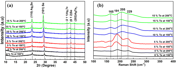 |
| | Fig. 1 (a) XRD graph showing the change in the peak intensity. (b) Temperature-dependent Raman spectra of the annealed Ag60−xSe40Tex films. | |
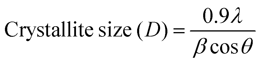
Various structural quantities such as crystalline size, dislocation density, and the number of crystallites per unit surface area are important to get enough information about the structural transformation that occurred in the films. The average crystallite size was calculated from the XRD prominent peaks using the Scherrer's equation:46
| |  | (1) |
where
λ,
θ, and
β are the wavelength, Bragg's angle, and full width at half maximum (FWHM), respectively. The calculated crystallite size was found to be changing upon annealing, as shown in
Table 1. Due to the annealing process, the enhanced grain size increased the crystallite size.
Table 1 Structural quantities of the studied Ag60−xSe40Tex films
| Structural parameters |
0% Te |
5% Te |
10% Te |
15% Te |
| 150 °C |
200 °C |
150 °C |
200 °C |
150 °C |
200 °C |
150 °C |
200 °C |
| Average crystallite size (nm) |
15.23 |
24.51 |
11.10 |
22.99 |
13.38 |
13.31 |
11.69 |
14.04 |
| Dislocation density, δ (nm−2) |
0.0043 |
0.0016 |
0.0081 |
0.0180 |
0.0055 |
0.0056 |
0.0073 |
0.0050 |
|
N
C (nm−2) |
0.0100 |
0.0060 |
0.0110 |
0.0050 |
0.0090 |
0.0092 |
0.0110 |
0.172 |
The dislocation density (δ) and the number of crystallites per unit surface area (Nc) of the films were evaluated as follows:47
| |  | (2) |
where ‘
d’ is the film thickness. The estimated structural quantities for the annealed films are presented in
Table 1. Due to the annealing process, several aggregations occurred and the crystallites per unit area were found to be enhanced with higher annealing.
There is a shift in the XRD pattern of the annealed film, which brings a lattice shift in the crystal. The enlarged view of the (110) plane peak shows the shift of the peak position of the Te-doped films as compared to the undoped Ag60Se40 film. These data are given as supporting document S1 for the manuscript (ESI†). This shift is reflected in the lattice spacing ‘d’ value, which was found from the HRTEM picture.
As stability is one of the important criteria, we performed the structural study (XRD) of the material after keeping it in air for a long period of time. Ironically, the result remains almost the same as before for the 0% Te, 5% Te and 10% Te films. However, there is some change in the intensity of the 15% Te film after aging. Therefore, the material shows almost good stability at ambient temperature also. This confirms the material's applicability in various optoelectronic fields for a long time. We present the comparative XRD pattern of the previous and present observation (AG-after aging) to show the stability of the materials as supporting document (S2, ESI†).
Structural information such as chemical bonds and atomic arrangements are the key entities to get a detailed view of the studied samples. Raman spectroscopy is an essential experimental technique for the study of different vibrational modes in films. The spectral investigation of annealed films is shown in Fig. 1(b). The 229 cm−1 peak in the graph might be due to the existing trigonal Se crystallites for selenium.48 This peak intensity reduced with the increase in the annealing temperature for a higher Te dopant in the Ag–Se–Te system. The obtained peak at 165 cm−1 refers to Te–Te homopolar bonds and its intensity increased with the annealing temperature.49 Similarly, the peak found at 205 cm−1 might be the signal of the Ag–Se vibrational mode.50
3.2. Morphological and compositional study (EDX, XPS, FESEM and TEM)
The presence of different chemical elements with percentage is noticed from the peaks seen in the EDX, as shown in Fig. 2(a and b) insets. The elemental composition was found to be within 3% variation from the pristine composition, as shown in Table 2. FESEM is an essential tool for analyzing the grain size, surface morphology, etc., for various thin films. Fig. 2(a and b) illustrate the shape and variations of the particles due to the annealing process for various compositions. There is no such change in grain or particle size for the Ag–Se host matrix by annealing at higher temperatures. They almost exhibit similar particle sizes with small variations. With the increase in the Te concentration, there is a drastic change in the shape and size of particles after annealing. The FESEM pictures of Ag55Se40Te5 thin films showed nano-rod-like particles, and their size increased with the annealing temperature.
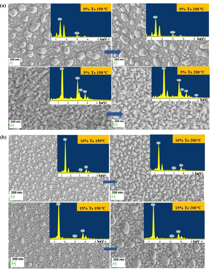 |
| | Fig. 2 (a) FESEM image and the EDX picture of Ag60Se40 and Ag55Se40Te5 thin films annealed at 150 °C and 200 °C. (b) FESEM images and EDX (inset) pictures of Ag50Se40Te10 and Ag45Se40Te15 films annealed at 150 °C and 200 °C. | |
Table 2 Composition of different Ag60−xSe40Tex (x = 0, 5, 10, and 15 at%) annealed thin films at 150 °C and 200 °C temperatures
| Sample |
Ag60Se40 |
Ag55Se40Te5 |
Ag50Se40Te10 |
Ag45Se40Te15 |
| Temp. |
|
150 °C |
200 °C |
|
150 °C |
200 °C |
|
150 °C |
200 °C |
|
150 °C |
200 °C |
| Element |
Cal (at%) |
Obs (at%) |
Obs (at%) |
Cal (at%) |
Obs (at%) |
Obs (at%) |
Cal (at%) |
Obs (at%) |
Obs (at%) |
Cal (at%) |
Obs (at%) |
Obs (at%) |
| Ag |
60 |
57.95 |
57.85 |
55 |
52.86 |
52.55 |
50 |
49.13 |
49.16 |
45 |
44.68 |
44.58 |
| Se |
40 |
42.05 |
42.15 |
40 |
42.52 |
42.70 |
40 |
41.25 |
41.07 |
40 |
41.12 |
41.10 |
| Te |
0 |
0 |
0 |
05 |
04.62 |
04.75 |
10 |
09.62 |
09.77 |
15 |
14.20 |
14.32 |
| Total |
100 |
100 |
100 |
100 |
100 |
100 |
100 |
100 |
100 |
100 |
100 |
100 |
Similarly, the grain size of the Ag50Se40Te10 thin film increased as compared to the Ag55Se40Te5 thin film. However, a 10% Te thin film at 150 °C exhibits an increased particle size than the thin film annealed at 200 °C. For the higher Te content, i.e., Ag45Se40Te15 thin film, the particle size increased at 200 °C. This growth in the grain size and disappearance of small grains after annealing show a decrease in the disorders with high tellurium concentrations.51Fig. 3 shows the particle size histogram of the films annealed at 150 °C and 200 °C.
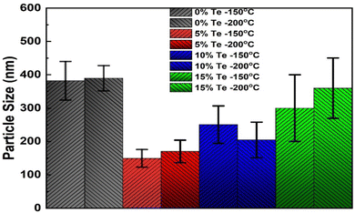 |
| | Fig. 3 Particle size distribution histogram of films. | |
XPS analysis
The Te 4d peak is absent in the 0% Te (Ag60Se40) 200 °C annealed film, whereas the Te 4d peak is clearly observed at 40.4 eV for the 15% Te (Ag45Se40Te15) 200 °C annealed film (Fig. 4). This indicates Te doping in the Ag60−xSe40Tex film. The Se 3d peak at 54.91 eV and Ag 4p peak at 63 eV are present in both the 0% Te and 15% Te 200 °C annealed films, respectively. There is a small peak shift along with the decrease in the intensity of these two peaks with Te doping. The decrease in the intensity of Se 3d and Ag 4p peaks is due to the development of the Te 4d peak.
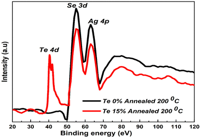 |
| | Fig. 4 XPS core level spectra of (a) Ag60Se40 and (b) Ag45Se40Te15 thin films annealed at 200 °C. | |
TEM analysis
The phase identification and inter planner distance of the two annealed Ag60−xSe40Tex thin films were confirmed by high-resolution transmission electron microscopy (HRTEM) (JEM-2100 Plus, Japan). The values were calculated from the HRTEM images obtained using the Image J software. Transmission electron microscopy is one of the important tools for calculating the structural and morphological parameters of the material under study. Fig. 5(a and b) represent the HRTEM images of the 200 °C annealed Ag60Se40 and Ag45Se40Te15 thin films, respectively. Both the figures show the Ag2Se phase with hkl value (110) of the studied film. For the 0% Te film, the d value is 3.681 Å, which changed to 3.695 Å for the 15% Te film. Such change of 0.014 Å in the d value is due to the lattice shifting in the crystal, which is in good agreement with the XRD pattern obtained from the structural analysis. This shifting is due to the annealing at higher temperatures, which causes an increase in crystallinity also.
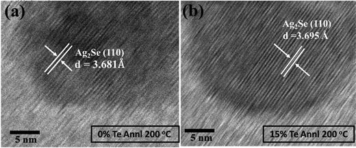 |
| | Fig. 5 HRTEM images of (a) Ag60Se40 and (b) Ag45Se40Te15 thin films annealed at 200 °C. | |
3.3. Optical property study
3.3.1. Transmission (T) and absorption coefficient (α) analysis.
The transmittance spectra of the annealed Ag60−xSe40Tex (x = 0, 5, 10, and 15 at%) films in the wavelength range of 500–1100 nm are shown in Fig. 6a. The transmittance value is reduced with the increase in Te content for higher annealing temperatures. The reduction in T% with annealing is due to the crystallization of the film structure by increasing the crystallite size with annealing, as observed from the XRD study. It is also observed that the absorption edge moves towards higher λ (redshift), i.e. to a lower energy region. The absorbing ability of the material is defined as the absorption coefficient (α). The amount of radiation absorbed by the material from the incident electromagnetic radiation is a function of the film thickness and the incident energy (hν), which is related as follows:52| |  | (3) |
where ‘d’ is the film thickness. Fig. 6b represents the plot between α and λ, and the obtained α value is of the order of 104 cm−1. It illustrates that the α value decreased with the annealing temperature. This decrease in the α value for the studied samples indicates the higher growth of crystallites due to annealing. Some of the chalcogenide materials also possess higher absorbance in the order of 104 cm−1 and are also used as brilliant materials for solar cell applications.
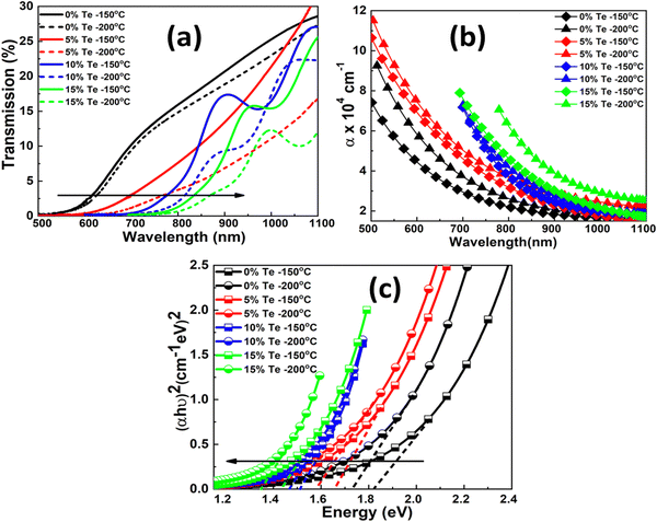 |
| | Fig. 6 (a) Transmission spectra of the annealed Ag60−xSe40Tex films. (b) Change of α with λ for different annealed films. (c) Evaluation of direct bandgap of the studied annealed films. | |
3.3.2. Optical bandgap (Eg), Tauc's parameter (B2) and Urbach energy (Eu).
Bandgap plays a very significant role for semiconducting material in deciding various optoelectronic applications. The energy gap value was calculated from α and the incident photon energy (hν) in the strong absorption region (α ≥ 104 cm−1), which is known as Tauc's formula:53where Eg, B and p are the optical bandgap, Tauc parameter and exponent factor respectively. The Tauc parameter depends on the transition probability, whereas the p value decides the type of electronic transition. Depending on the transition mode, ‘p’ has different values such as p = 1/2 (direct allowed), 2 (indirect allowed), 3/2 (direct forbidden) and 3 (indirect forbidden) transitions.
The accurate fit of the experimental results for p = 1/2 of the annealed Ag–Se–Te films using eqn (4), i.e., the change in (αhν)2 with hν is shown in Fig. 6c. This indicates that the direct allowed transition occurred in the films. The slope from the linear fitting of (αhν)2 and hν plot gives the Tauc parameter and the intercept gives the optical bandgap energy. The calculated bandgap value for the annealed films reduced with the increase in annealing temperature, which is shown in Table 3. This reduction in the bandgap values is due to the structural transformation by annealing. Similar kinds of behaviors were observed by many researchers.54,55 The Tauc parameter for the Ag60Se40 host matrix increased with the annealing temperature. However, the other thin films exhibit the opposite behavior as shown in Table 3.
Table 3 Calculated optical parameters of annealed Ag60−xSe40Tex thin films
| Optical parameters |
0% Te |
5% Te |
10% Te |
15% Te |
| 150 °C |
200 °C |
150 °C |
200 °C |
150 °C |
200 °C |
150 °C |
200 °C |
| Optical bandgap (Eg) eV |
1.82 ± 0.01 |
1.73 ± 0.02 |
1.66 ± 0.01 |
1.59 ± 0.01 |
1.51 ± 0.02 |
1.46 ± 0.01 |
1.43 ± 0.01 |
1.34 ± 0.02 |
| Tauc parameter (B2) cm−2 eV−2 (B2 × 1010 esu) |
6.32 |
7.13 |
7.95 |
6.85 |
7.38 |
6.21 |
5.88 |
4.24 |
| Urbach energy (eV) |
0.734 |
0.644 |
0.648 |
0.695 |
0.383 |
0.398 |
0.410 |
0.612 |
| Dispersion energy, Ed (eV) |
0.32 |
0.36 |
0.29 |
0.31 |
0.25 |
0.20 |
0.22 |
0.24 |
| Oscillator energy, E0 (eV) |
2.15 |
2.13 |
1.93 |
1.79 |
1.69 |
1.60 |
1.57 |
1.52 |
| First moments of optical spectra (M−1) |
0.149 |
0.170 |
0.151 |
0.173 |
0.152 |
0.124 |
0.141 |
0.162 |
| Second moments of optical spectra (M−3) |
0.032 |
0.037 |
0.040 |
0.054 |
0.052 |
0.048 |
0.057 |
0.070 |
| Static refractive index (n0) |
1.0722 |
1.0820 |
1.0729 |
1.0831 |
1.0735 |
1.0798 |
1.0812 |
1.0854 |
| Oscillator strength f (EdE0) |
0.696 |
0.777 |
0.564 |
0.555 |
0.439 |
0.322 |
0.349 |
0.376 |
| Static linear dielectric constant (ε∞) |
1.148 |
1.170 |
1.151 |
1.173 |
1.152 |
1.124 |
1.141 |
1.162 |
| High-frequency dielectric constant (εL) |
1.04 |
1.66 |
1.75 |
2.14 |
1.67 |
2.10 |
3.29 |
3.16 |
| Carrier concentration (N/m*) × 1039 kg−1 m−3 |
2.16 |
3.69 |
2.87 |
2.83 |
2.57 |
3.02 |
4.66 |
3.95 |
| Non-linear refractive index (n2 × 10−16 esu) |
1.198 |
2.025 |
1.237 |
2.083 |
1.279 |
1.801 |
1.910 |
2.331 |
| First-order nonlinear optical susceptibility, χ(1) in esu |
0.0119 |
0.0136 |
0.0120 |
0.0137 |
0.0121 |
0.0132 |
0.0134 |
0.0141 |
| Third-order non-linear susceptibility (χ(3) × 10−18 esu) |
3.409 |
5.815 |
3.525 |
5.988 |
3.644 |
5.161 |
5.481 |
6.719 |
| Optical electronegativity (ηOpt) |
2.2091 |
2.2041 |
2.2088 |
2.2035 |
2.2085 |
2.2053 |
2.2045 |
2.2024 |
| Plasma frequency (ωp × 106) Hz |
2.44 |
2.53 |
2.17 |
1.95 |
2.10 |
2.03 |
2.02 |
1.89 |
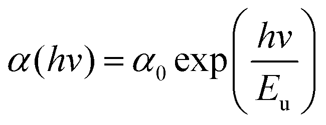
However, the absorption mechanism in the weakly absorbing region (α < 104 cm−1) is governed by the exponential relation known as the Urbach's rule. The absorption of photons between the localized states and extended band states depends on the Urbach energy. The exponential Urbach relation is expressed as follows:56
| |  | (5) |
where
Eu and
α0 are the Urbach energy and a constant respectively. The
Eu value was obtained from the reciprocal of the slope of the straight-line fitting of ln(
α/
α0)
vs. energy (
hν). The evaluated ‘
Eu’ value is presented in
Table 3, which shows an increasing nature with the temperature. Due to the heat treatment, crystallites broke down into smaller size crystals, which results in an increase in the surface dangling bonds in the thin films. The concentration of localized states increased with the increase in the surface dangling bonds for which the localized states widened.
28,57 Such widening of localized states decreased the bandgap of the film.
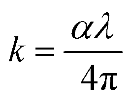
3.3.3. Extinction coefficient (k), skin depth (δ) and optical density (OD).
The absorbing power of the film is also expressed by extinction coefficient (k), which is due to the interaction of the incident electromagnetic wave with the material. The value was estimated from the α value by,58 . The variation between ‘k’ and ‘hν’ is given in Fig. 7a, which infers the increase in k with annealing at high temperatures. It confirms the higher absorption power of the sample and its potential use in many optoelectronics storage devices. A similar behavior has also been seen in nanostructured SnS thin films, where SnS thin films were deposited by varying the substrate temperatures. Due to this increasing behavior of extinction coefficients, these nanostructure materials are also used in photo-detection devices.59
 |
| | Fig. 7 (a) k vs. hν plot for the annealed Ag60−xSe40Tex films. (b) Optical density vs. wavelength for annealed Ag60−xSe40Tex thin films. (c) Plot between δ vs. hν for the annealed Ag60−xSe40Tex films. (d) Change in n with λ for the annealed films. | |
Similarly, the optical density (OD) is a necessary linear parameter, which is related to the change in α and is expressed as OD = α × d, where ‘d’ is the film thickness. The plot between the OD and λ is presented in Fig. 7b, which shows the decreased value of OD with the increased annealing temperature. Skin depth (δ) is defined as the reciprocal of ‘α’ and attributes to many optical properties, the density of the film, and other microstructure of the films. The skin depth was evaluated as δ = 1/α, and the skin depth was found to be more with annealing, as shown in Fig. 7c.
3.3.4. Linear refractive index (n), oscillator and dispersion energy ((E0, Ed)).
The refractive index (n) describes the spectral distribution of the material at different wavelengths from which many essential linear and non-linear parameters are evaluated by using the value of ‘n’. The ‘n’ value of the material is being evaluated by using the following relation:60| |  | (6) |
where ‘T’ is the transmission percentage. The ‘n’ vs. wavelength graph is given in Fig. 7d, that shows the increase in refractive index with the annealing temperature. This is also observed in many nanostructured thin films, which made them potential candidates for the application of various photonic and non-linear applications.
The single effective model (SEO) was used to evaluate the dispersion energy and oscillator energy (Ed and E0) by using the optical data. The static refractive index (n0), dielectric constants, the moments M−1 and M−3, etc., were evaluated from these two parameters. The dispersion relation using these parameters is expressed as follows:61
which is rewritten as
| |  | (7) |
These energies give enough knowledge about the material's overall band structure, which is required for various applications in the optoelectronic field. The
E0 and
Ed values were calculated from the slope

and intercept

values of the plot between (
n2 − 1)
−1 and (
hν)
2, as shown in
Fig. 8a. The estimated values are listed in
Table 3, which shows the decrease in
E0 with the annealing temperature, whereas the
Ed value increased with the annealing temperature except for the Ag
50Se
40Te
10 thin film.
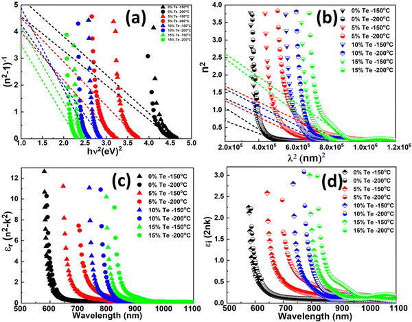 |
| | Fig. 8 (a) E0 and Ed evaluation. (b) Calculation of N/m* and ε∞. (c) Real dielectric constant (εr). (d) Imaginary dielectric constant (εi) with wavelength plot of Ag60−xSe40Tex films. | |
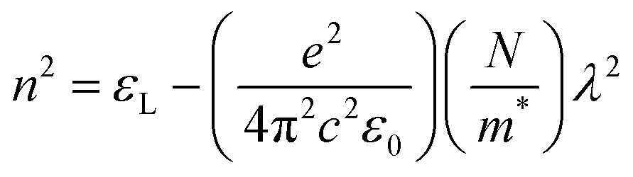
Based on the SEO model, the zero-frequency dielectric constant (ε∞) and the static refractive index (n0) of the annealed thin film were calculated using the equations:62
| |  | (8) |
The
ε∞ value decreased and the
n0 value increased with the annealing temperature, which are given in
Table 3. The oscillator strength is one the important parameters obtained from the WDD model and is calculated by taking the product of
E0 and
Ed,
i.e. f =
E0Ed. The obtained ‘
f’ value is given in
Table 3, and it is seen that its value increased for the Ag
60Se
40 and Ag
45Se
40Te
15 thin films, whereas the value for other two films decreased with annealing.
The first-order (M−1) and third-order optical moments (M−3) were determined from the dispersive energy values of the annealed thin films:63
On rearranging the above-mentioned equations,
| |  | (9) |
The obtained values of
M−1 and
M−3 are shown in
Table 3 and both the values increased with the increase in the annealing temperature. However, for the 10% Te thin film, they behave exactly in the opposite way,
i.e. decreased with the annealing temperature.
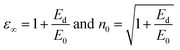
3.3.5. High-frequency dielectric constant (εL), carrier concentration (N/m*) and plasma frequency (ωp).
The dielectric constant is a dynamic parameter of the material, which is used for different practical applications. The high-frequency dielectric constant (εL) was obtained using the following equation:64| | 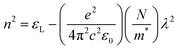 | (10) |
The plot between n2vs. λ2 is shown in Fig. 8b and was used to evaluate the value of N/m* and εL which are listed in Table 3. The  and εL increased with the increase in annealing. The N/m* depends on the internal microstructure of the films. With annealing, the crystallinity increased for which the N/m* value increased with annealing.
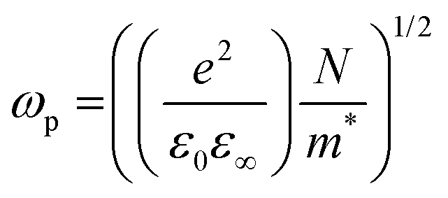
According to Drude's theory, the carrier concentration  of the material is related to the plasma frequency (ωp) using the following expression:65
which is rearranged to
| | 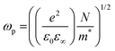 | (11) |
For the Ag
60Se
40 thin film, the
ωp value exhibits an increased value with the annealing temperature but for the rest of all it decreased with a higher annealing temperature.
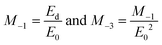
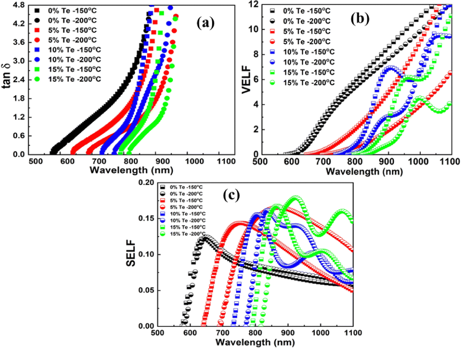
3.3.6. Complex dielectric constant, loss factor, volume and surface energy loss function and optical electronegativity (ηOpt).
For electrical applications of the semiconducting materials, many parameters directly depend on the dielectric properties, and to a large extent, it also depends on the electronic properties of the material. The dielectric property depends on the bandgap which is modified by the electromagnetic radiation through the film. The dielectric properties of the material are linked with dissipation energy and storage. The complex dielectric is defined as66ε = ε1 + iε2, where ε1 = n2 − k2 and ε2 = 2nk are the real and imaginary parts respectively. The term ε1 is related to the dispersion of the electromagnetic wave propagation within the film and causes for the damping of the electromagnetic wave through materials. However, ε2 is associated with the energy absorption from electric field due to the dipole motion and provides necessary information regarding the disruptive rate of the wave inside the material. The variation in ε1 and ε2 with wavelength is shown in Fig. 8c and d, respectively.
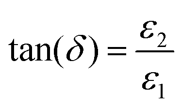
The ratio of ε2 to ε1, i.e., the loss factor was estimated from the relation67 .
.
The power loss due to an oscillation of dipoles in a dissipative medium is also known as the dissipation factor (tan![[thin space (1/6-em)]](https://www.rsc.org/images/entities/char_2009.gif) δ). Fig. 9(a) represents the variation between the loss factor and the incident photon energy. The tangent loss exhibits an increasing nature with the wavelength for the increased Te concentration.
δ). Fig. 9(a) represents the variation between the loss factor and the incident photon energy. The tangent loss exhibits an increasing nature with the wavelength for the increased Te concentration.
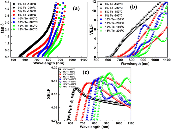 |
| | Fig. 9 (a) Loss factor with the wavelength and the change in (b) VELF and (c) SELF for annealed Te-doped Ag60−xSe40Tex thin films. | |
The VELF and SELF are directly related to ε1 and ε2 as follows:68
| |  | (12) |
The VELF and SELF values of the films were calculated, and the plot between the energy loss functions and wavelength is presented in
Fig. 9b and c.
The ability of the positive radicals of atoms of any material to attract the electrons to form the ionic bonds is called optical electronegativity (ηOpt). It can be estimated for any solid material using the equation69
| |  | (13) |
where
C = 25.54, which is a constant. The obtained value of optical negativity is tabulated in
Table 3, and it exhibits a decreasing nature with the increase in the annealing temperature.
3.4 Nonlinear optical study
3.4.1. First (χ(1)) and third (χ(3))-order nonlinear susceptibility.
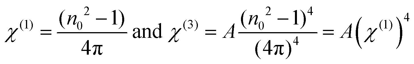
When the material is reacted with the non-linear medium, the polarization no longer behaves linearly with the associated electric field. The non-linearity plays and responds differently with varying electric fields. The high-intense electric field modifies the non-linear parameters upon falling on the films. Various material-dependent entities such as bond length, electronic polarizability, and nuclear interaction are dependent on the non-linear properties in chalcogenide films. The first non-linear susceptibility and third-order non-linearity were evaluated using the Miller's formula:70,71| |  | (14) |
where ‘n0’ is the static refractive index at hν → 0 and A = 1.7 × 10⁻¹⁰ esu. It is observed that the third-order non-linear susceptibility increased with annealing at higher temperatures and also it is more with a higher Te content. A similar behavior is also seen in some reports, where the non-linear susceptibilities exhibit an enhanced behavior with the increase in the annealing temperature.65,72,73 Non-linear susceptibilities are mainly due to the pure electronic effects of the material and most transparent materials provide non-linearity from anharmonic terms of the polarization of bound electrons. For many chalcogenides, the non-linear susceptibility value is in higher order than that of several oxide glasses. Meanwhile, due to the non-resonant third-order susceptibilities of chalcogenide materials, these are considered promising elements for optical switching and other related applications.74 Further by increasing the annealing temperature, there is also increase in crystal defects, resulting in higher polarization. Additionally, lone pair electrons also contribute to enhancing polarization and made the chalcogenide material promising for potential use in various optical device applications.47 As tellurium possesses a larger radius than that of sulfur and selenium, it exhibits a higher polarizability than the other two. This leads to an increase in non-linear susceptibilities with the increase in the tellurium content.
Chalcogenide materials are the adopted candidates for middle and infrared second-order non-linear optical materials. Several chalcogenide based materials are used to produce large optical nonlinearity with good efficiency.75 Other halogen-rich chalcogen materials show pronounced non-linear optical behaviors due to their chiral property.76 These materials are also used for the infrared nonlinear optical applications and mostly produce high-performance nonlinear optics. The Sn10Br10S2 chalcohalide material exhibits a phase-matchable behavior with various particle sizes with a bandgap around 2.56 eV. Annealed In15Sb10S15Se60 thin films show a higher value of non-linear susceptibilities than the studied films and might be used for photonic applications.77 The obtained value of the studied annealed Ag–Se–Te thin films shows non-linear susceptibilities in a greater order, hence proving its applicability in various optoelectronic fields.
3.4.2. Nonlinear refractive index (n2).
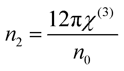
As non-linearity is one of the important parameters for many potential optical applications, the value of the nonlinear refractive index plays a vital role in it. Depending upon the value, it can be considered for efficient use in the optoelectronic field such as capacity communication systems and optical glass fibers.78 Moreover, depending upon the empirical relation of the Miller rule,79 the non-linear index of refraction (n2) was calculated from the static refractive index (n0) by the relation  . The calculated n2 values are listed in Table 3. It was found that the non-linear refractive index of the studied films decreased with the doping content. However, its magnitude increased with the annealing temperature.
Non-linear refractive index signifies the concept of self-refraction. The glasses having a n2 value greater than zero exhibit a particular behaviour, where the beams propagating through the material show periodic self-focusing rather than diffracting the beam in the glass.80 Another study of thermally annealed TlInS2 nanostructured thin films reports a higher value of the non-linear refractive index of order 10−10 esu and exhibits an increased pattern with thermal treatments.81
4. Conclusion
The present report infers increase in the crystalline nature in Ag60−xSe40Tex films by annealing at 150 °C and 200 °C. The XRD study revealed the structural transition with the increase in crystallite size and the decrease in the dislocation density of the films with Te% and annealing temperature. The decrease in transmittance and increase in the optical absorption coefficient with annealing temperature is observed from the UV-visible data. The significant increase in the refractive index brings more freedom in designing multifunctional nonlinear optical devices. The change in the direct optical bandgap is explained on the basis of density of defect states and degree of disorder. The skin depth decreased and the extinction coefficient increased with annealing. The plasma frequency decreased due to the increase in the carrier concentration. The increase in the optical density value is good for the film to be used as the solar cell absorbing layer. The annealing temperature also significantly influences the oscillator energy, VELF and SELF. The χ(3), n2 value increased with annealing, whereas the optical electronegativity decreased. The plasma frequency decreased due to the increase in the carrier concentration. The change in these linear and nonlinear parameters is useful for nonlinear optical device applications. The enhanced value of non-linear parameters is also a consequence of the structural modification induced by the thermal annealing process. Meanwhile, by using different bandgap materials, various nanostructures can be made to form nanojunctions, which are mostly used for different sensor devices. Due to the low dimensionality of chalcogenide materials, such kind of ternary nanostructures are also used for different thermoelectric applications and the presence of silver made them more valuable candidates for electrical applications.
Data availability statement
The data that support the findings of this study are available from the corresponding author upon reasonable request.
Conflicts of interest
There are no conflicts to declare.
Acknowledgements
R. Naik thanks Indian Institute of Science for FESEM, Optical, and Raman measurements. Also Dr Naik thanks ICT-IOC for Start-up grant.
References
- H. Li and J. Robertson, Materials selection and mechanism of non-linear conduction in chalcogenide selector devices, Sci. Rep., 2019, 1867, 1–9 Search PubMed.
- T. Cao and M. Cen, Fundamentals and applications of chalcogenide phase-change material photonics, Adv. Theory Simul., 2019, 2, 1900094–1900111 CrossRef.
- B. J. Eggleton, B. Luther-Davies and K. Richardson, Chalcogenide photonics, Nat. Photonics, 2011, 5, 141–148 CrossRef CAS.
- M. M. Rahman, K. Rukmani and S. Asokan, Electrical switching studies on Ge–Te–Tl chalcogenide glasses: Effect of thallium on the composition dependence of switching voltages, J. Non-Cryst. Solids, 2011, 357, 946–950 CrossRef CAS.
- S. Hudgens, Progress in understanding the Ovshinsky Effect: Threshold switching in chalcogenide amorphous semiconductors, Phys. Status Solidi B, 2012, 249, 1951–1955 CrossRef CAS.
- D. Sahoo, P. Priyadarshini, A. Aparimita, D. Alagarasan, R. Ganesan, S. Varadharajaperumal and R. Naik, Role of annealing temperature on optimizing the linear and nonlinear optical properties of As40Se50Ge10 films, RSC Adv., 2020, 10, 26675–26685 RSC.
- P. Pradhan, R. Naik, N. Das and A. K. Panda, Band gap tuning in As40Se53Sb07 thin films by 532 nm laser irradiation: An optical investigation by spectroscopic techniques, Opt. Mater., 2018, 75, 699–709 CrossRef CAS.
- M. S. Ailavajhala, Y. Gonzalez-Velo, C. Poweleit, H. Barnaby, M. N. Kozicki, K. Holbert, D. P. Butt and M. Mitkova, Gamma radiation induced effects in floppy and rigid Ge-containing chalcogenide thin films, J. Appl. Phys., 2014, 115, 043502 CrossRef.
- M. Behera, N. C. Mishra, S. A. Khan and R. Naik, Influence of 120 MeV Ag Swift Heavy Ion Irradiation on the optical and electronic properties of As-Se-Bi chalcogenide thin films, J. Non-Cryst. Solids, 2020, 544, 120191 CrossRef CAS.
- S. A. Khan, M. Zulfequar and M. Husain, Effects of annealing on crystallization process in amorphous Ge5Se95-xTex thin films, Phys. B, 2002, 324, 336–343 CrossRef CAS.
- O. El-Shazly and M. M. Hafiz, Annealing effects on the structural and optical characteristics of electron beam deposited Ge-Se-Bi thin films, J. Mater. Sci.: Mater. Electron., 2001, 12, 395–401 CrossRef CAS.
- M. A. Alvi, Influence of thermal annealing on optical constants of Ag doped Ga–Se chalcogenide thin films, Opt. Commun., 2013, 295, 21–25 CrossRef CAS.
- T. Xu, Y. Shen, K. Yin and L. Sun, Precisely monitoring and tailoring 2D nanostructures at the atomic scale, APL Mater., 2019, 7, 050901 CrossRef.
- H. E. Atyia and A. S. Farid, The Effect of annealing above glass transition temperature on the optical properties of Se85Te10Bi5 thin film, J. Electron. Mater., 2016, 45, 357–364 CrossRef CAS.
- T. V. Moreno, L. C. Malacarne, M. L. Baesso, W. Qu, E. Dy, Z. Xieb, J. Fahlman, J. Shen and N. G. C. Astrath, Potentiometric sensors with chalcogenide glasses as sensitive membranes: a short review, J. Non-Cryst. Solids, 2018, 495, 8–18 CrossRef CAS.
- A. R. Barik, K. V. Adarsh, R. Naik, R. Ganesan, G. D. Yang, H. Jain and K. Shimakawa, Role of rigidity and temperature in the kinetics of photodarkening in GexAs(45-x)Se55 thin films, Opt. Exp., 2011, 19, 13158–13163 CrossRef CAS PubMed.
- R. Panda, R. Naik and N. C. Mishra, Thermal annealing induced evolution of AgIn5Se8 phase from Ag/In2Se3 bilayer thin film, J. Alloys Compd., 2019, 778, 819–826 CrossRef CAS.
- R. Naik, A. Jain, R. Ganesan and K. S. Sangunni, Compositional dependence optical properties study of As40Se60−xSbx thin films, Thin Solid Films, 2012, 520, 2510–2513 CrossRef CAS.
- Y. Huang, F. Chen, B. Qiao, S. Dai, Q. Nie and X. Zhang, Improved nonlinear optical properties of chalcogenide glasses in Ge-Sn-Se ternary system by thermal treatment, Opt. Mater. Exp., 2016, 6, 1644–1652 CrossRef CAS.
- M. Frumar and T. Wagner, Ag doped chalcogenide glasses and their applications, Curr. Opin. Solid State Mater. Sci., 2003, 7, 117–126 CrossRef CAS.
- A. Aparimita, M. Behera, C. Sripan, R. Ganesan, S. Jena and R. Naik, Effect of Bi addition on the optical properties of Ge30Se70-xBix thin films, J. Alloys Compd., 2018, 739, 997 CrossRef CAS.
- A. Z. Mahmoud, M. A. Abdel-Rahim and M. Mohamed, Role of the annealing temperature for optimizing the optical and electronic parameters of Ge10Se75Ag15 films for optoelectronic applications, Opt. Quantum Electron., 2021, 53, 236 CrossRef CAS.
- Y. Cao, X. Zhu, H. Chen, X. Zhang, J. Zhou, Z. Hu and J. Pang, Towards high efficiency inverted Sb2Se3 thin film solar cells, Sol. Energy Mater. Solar Cells, 2019, 200, 109945 CrossRef CAS.
- V. Sasikala and K. Chitra, All optical switching and associated technologies: A review, J. Opt., 2018, 47, 307–317 CrossRef.
- T. Colakoglu and M. Parlak, Structural characterization of polycrystalline Ag-In-Se thin films by e-beam technique, Appl. Surf. Sci., 2008, 254, 1569–1577 CrossRef CAS.
- K. S. Bindra, N. Puri and R. Thangaraj, Transient photoconductivity in amorphous Se70Sb20Ag10 thin films, J. Non-Cryst. Solids, 2007, 353, 1446–1449 CrossRef CAS.
- M. Mishra, R. Chauhan and K. K. Srivastava, The effect of annealing on some optical properties in Se-Te-Ag glasses, Integr. Ferroelectr., 2010, 118, 34–44 CrossRef CAS.
- D. Singh, S. Kumar and R. Thangaraj, Optical and electrical properties of as-prepared and annealed (Se80Te20)100–xAgx (0 ≤ x ≤ 4) ultra-thin film, J. Non-Cryst. Solids, 2012, 358, 2826–2834 CrossRef CAS.
- S. Jindal, S. Singh, G. S. S. Saini and S. K. Tripathi, Optimization of thermoelectric powder factor of (013)- oriented Ag2Se films via thermal annealing, Mater. Res. Bull., 2021, 145, 111525 CrossRef.
- J. Liu, S. Daning and H. Yang, Heat-treatment-induced compositional evolution and magnetic state transition in magnetic chalcogenide semiconductor GeFeTe without structural phase change, ACS Appl. Mater. Interfaces, 2017, 9, 38651–38661 CrossRef CAS.
- F. S. Al-Hazmi, Effect of annealing on optical constants of Se75S25-xCdx chalcogenide thin films, Phys. B: Condens. Matter, 2009, 404, 1354–1358 CrossRef CAS.
- N. Ali, S. T. Hussain, Y. Khan, N. Ahmad, M. A. Iqbal and S. M. Abbas, Effect of air annealing on the band gap and optical properties of SnSb2S4 thin films for solar cell application, Mater. Lett., 2003, 100, 148–151 CrossRef.
- A. A. Al-Ghamdi, S. A. Khan, S. Al-Heniti, F. A. Al-Agel, T. Al-Harbi and M. Zulfequar, Effects of laser irradiation on optical properties of amorphous and annealed Ga15Se81In4 and Ga15Se79In6 chalcogenide thin film, J. Alloys Compd., 2010, 50, 229–234 CrossRef.
- R. Naik, S. Jena, R. Ganesan and N. K. Sahoo, Effect of laser irradiation on optical properties of Ge12Sb25Se63 amorphous chalcogenide thin films, Ind. J. Phys., 2015, 89, 1031–1040 CrossRef CAS.
- R. Naik, S. Jena, R. Ganesan and N. K. Sahoo, Laser-induced optical properties changes in Sb10S40Se50 chalcogenide thin films: an investigation through FTIR and XPS measurement, Phy. Status Solidi B, 2014, 251, 661–668 CrossRef CAS.
- G. Rajesh, N. Muthukumarasamy, D. Velauthapillai and S. K. Batabyal, Annealing induced shape transformation of CZTS nanorods based thin films, Langmuir, 2017, 33, 6151–6158 CrossRef CAS PubMed.
- G. Rajesh, N. Muthukumarasamy, S. Agilan, D. Velauthapillai, K. Mohanta and S. K. Batabyal, Electrical bistability of sol-gel derived Cu2ZnSnS4 thin films, Mater. Lett., 2018, 220, 285–288 CrossRef CAS.
- A.-K. U. Michel, M. Sousa, M. Yarema, O. Yarema, V. Ovuka, N. Lassaline, W. Vanessa and D. J. Norris, Optical properties of amorphous and crystalline GeTe nanoparticle thin films: A phase-change material for tunable photonics, ACS Appl. Nano Mater., 2020, 3, 4314–4320 CrossRef CAS.
- F. Wu, Y. Zhang, H. Duan, H. Li and H. Liu, Enhanced photovoltaic performance in polycrystalline BiFeO3 thin film/ZnO nanorod heterojunction, J. Phys. Chem. C, 2014, 118, 15200–15206 CrossRef CAS.
- H. T. Masood, S. Anwer, S. A. Rouf, A. Nawaz, T. Javed, T. Munir, L. Zheng and W. Deliang, Back contact buffer layer of WO3 nanosheets in thin-film CdTe solar cell, J. Alloys Compd., 2021, 887, 161367 CrossRef CAS.
- A. El-Denglawey, K. A. Aly, E. Sharma, R. Arora, S. Sharda, P. Sharma and A. Dahshan, Topological analysis and glass kinetics of Se-Te-Ag lone pair semiconductors, Phys. Scr., 2021, 96, 125710 CrossRef.
- S. Gupta, M. K. Chowrasia, M. K. Gupta, D. C. Sharma and M. K. Banerjee, Structural evolution in thin films of Ag2Te1−xSex (x∼0.3) alloy prepared by thermal evaporation technique, J. Mater. Eng. Perform., 2022 DOI:10.1007/s11665-022-06864-8.
- S. Das, P. Priyadarshini, D. Alagarasan, S. Varadharajaperumal, R. Ganesan and R. Naik, Role of tellurium addition on the linear and non-linear optical, structural, morphological properties of Ag60-xSe40Tex thin films for nonlinear applications., J. Am. Ceram. Soc., 2022, 105(5), 3469–3484 CrossRef CAS.
- F. Drymiotis, T. W. Day, D. R. Brown, N. A. Heinz and G. Jeffrey Snyder, Enhanced thermoelectric performance in the very low thermal conductivity Ag2Se0.5Te0.5, Appl. Phys. Lett., 2013, 103, 1–5 CrossRef.
- X. Zhang, Z. Chen, S. Lin, B. Zhou, B. Gao and Y. Pei, Promising thermoelectric Ag5-δTe3 with intrinsic low lattice thermal conductivity, ACS Energy Lett., 2017, 2, 2470–2477 CrossRef CAS.
- A. M. Abd-Elnaiem, S. Moustafa, A. M. Abdelraheem, M. A. Abdel-Rahim and A. Z. Mahmoud, Effects of annealing on structural and optical properties of Ge20Se70Sn10 thin films for optoelectronic applications, J. Non-Cryst. Solids, 2020, 549, 120353 CrossRef CAS.
- S. Slang, K. Palkaa, H. Jain and M. Vlcek, Effect of annealing on the optical properties of amorphous Se79Te10Sb4Bi7 thin films, Opt. Laser Technol., 2017, 92, 182–188 CrossRef.
- S. N. Yannopoulos and K. S. Andrikopoulos, Raman scattering study on structural and dynamical features of non-crystalline, J. Chem. Phys., 2004, 121, 4747–4758 CrossRef CAS PubMed.
- D. Sahoo, P. Priyadarshini, A. Aparimita, D. Alagarasan, R. Ganesan, S. Varadharajaperumal and R. Naik, Optimization of linear and nonlinear optical parameters of As40Se50Te10 thin films by thermal annealing, Opt. Laser Technol., 2021, 140, 107036–107048 CrossRef CAS.
- R. Naik, A. Aparamita, C. Sripan and R. Ganesan, Structural, linear and non-linear optical properties of annealed and irradiated Ag/Se heterostructure films for optoelectronic applications, Optik, 2019, 194, 62894 CrossRef.
- M. Ganaie and M. Zulfequar, Optical and electrical properties of In4Se96-xSX chalcogenide thin film, J. Alloys Compd., 2016, 687, 643–651 CrossRef CAS.
- P. Priyadarshini, D. Sahoo, D. Alagarsan, R. Ganesan, S. Varadharajaperumal and R. Naik, Structural and optoelectronic properties
change in Bi/In2Se3 heterostructure films by thermal annealing and laser irradiation, J. Appl. Phys., 2021, 129, 223101 CrossRef CAS.
- P. Priyadarshini, S. Das, D. Alagarasan, R. Ganesan, S. Varadharajaperumal and R. Naik, Role of Bismuth incorporation on the structural and optical properties in BixIn35-xSe65 thin films for photonic applications, J. Am. Ceram. Soc., 2021, 104, 5803–5814 CrossRef CAS.
- R. M. Hassan, A. Z. Mahmoud, M. A. Abdel-Rahim, H. S. Assaedi, S. W. Alraddadi and A. M. Abd-Elnaiem, Effect of thermal annealing on structure and optical properties of amorphous As30Te64Ga6 thin films, J. Inorg. Organomet. Polym., 2021, 31, 3037–3053 CrossRef CAS.
- A. A. Othman, Influence of ultraviolent irradiation on the optical properties of amorphous Sb10Se90 thin films, Thin Solid Films, 2006, 515, 1634–1639 CrossRef CAS.
- S. D. Chavhan, S. Senthilarasu, J. Lee and H. Lee, Effect of annealing on the structural and optical properties of indium-diffused Cd0.7Zn0.3Se thin films, J. Phys. D: Appl. Phys., 2008, 41, 165502 CrossRef.
- S. A. Khan, J. K. Lal and A. A. Ai-Ghamdi, Thermal annealing effect of on optical constants of vacuum evaporated Se75S25-xCdx chalcogenide thin films, Optical & Laser Technology, Opt. Laser Technol., 2010, 42, 839–844 CrossRef CAS.
- I. Ivan, M. Veres, I. Pocsik and S. Kokenyesi, Structural and optical changes in As2S3 thin films induced by light ion irradiation, Phys. Status Solidi, 2014, 201, 3193–3199 CrossRef.
- D. Alagarasan, D. Varadharajapermula, K. D. A. Kumar., R. Naik, S. Umrao, M. Shkir, S. AlFaif and R. Ganesan, Influence of nanostructured SnS thin films for visible light photo detection, Opt. Mater., 2021, 121, 111489 CrossRef CAS.
- M. A. Ditta, M. A. Farrukh, S. Ali and N. Younas, X-ray peak profiling, optical parameters and catalytic properties of pure and CdS doped ZnO–NiO nanocomposites, Russ. J. Appl. Chem., 2017, 90, 151–159 CrossRef CAS.
- S. H. Wemple and M. DiDomenico, Behavior of the electronic dielectric constant and ionic materials, Phy. Rev. B: Solid State, 1971, 3, 338 Search PubMed.
- S. Mishra, P. K. Singh, R. K. Yadav, A. Umar, P. Lohia and D. K. Dwivedi, Investigation of glass forming ability, linear and non-linear optical properties of Ge-Se-Te-Sb thin films, Chem. Phys., 2021, 541, 111021 CrossRef CAS.
- D. Sahoo, P. Priyadarshini, R. Dandela, D. Alagarasan, R. Ganesan, S. Varadharajaperumal and R. Naik, In situ laser irradiation: the kinetics of the changes in the nonlinear/linear optical parameters of As50Se40Sb10 thin films for photonic applications, RSC Adv., 2021, 11, 16015 RSC.
- A. S. Hassanien and A. A. Akl, Influence of composition on optical and dispersion parameters of thermally evaporated non-crystalline Cd50S50-xSex thin films, J. Alloys Compd., 2015, 648, 280–290 CrossRef CAS.
- E. R. Shaaban, M. Mohamed, M. N. Abd-el Salam, A. Y. Abdel-Latief, M. A. Abdel-Rahim and E. S. Yousef, Structural, linear and non-linear optical properties of annealed As47.5Se47.5Ag5 thin films for optoelectronic applications, Opt. Mater., 2018, 86, 318–325 CrossRef CAS.
- M. M. El-Nahass, H. S. Soliman, A. A. Hendi and Sh El-Gamdy, Effect of annealing on the structural and optical properties of tertracyanoquinodimethane thin films, Aust. J. Basic Appl. Sci., 2011, 5, 145–156 CAS.
- K. Ogusu, J. Yamasaki, S. Maeda, M. Kitao and M. Minakata, Linear and nonlinear optical properties of Ag–As–Se chalcogenide glasses for all-optical switching, Opt. Lett., 2004, 29, 265–267 CrossRef CAS PubMed.
- R. M. Hassan, S. Moustafa and A. M. Abd-Elnaiem, Optimization of the linear and nonlinear optical properties of amorphous As30Te69Ga1 thin films by the annealing process, J. Mater. Sci.: Mater. Electron., 2020, 31, 20043–20059 CrossRef.
- A. S. Hassanien, K. A. Aly and A. A. Akl, Study of optical properties of thermally evaporated ZnSe thin films annealed at different pulsed laser powers, J. Alloys Compd., 2016, 685, 733–742 CrossRef CAS.
- S. Singh and N. Singh, Nonlinear effects in optical fibers, origin, management and application, Prog. Electromag. Res., 2007, 73, 249–275 CrossRef.
- J. D. Patterson and B. C. Bailey, Optical properties of solids, Solid-State Phys., 2018, 649–704 Search PubMed.
- I. Zedan and M. El-Nahass, Effect of illumination on linear and nonlinear optical parameters of Ga5Se95 thin films, Appl. Phys. A: Mater. Sci. Process., 2015, 120, 983–989 CrossRef CAS.
- P. Sharma and S. Katyal, S., Linear and nonlinear refractive index of As–Se–Ge and Bi doped As–Se–Ge thin films, J. Appl. Phys., 2010, 107, 113527 CrossRef.
- M. Frumar, J. Jedelsky, B. Frumarova, T. Wagner and M. Hrdlicka, Optically and thermally induced changes of structure, linear and non-linear optical properties of chalcogenides thin films, J. Non-Cryst. Solids, 2003, 326-327, 399–404 CrossRef.
- S. P. Guo, Y. Chi and H. G. Xue, SnI4·(S8)2: A Novel Adduct-Type Infrared Second-Order Nonlinear Optical Crystal, Angew. Chem., Int. Ed., 2018, 57, 11540–11543 CrossRef CAS PubMed.
- X.-H. Li, Z.-H. Shi, M. Yang, W. Liu and S. P. Guo, Sn7Br10S2: The first ternary halogen-rich chalcohalide exhibiting a chiral structure and pronounced nonlinear optical properties, Angew. Chem., Int. Ed., 2022, 61, e202115871 CAS.
- A. Parida, D. Sahoo, D. Alagarasan, S. Varadharajaperumal, R. Ganesan and R. Naik, Increase in nonlinear susceptibility and refractive index in quaternary In15Sb10S15Se60 thin films upon annealing at different temperature for photonic applications, J. Alloys Compd., 2022, 905, 164143 CrossRef CAS.
- H. M. Kotb, M. A. Dabban, A. Y. Abdel-Latif and M. M. Hafiz, Annealing temperature dependence of the optical and structural properties of selenium-rich CdSe thin films, J. Alloys Compd., 2012, 512, 115–120 CrossRef CAS.
- E. G. El-Metwally, N. A Hegab and M. Mostfa, Linear and non-linear optical dispersion parameters of Te81Ge15Bi4 chalcogenide glass thin films for optoelectronic applications, Phys. B: Condens. Matter, 2021, 626, 413556 CrossRef.
- G. Abbady, A. Qasem and A. M. Abd-Elnaiem, Optical parameters and electronic properties for the transition of the amorphous-crystalline phase in Ge20Te80 thin films, J. Alloys Compd., 2020, 842, 155705 CrossRef CAS.
- M. M. El-Nahass, H. M. Zeyada, N. A. El-Ghamaz and A. El-Ghandour, Shetiwy, Particle size reduction of thallium indium disulphide nanostructured thin films due to post annealing, Optik, 2018, 171, 580–588 CrossRef CAS.
|
| This journal is © The Royal Society of Chemistry 2022 |
Click here to see how this site uses Cookies. View our privacy policy here. 
 Open Access Article
 This Open Access Article is licensed under a Creative Commons Attribution-Non Commercial 3.0 Unported Licence
 *a
*a


 . The variation between ‘k’ and ‘hν’ is given in Fig. 7a, which infers the increase in k with annealing at high temperatures. It confirms the higher absorption power of the sample and its potential use in many optoelectronics storage devices. A similar behavior has also been seen in nanostructured SnS thin films, where SnS thin films were deposited by varying the substrate temperatures. Due to this increasing behavior of extinction coefficients, these nanostructure materials are also used in photo-detection devices.59


 and intercept
  values of the plot between (n2 − 1)−1 and (hν)2, as shown in Fig. 8a. The estimated values are listed in Table 3, which shows the decrease in E0 with the annealing temperature, whereas the Ed value increased with the annealing temperature except for the Ag50Se40Te10 thin film.


 and εL increased with the increase in annealing. The N/m* depends on the internal microstructure of the films. With annealing, the crystallinity increased for which the N/m* value increased with annealing.
 of the material is related to the plasma frequency (ωp) using the following expression:65
 .
.


 . The calculated n2 values are listed in Table 3. It was found that the non-linear refractive index of the studied films decreased with the doping content. However, its magnitude increased with the annealing temperature.