
 Open Access Article
 This Open Access Article is licensed under a
 Creative Commons Attribution 3.0 Unported Licence
ZnO nanoleaves with superior photodetection properties
Mohammad R.
Alenezi
 *ab,
Abdullah M.
Almeshal
c and
Abdullah NFNR
Alkhaledi
cd
*ab,
Abdullah M.
Almeshal
c and
Abdullah NFNR
Alkhaledi
cd
aScience Department, College of Basic Education, PAAET, Ardhya, Kuwait. E-mail: mr.alenezi@paaet.edu.kw
bNanoelectronics Center, Advanced Technology Institute, University of Surrey, UK
cCollege of Technological Studies, PAAET, Shuwaikh, Kuwait
dEngineering, Cranfield University, Bedfordshire, UK
First published on 19th July 2022
Abstract
Controlled multiphase hydrothermal synthesis technique was developed to design and grow hierarchical zinc oxide (ZnO) nanostructures with high surface-to-volume ratio. ZnO nanoleaves (ZNLs) and nanoflakes (ZNFs) assembled from initial monomorphological nanostructures, ZnO nanowires (ZNWs), and ZnO nanodiscs (ZNDs), respectively. These hierarchical nanostructures with 2D nanosheets building blocks were obtained by sequential nucleation and growth following a hydrothermal process. Zinc sulphate was the source of zinc ions in the second growth phase. In comparison to their monomorphological counterparts, the hierarchically designed ZnO nanostructures demonstrated superior ultraviolet detection properties, an improved photosensitivity (∼105), and fast response-time (5 s) and fast recovery-time (1 s). The enhancement in photosensitivity of the ZNLs photodetector was ascribed to the reduced dimensions and increased surface-to-volume ratio. This work is part of the efforts leading the way toward low cost, large scale, and low temperature fabrication of high performance nanostructured ZnO PDs on flexible and transparent substrates.
Introduction
Zinc oxide (ZnO) nanostructures have been investigated widely owing to their potential applications in many important devices including laser diodes, gas sensors, light-emitting diodes, piezoelectric transducers and generators, and ultraviolet (UV) photodetectors (PDs).1–21 In particular, UV PDs have a crucial role in different commercial and military applications including pollution monitoring, secure space communications, water purification, flame and missile plume detection, etc.22 Overexposure to UV is reported to be associated with different health issues such as skin cancer and malignant melanoma. Therefore, it is very important to develop UV PDs with high sensitivity, quick response and recovery, good detectability, and high responsivity.There are many reports in the literature on the synthesis of hierarchical ZnO nanostructures, including NW arrays,23 nanohelixes,24 nanopropeller,25 and tower-like nanocolumns.26 Usually, these synthesis techniques require high temperature or vacuum conditions, increasing the complexity and cost of the synthesis process. Moreover, the requirements of these high temperature techniques limit the choices of possible substrates and lead to impurities in the final products. Consequently, the economic feasibility for large scale production is limited highlighting the need to develop low temperature cost-effective solution phase synthesis technique to produce these nanostructures at large scale.27–29 The hydrothermal synthesis technique is very attractive and has been used intensively and successfully in the production of mono-morphological ZnO nanostructures.1–7 However, applying the hydrothermal synthesis technique to produce hierarchical ZnO nanostructures with rational control over the morphology and size is still challenging. Hierarchically nanostructured ZnO with one-dimensional (1D) or two-dimensional (2D) building blocks have drawn a great deal of attention recently due to their astonishing physical and chemical properties.30–35 More specifically, such structures have already been demonstrated to be applicable in the bottom-up production of high-performance devices.5–8,30–35
With these systems in mind, we herein report the development of an elegant nucleation and growth strategy to synthesise hierarchical ZnO nanoleaves (ZNLs) and nanoflakes (ZNFs) from initial monomorphological ZnO nanostructures, ZnO nanowires (ZNWs), and ZnO nanodiscs (ZNDs), respectively. This growth strategy allows us to control and optimize the experimental conditions stage by stage and gives a chance to rationally design and synthesize the morphology of nanostructures. The influences of the morphology and structure of the grown hierarchical ZnO nanostructures on their performances as UV photodetectors are also investigated and compared with those of other grown nanostructures.
Experimental
In this study, every reagent was of analytical grade. Synthesising ZnO nanowires (ZNWs) was performed as detailed in the previous report.30 Specifically, a seeded silicon (Si) substrate was put into a vial which contained a growth solution (15 mL) comprised of 25–50 mM zinc nitrate, 12.5–25 mM hexamethylenetetramine (HMTA), 0.35–0.45 M ammonium hydroxide, and 5 mM polyethyleneimine (PEI, end-capped, molecular weight 800 g mol−1 LS, Aldrich). Next, the vial was covered and put into an oven which had been heated to 90 °C, and heating was continued for 24 hours. Following this, the substrate was rinsed with deionised (DI) water and air-dried at 150 °C for 30 mins. Finally, the prepared ZNWs were suspended uniformly in DI water (20 mL) in an ultrasonic bath.Preparation of the ZnO nanodiscs (ZNDs) has been previously detailed.30 In this case, a 15 mL vial of the growth solution which consisted of 100 mM zinc sulphate (ZnSO4) and 100 mM HMTA was heated to 75 °C for 3 hours in an oven. Thorough filtering and washing of the grown nanomaterials was then performed using ethanol and distilled water, in sequence.
Subsequently, in the preparation of ZNLs and ZNFs, ZNWs and ZNDs were used as seeds in the second growth stage, respectively. A fresh growth solution of 100 mM zinc sulphate (ZnSO4) and 100 mM HMTA was added to a suspension of the initial seeds in a vial, which was then heated to 75 °C in an oven for 3 hours. Lastly, the grown nanostructures are filtered and washed thoroughly with ethanol and DI water.
Analysis of the as-prepared products’ crystal structures was performed using powder X-ray diffraction (XRD) using a PANalytical X-pert diffractometer with Cu Kα radiation. The morphologies and crystal structures were observed with a scanning electron microscopy (SEM) using a Philips XL-20 scanning electron microscope at 10 kV. Electron diffraction measurements and scanning transmission electron microscopy (STEM) were conducted using a Hitachi-HD2300A microscope, operating at 200 kV. Preparation of the STEM samples was performed by placing a droplet of the diluted nanomaterial suspension in ethanol onto a carbon film-coated copper grid. The surface composition of the ZnO samples were determined using PHI QUANTUM 2000 photoelectron spectrometer (XPS) using a monochromatic magnesium X-ray source. The binding energies were calibrated with respect to the signal for adventitious carbon (binding energy of 284.6 eV).
The fabricated device's electrical aspects were measured using a probe station connected to a Keithley 4200 semiconductor analyser. The source of excitation for the UV detection was a monochromatic UV lamp (UVGL-55 Hand-Lamp from UVP-LLC) with a 50 μW cm−2 intensity at a wavelength of 365 nm. All measurements were carried out at a bias voltage of 2 V.
Results and discussion
Fig. 1(a and b) show low and high magnification side view SEM images of a ZNWA, respectively. A top view SEM images of the ZNWA are shown in Fig. 1(c). These SEM images clearly show that the produced ZNWA has excellent uniformity and alliance. A single ZNW connecting two electrodes is shown in the SEM image presented in Fig. 1(d). The corresponding selected area electron diffraction (SAED) pattern of the ZNWs is shown in Fig. 1(e). ZNWs are single crystal growing along the [0001] direction and their side surfaces are nonpolar {10![[1 with combining macron]](https://www.rsc.org/images/entities/char_0031_0304.gif) 0} planes. Their XRD pattern is presented in Fig. 1(f). This analysis shows that the ZNWs are of high crystallinity representing the hexagonal wurtzite-type ZnO (JCPDS No. 36-1451).
0} planes. Their XRD pattern is presented in Fig. 1(f). This analysis shows that the ZNWs are of high crystallinity representing the hexagonal wurtzite-type ZnO (JCPDS No. 36-1451).
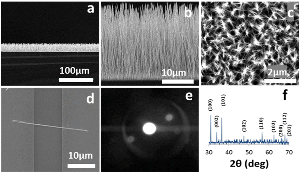 | ||
| Fig. 1 (a) Low magnification side view SEM image, (b) high magnification side view SEM image, (c) top view SEM image of an array of ZNWs; (d) SEM image of a single ZNW, (e) the corresponding SAED pattern of the ZNWs, and (f) the XRD pattern of the ZNWs. | ||
Fig. 2(a–f) present an SEM image, the corresponding SAED pattern, STEM image, XRD pattern, two AFM images of a single ZND, respectively. Most of the exposed facets of the ZND are the polar [0001] surfaces. The XRD pattern and STEM image show that the produced ZNDs are of high crystallinity representing the hexagonal wurtzite-type ZnO (JCPDS No. 36-1451). The AFM analysis shows that the thickness of the grown ZND ranges between 100–150 nm.
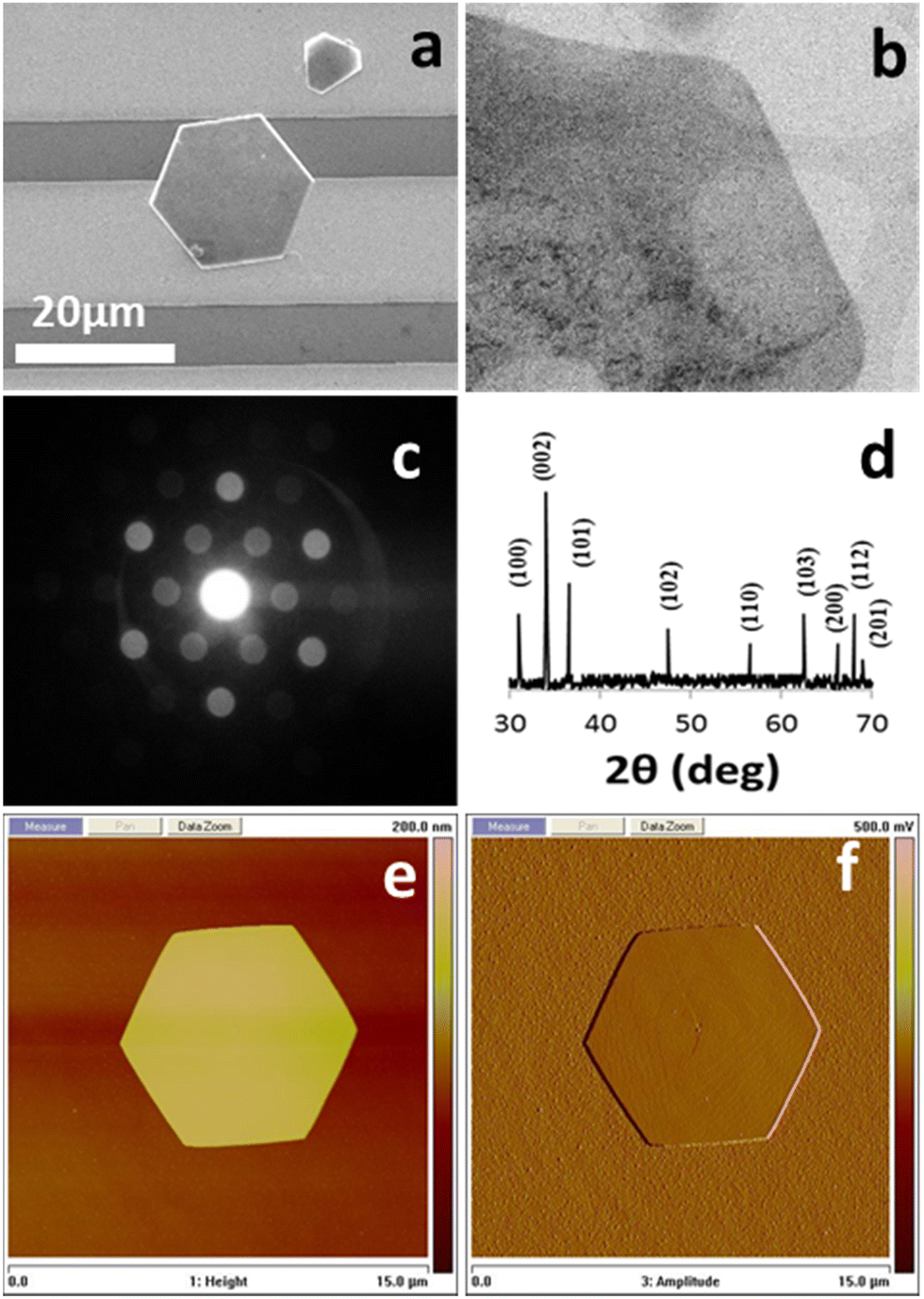 | ||
| Fig. 2 (a) SEM image, (b) the corresponding SAED pattern, (c) STEM image, (d) the XRD pattern, (e), and (f) AFM images of the ZNDs. | ||
As previously reported, hydrothermally grown ZnO nanostructures tend to adopt a 1D form due to the high crystal growth rate in the [0001] direction.30 In addition, in a former report, we learned that the counter-ions of zinc in the hydrothermal growth environment play a key role in shaping the final morphology of the grown nanostructure.15 In the current case of the ZNDs, the charge on the top and bottom facets consists of the positive Zn2+ ions, and so it adsorbs the counter-anions (e.g., SO42−) preferentially instead of the hydroxyl anions. Subsequently, the [Zn(OH)4]2− species required for growth are prevented from reaching the top and bottom facets, forcing the nanostructure to grow sideways instead of the expected intrinsic anisotropic growth along the (0001) direction.30,31
Thus, in the current system, the two mono-morphological ZnO nanostructures produced in the initial growth phase, namely the ZNWs and the ZNDs, were used as seeds in the second growth phase to produce the desired ZNLs and ZNFs, respectively. SEM images at different magnifications of a single and a group of ZNLs grown from initial ZNWs are shown in Fig. 3(a–d). From the SEM analysis, we can see the impact of using zinc sulphate in the second growth phase, which transformed the initial ZNWs into ZNLs by suppressing the axial growth and forcing the initial ZNW to grow sideways. The growth process in the second phase can be described as a process of stretching the initial ZNW thin. The ZNLs consists of very thin sheets with a very high surface-to-volume ratio. The majority of the exposed facets in the ZNLs morphology are the polar (0001) facets. Moreover, another hierarchical ZnO nanostructure, ZNFs, was produced using initial ZNDs as seeds in the second growth phase. Fig. 3(e–h) present SEM images at different magnification of ZNFs. From these images one can see that the ZNFs consists of 2D nanosheet building blocks. The surface-to-volume ratio of the hierarchical ZNFs is clearly higher than that of their mono-morphological counterparts. Indicating that they might have a superior performance as UV PDs. SEM analysis clearly shows that the ZNLs and ZNFs have higher surface-to-volume ratios than their mono-morphological nanostructure counterparts, indicating that they could potentially exhibit superior performances as UV PDs.
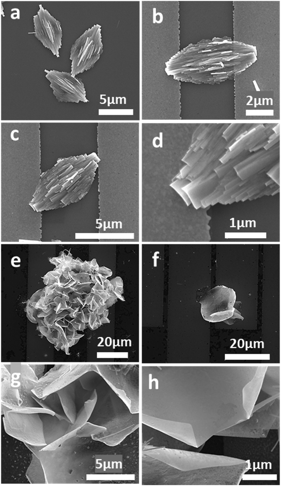 | ||
| Fig. 3 SEM image of (a) several ZNLs, (b and c) a single ZNL connecting two gold electrodes, (d) at high magnification of a single ZNL, (e–h) SEM images at different magnifications of ZNLs. | ||
Following confirmation that ZNLs and ZNFs had been successfully produced, these materials were used to prepare nanostructured ZnO PDs. Similarly, two different ZnO nanostructured PDs were fabricated based on ZNWAs and single ZNWs for comparison with the ZNL- and ZNF-based PDs. The photoresponse characteristics of the ZNWA-, single ZNW-, and ZNL-based PDs are presented in Fig. 4(a–c), respectively, where it can be seen that the photosensitivity of the ZNWA-based PD, which is the ratio of the photocurrent Iph to the dark current Id, was ∼30. In addition, the response and recovery times were 42 and 55 s, respectively. During this study, some of the fabricated ZNWA-based PDs showed relatively long the response and recovery times extending to few minutes. It should be noted here that the conduction channel in the ZNWA-based PD is the seed layer under the ZNWs connecting the two gold electrodes (i.e., a polycrystalline film of ∼300 to 400 nm thickness). As indicated in Fig. 4(a), the photo-response of the ZNWA-based PD exhibits a high stability and repeatability, even though its photosensitivity is low, and the response and recovery times are relatively long. Conversely, the single ZNW-based PD exhibited a photosensitivity of ∼1200, in addition to response and recovery times of 11 and 15 s, respectively. These significant improvements in the photosensitivity and response and recovery times were attributed to a reduction in the dimensionality of the single ZNWs compared with that of the ZNWAs. Moreover, the photo-response characteristics of the ZNL-based PD showed a further enhanced photosensitivity of ∼105, which is four and three orders of magnitude higher than that of the ZNWA-based PD and the ZNW-based PDs, respectively. The response-time and recovery-time of the ZNLs PD are 5 s and 1 s, respectively. The superiority in photosensitivity of ZNLs PD over the other devices stems from the reduction in its dimensions, high surface-to-volume ratio, and the increased percentage of the exposed polar facets. The PDs fabricated based on the ZNFs were also tested but the results from these tests were unreliable. Some ZNFs PDs showed ultrahigh photosensitivity while others were not that sensitive. This could be a result of the morphology and shape of the ZNFs themselves. Looking at their SEM images in Fig. 3, one can see that the sensing material in the ZNFs is not always exposed to the UV radiation. The ZNFs clearly have ultrahigh surface-to-volume ratio making them suitable for sensing applications, but their morphology is not suitable for UV detection.
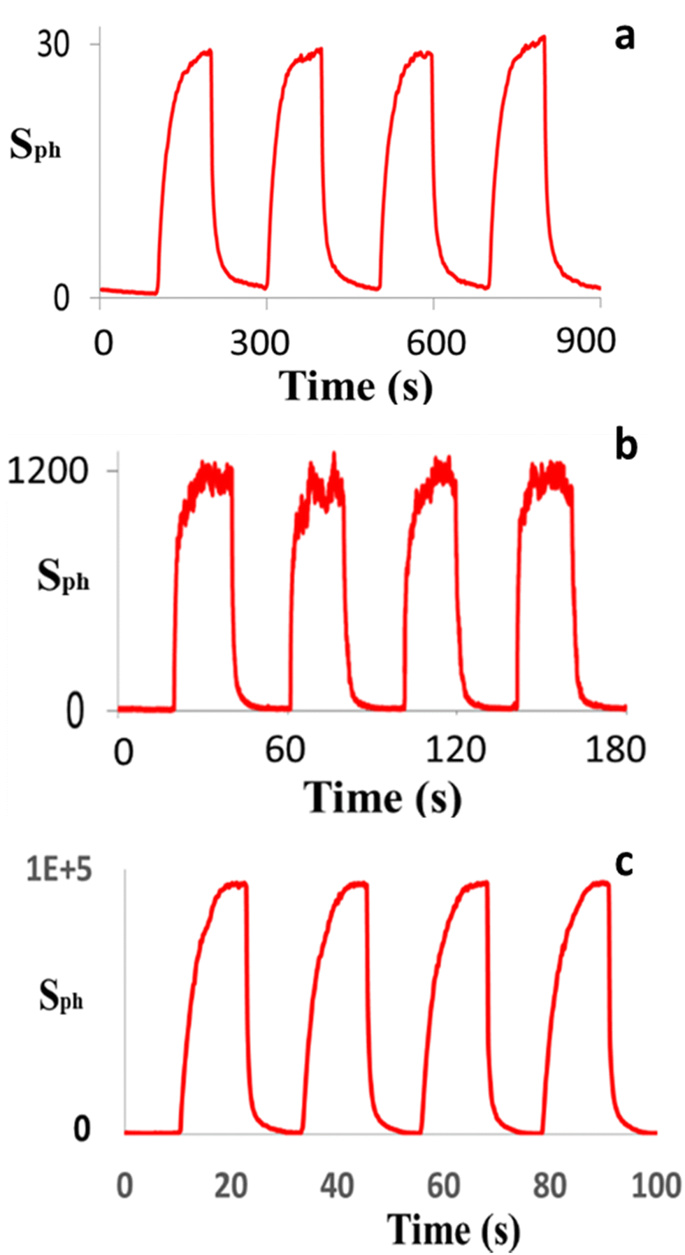 | ||
| Fig. 4 The photo-response characteristics of the (a) ZNWA-based, (b) single ZNW-based, and (c) ZNL-based PDs. | ||
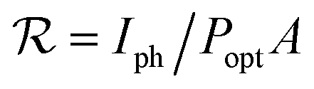
The photoresponsivity represents the ratio of the generated photocurrent to the incident light power on the area of the PD and it is presented in eqn (1).15–19 Using the photocurrent values of 1.2 and 1 nA, and exposed areas of 1 and 12 μm2 for the ZNW and ZNL PDs, respectively; with light power density of 50 μW cm−2 at a wavelength of 365 nm, the calculated photoresponsivity values for the ZNW and ZNL PDs were found to be around 2400 and 166.7 A W−1, respectively.
 | (1) |
The external quantum efficiency ηext representing how many carriers circulate in the detector per adsorbed photon and per unit time, and it is represented as follow:15–19
| ηext = (τ/τt) = (hc/eλ) × (Iph/PoptA) | (2) |
These calculated values of the photoresponsivity and external quantum efficiency are compared with those recently reported in the literature for different inorganic metal oxide nanostructure PDs in Table 1.
| PD |
|
η ext (%) | t response | t recovery | Ref. |
|---|---|---|---|---|---|
| ZnO nanodisk | 3386 A W−1 at 3 V | 1.2 × 10⁴ | 15 s | 65 s | 5 |
| ZnS nanobelt | 0.12 A W−1 at 5 V | 50 | <0.3 s | <0.3 s | 8 |
| ZnO nanofiber arrays homojunction | 1.3 mA W−1 at 0 V | – | 3.9 s | 4.71 s | 9 |
| ZnO–Ga2O3 core–shell heterostructure microwire | 9.7 mA W−1 at 0 V | – | 0.1 ms | 0.9 ms | 10 |
| PANI/ZnO heterojunction | 0.6 mA W−1 at −3 V | – | 0.11 ms | 1.45 ms | 11 |
| BTO–ZnO bilayer film | 1.3 mA W−1 at 3 V | – | 0.1 ms | 5.8 ms | 12 |
| ZnO/NiO heterojunction arrays | 0.4 mA W−1 at 0 V | – | 7.5 s | 4.8 s | 13 |
| TiO2 nanocrystals | 199 A W−1 at 5 V | – | 6 s | 15 s | 18 |
| ZnO hollow-sphere | 13.5 A W−1 at 5 V | – | <5 ms | < 5 ms | 19 |
| p-CuZnS/n-TiO2 nanotube array | 640 A W−1 at 3 V | 2.3 × 10⁵ | <0.2 s | <0.2 s | 20 |
| Sr2Nb3O10 nanosheets | 1214 A W−1 at 3 V | 5.6 × 10⁵ | 0.4 ms | 40 ms | 21 |
| ZnO nanowire | 2400 A W−1 at 2 V | 8160 | 11 s | 15 s | This work |
| ZnO nanoleaves | 166.7 A W−1 at 2 V | 566.8 | 5 s | 1 s | This work |
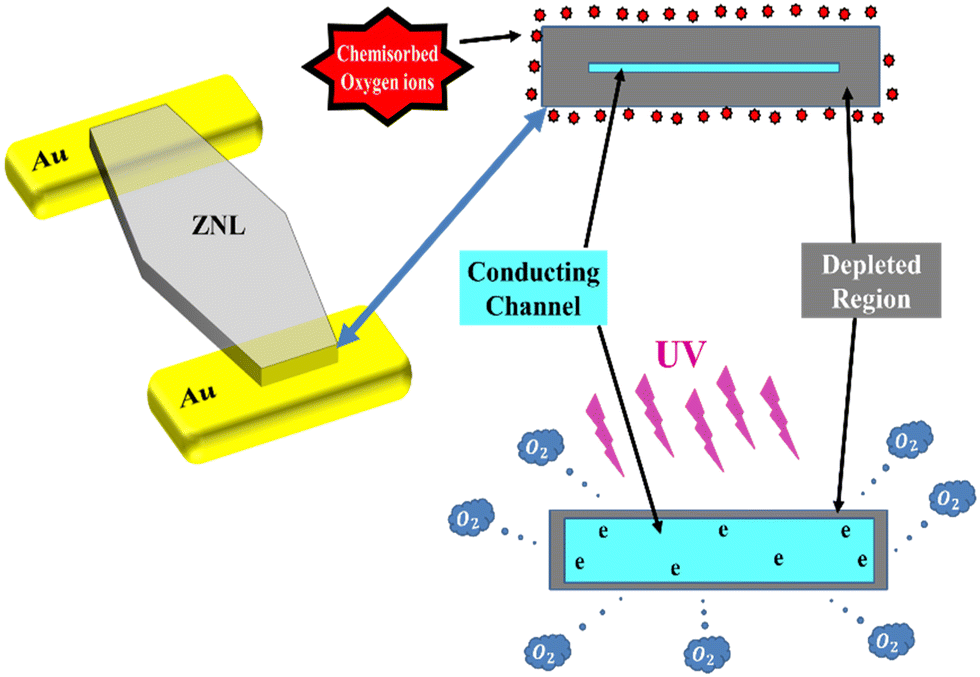
The generation and transportation processes of carriers in the ZNLs PD are explained in the schematic diagram presented in Fig. 5. It should be noted here that due to the presence of oxygen vacancies (VO) in ZnO, which donate electrons to its conduction band, these materials are considered to be n-type semiconductors.35 Thus, in dark and under air, the ZNWs adsorb oxygen molecules on their surfaces, which capture electrons from the conduction band to give oxygen ions (O2−) and create a low-conductivity depletion layer close to the surface. This in turn leads to the creation of band bending due to the negative charge at the surface, which extends the quantum confinement perpendicular to the ZNW surface owing to the quantum size effects. Hence, a surface potential barrier is generated. As a result, under UV irradiation, electron–hole pairs are created in the ZNWs, wherein the holes are attracted to the negatively-charged surface and become trapped:
| hν → e− + h+ | (3) |
| O2−(ad) + h+ → O2(g) | (4) |
 | ||
| Fig. 5 A schematic diagram depicting the carrier generation and transportation processes in the ZNLs UV PDs. | ||
Consequently, the depletion layer becomes narrower under the UV excitation, and the current gradually increases until reaction saturation. Upon ceasing UV irradiation of the ZNWs, electron–hole recombination takes place, causing the oxygen molecules to be re-adsorbed on the ZNW surface. As a result, electrons are recaptured, the depletion layer is widened, and the conductivity of the ZNWs is reduced.35–37 The conductance of the ZNLs can be expressed as:
| G = n0eμπ(R − 2tc)/4l | (5) |
| tc = LD(eVS/kT)1/2 | (6) |
| LD = (εε0kT/e2n0)(1/2) | (7) |
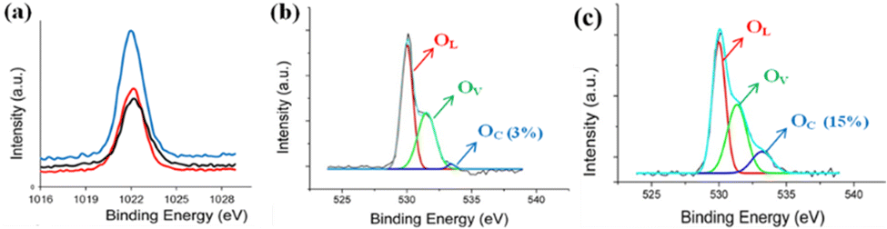
Basically, the UV detection of ZnO nanostructures is an interfacial reaction process, which impacts its conductivity intensively. Hence, the chemical diffusion and readsorption of oxygen molecules occurring on the ZnO surface is a critical factor in its UV photodetection ability. In addition to the impact of the morphology, size, and surface area of ZnO nanostructures on their UV photodetection properties, the exposed polar facets of the ZnO nanostructures may have an important impact and requires more understanding. Hence, the surface structures of as-grown ZnO nanostructures were analyzed by XPS. Fig. 6(a) presents the Zn 2p XPS peaks of the ZNWs and the ZNLs, which appear to be similar for their position and distribution. On the other hand, their corresponding O 1s XPS peaks are similar. Fig. 6(b and c) present the O 1s XPS peaks of the ZNWs and ZNLs, respectively. The two peaks are asymmetric with a visible shoulder. The two O 1s XPS peaks can be decomposed into three Gaussian components centered at ∼530.1 ± 0.15 eV (OL), 531.5 ± 0.2 eV (OV), and 532.5 ± 0.15 eV (OC). Previous studies,42,43 state that the OL component of O 1s spectrum is ascribed to O2− ions on the wurtzite structure of hexagonal Zn2+ ion array, enclosed by zinc atoms with all of their nearest-neighbour O2− ions, meaning that the number of oxygen atoms in a fully oxidised stoichiometric scenario can be evaluated by the intensity of this component. The medium binding energy component OV is related to O2− ions in oxygen-deficient regions in the ZnO matrix, whilst the OC component is typically the result of dissociated and chemisorbed oxygen species or OH. Therefore, an estimation of the oxygen-chemisorbed abilities of different ZnO crystal exposed surfaces can be made on the basis of the intensity of OC components in the O 1s XPS peak. The relative percentages of the OC component in the ZNWs and ZNLs are approximately 3% and 15%, respectively, which indicate that ZNLs may absorb more oxygen species than ZNWs.
 | ||
| Fig. 6 (a) Zn 2p XPS spectra peaks of ZNWs and ZNLs, (b) O 1s XPS spectra of ZNWs, and (c) O 1s XPS spectra of ZNLs. | ||
Conclusions
We herein reported the successful development of a facile and cost-effective hydrothermal synthesis technique for the fabrication of high-performance ZnO nanostructured photodetectors (PDs). The ability to rationally control the morphology and structure of the produced nanostructure was demonstrated by tuning the experimental parameters employed during the growth process. Importantly, the ZnO nanoleaf-based ultraviolet PD (ZNL-based UV PD) demonstrated an ultrahigh photosensitivity (∼105), a good response time (5 s), and a fast recovery time (1 s) compared to other devices prepared using different ZnO nanostructures. The ultrahigh photosensitivity of this system was due to the reduction in size, the ultrahigh surface-to-volume ratio, and increase portion of exposed polar facets compared to those of the other tested mono-morphological nanostructures. Our observations therefore indicate that the hydrothermal technique presented herein should be readily extendable to the low-cost and large-scale fabrication of other practical devices using a range of metal oxides.Conflicts of interest
There are no conflicts to declare.Notes and references
- W. Ouyang, J. Chen, Z. Shi and X. Fang, Self-powered UV photodetectors based on ZnO nanomaterials, Appl. Phys. Rev., 2021, 8, 031315 CAS.
- M. R. Alenezi, et al., Role of the Exposed Polar Facets in the Performance of Thermally and UV Activated ZnO Nanostructured Gas Sensors, J. Phys. Chem. C, 2013, 117, 17850–17858 CrossRef CAS PubMed.
- S. Rehman, R. Ullah, A. M. Butt and N. D. Gohar, Strategies of making TiO2 and ZnO visible light active, J. Hazard. Mater., 2009, 170, 560–569 CrossRef CAS PubMed.
- M. H. Huang, S. Mao and H. Feick, et al., Room-temperature ultraviolet nanowire nanolasers, Science, 2001, 292(5523), 1897–1899 CrossRef CAS PubMed.
- M. R. Alenezi, et al., ZnO Nanodisk based UV Detectors with Printed Electrodes, Langmuir, 2014, 30, 3913–3921 CrossRef CAS PubMed.
- R. C. Wang, H. Y. Lin, C. H. Wang and C. P. Liu, Fabrication of a Large-Area Al-Doped ZnO Nanowire Array Photosensor with Enhanced Photoresponse by Straining, Adv. Funct. Mater., 2012, 22, 3875–3881 CrossRef CAS.
- L. Peng, L. Hu and X. Fang, Low-Dimensional Nanostructure Ultraviolet Photodetectors, Adv. Mater., 2013, 25, 5321–5328 CrossRef CAS PubMed.
- X. Fang, Y. Bando, M. Liao, U. K. Gautam, C. Zhi, B. Dierre, B. Liu, T. Zhai, T. Sekiguchi, Y. Koide and D. Golberg, Single-Crystalline ZnS Nanobelts as Ultraviolet-Light Sensors, Adv. Mater., 2009, 21, 2034–2039 CrossRef CAS.
- Y. Ning, Z. Zhang, F. Teng and X. Fang, Novel Transparent and Self-Powered UV Photodetector Based on Crossed ZnO Nanofiber Array Homojunction, Small, 2018, 14, 1703754 CrossRef PubMed.
- B. Zhao, F. Wang, H. Chen, L. Zheng, L. Su, D. Zhao and X. Fang, An Ultrahigh Responsivity (9.7 mA W−1) Self-Powered Solar-Blind Photodetector Based on Individual ZnO–Ga2O3 Heterostructures, Adv. Funct. Mater., 2017, 27, 1700264 CrossRef.
- Y. Chen, L. Sua, M. Jiang and X. Fang, Switch type PANI/ZnO core-shell microwire heterojunction for UV photodetection, J. Mater. Sci. Technol., 2022, 105, 259–265 CrossRef.
- Y. Zhang, X. Zhao, J. Chen, S. Li, W. Yang and X. Fang, Self-Polarized BaTiO3 for Greatly Enhanced Performance of ZnO UV Photodetector by Regulating the Distribution of Electron Concentration, Adv. Funct. Mater., 2020, 30, 1907650 CrossRef CAS.
- Z. Zhang, Y. Ning and X. Fang, From nanofibers to ordered ZnO/NiO heterojunction arrays for self-powered and transparent UV photodetectors, J. Mater. Chem. C, 2019, 7, 223–229 RSC.
- M. R. Alenezi and A. M. Almeshal, Bridging Nanowires for Enhanced Gas Sensing Properties, Crystals, 2021, 11, 743 CrossRef CAS.
- X. Fang, L. Hu, K. Huo, B. Gao, L. Zhao, M. Liao, P. K. Chu, Y. Bando and D. Golberg, New Ultraviolet Photodetector Based on Individual Nb2O5 Nanobelts, Adv. Funct. Mater., 2011, 21, 3907–3915 CrossRef CAS.
- T. Y. Zhai, M. F. Ye, H. Q. Li, Y. Huang, X. S. Fang, M. Liao, H. S. Zhou, Y. F. Li, Y. Koide, Y. Bando and D. Golberg, Single-crystalline Sb2Se3 nanowires for high-performance field-emitters and photodetectors, Adv. Mater., 2010, 22, 4530–4533 CrossRef CAS PubMed.
- Y. Z. Jin, J. P. Wang, B. Q. Sun, J. C. Blakesley and N. C. Greenham, Solution-Processed Ultraviolet Photodetectors Based on Colloidal ZnO Nanoparticles, Nano Lett., 2008, 8, 1649–1653 CrossRef CAS PubMed.
- H. L. Xue, X. Z. Kong, Z. R. Liu, C. X. Liu, J. R. Zhou, W. Y. Chen, S. P. Ruan and Q. Xu, TiO2 based metal-semiconductor-metal ultraviolet photodetectors, Appl. Phys. Lett., 2007, 90, 201118 CrossRef.
- M. Chen, L. Hu, J. Xu, M. Liao, L. Wu and X. Fang, ZnO Hollow-Sphere Nanofi lm-Based High-Performance and Low-Cost Photodetector, Small, 2011, 7, 2449–2453 CAS.
- X. Xu, J. Chen, S. Cai, Z. Long, Y. Zhang, L. Su, S. He, C. Tang, P. Liu, H. Peng and X. Fang, A Real-Time Wearable UV-Radiation Monitor based on a High-Performance p-CuZnS/n-TiO2 Photodetector, Adv. Mater., 2018, 30, 1803165 CrossRef PubMed.
- S. Li, Y. Zhang, W. Yang, H. Liu and X. Fang, 2D Perovskite Sr2Nb3O10 for High-Performance UV Photodetectors, Adv. Mater., 2020, 32, 1905443 CrossRef CAS PubMed.
- D. Basak, G. Amin, B. Mallik, G. K. Paul and S. K. Sen, Photoconductive UVdetectors on sol–gel-synthesized ZnO films, J. Cryst. Growth, 2003, 256, 73–77 CrossRef CAS.
- J. Wang, B. Weng, P. Larson and Y. Liu, Synthesis and characterization of self-assembled ZnO nanoarrays on hybrid structural fibers, Surf. Interfaces, 2019, 16, 188–193 CrossRef CAS.
- Z. L. Wang, Nanostructures of zinc oxide, Mater. Today, 2004, 7, 26–33 CrossRef CAS.
- J. B. Liang, J. W. Liu, Q. Xie, S. Bai, W. C. Yu and Y. T. Qian, Hydrothermal growth and optical properties of doughnut-shaped ZnO microparticles, J. Phys. Chem. B, 2005, 109, 9463–9467 CrossRef CAS PubMed.
- Y. H. Ni, X. W. Wei, X. Ma and J. M. Hong, CTAB assisted one-pot hydrothermal synthesis of columnar hexagonal-shaped ZnO crystals, J. Cryst. Growth, 2005, 283, 48–56 CrossRef CAS.
- U. Pal and P. Santiago, Controlling the Morphology of ZnO Nanostructures in a Low-Temperature Hydrothermal Process, J. Phys. Chem. B, 2005, 109, 15317–15321 CrossRef CAS PubMed.
- M. Oner, J. Norwig, W. H. Meyer and G. Wegner, Control of ZnO crystallization by a PEO-b-PMAA diblock copolymer, Chem. Mater., 1998, 10, 460–463 CrossRef.
- F. Li, Y. Ding, P. Gao, X. Xin and Z. L. Wang, Single-Crystal Hexagonal Disks and Rings of ZnO: Low-Temperature, Large-Scale Synthesis and Growth Mechanism, Angew. Chem., Int. Ed., 2004, 43, 5238–5242 CrossRef CAS PubMed.
- M. R. Alenezi, et al., Hierarchically Designed ZnO Nanostructures Based High Performance Gas Sensors, RSC Adv., 2014, 4, 49521–49528 RSC.
- M. R. Alenezi, S. J. Henley, N. G. Emerson and S. R. P. Silva, From 1D and 2D ZnO nanostructures to 3D hierarchical structures with enhanced gas sensing properties, Nanoscale, 2014, 6, 235–247 RSC.
- M. R. Alenezi, S. J. Henley and S. R. P. Silva, On-chip Fabrication of High Performance Nanostructured ZnO UV Detectors, Sci. Rep., 2015, 5, 8516 CrossRef PubMed.
- M. R. Alenezi, Hierarchical zinc oxide nanorings with superior sensing properties, Mater. Sci. Eng., B, 2018, 236, 132–138 CrossRef.
- M. R. Alenezi, T. H. Alzanki, A. M. Almeshal, A. S. Alshammari, M. J. Beliatis, S. J. Henley and S. R. P. Silva, A model for the impact of the nanostructure size on its gas sensing properties, RSC Adv., 2015, 5, 103195 RSC.
- C. C. Lin, S. Y. Chen, S. Y. Cheng and H. Y. Lee, Properties of nitrogen-implanted p-type ZnO films grown on Si3 N4/Si by radio-frequency magnetron sputtering, Appl. Phys. Lett., 2004, 84, 5040–5042 CrossRef CAS.
- T. Tachikawa, M. Fujitsuka and T. Majima, Mechanistic Insight into the TiO2 Photocatalytic Reactions:
![[thin space (1/6-em)]](https://www.rsc.org/images/entities/char_2009.gif) Design of New Photocatalysts, J. Phys. Chem. C, 2007, 111, 5259–5275 CrossRef CAS.
Design of New Photocatalysts, J. Phys. Chem. C, 2007, 111, 5259–5275 CrossRef CAS. - L. Peng, et al., Ultraviolet-assisted gas sensing: A potential formaldehyde detection approach at room temperature based on zinc oxide nanorods, Sens. Actuators, B, 2009, 136, 80–85 CrossRef CAS.
- V. V. Sysoev, B. K. Button, K. Wepsiec, S. Dmitriev and A. Kolmakov, Toward the Nanoscopic “Electronic Nose”: Hydrogen vs Carbon Monoxide Discrimination with an Array of Individual Metal Oxide Nano- and Mesowire Sensors, Nano Lett., 2006, 6, 1584–1588 CrossRef CAS PubMed.
- J. Zhou, et al., Gigantic enhancement in response and reset time of ZnO UV nanosensor by utilizing Schottky contact and surface functionalization, Appl. Phys. Lett., 2009, 94, 191103 CrossRef PubMed.
- A. Umar, B. K. Kim, J. J. Kim and Y. B. Hahn, Optical and electrical properties of ZnO nanowires grown on aluminium foil by non-catalytic thermal evaporation, Nanotechnology, 2007, 18, 175606 CrossRef.
- C. Yan, N. Singh and P. S. Lee, Wide-bandgap Zn2GeO4 nanowire networks as efficient ultraviolet photodetectors with fast response and recovery time, Appl. Phys. Lett., 2010, 96, 053108 CrossRef.
- P. T. Hsieh, Y. C. Chen, K. S. Kao and C. M. Wang, Luminescence mechanism of ZnO thin film investigated by XPS measurement, Appl. Phys. A: Mater. Sci. Process., 2008, 90, 317–321 CrossRef CAS.
- M. Chen, X. Wang, Y. H. Yu, Z. L. Pei, X. D. Bai, C. Sun, R. F. Huang and L. S. Wen, X-ray photoelectron spectroscopy and auger electron spectroscopy studies of Al-doped ZnO films, Appl. Surf. Sci., 2000, 158, 134 CrossRef CAS.
| This journal is © The Royal Society of Chemistry 2022 |