DOI:
10.1039/D2MA00503D
(Paper)
Mater. Adv., 2022,
3, 6566-6576
In situ CsPbBr3 architecture engineered in electrospun fibers and its ultrafast charge-transfer dynamics†
Received
4th May 2022
, Accepted 5th July 2022
First published on 6th July 2022
Abstract
All-inorganic lead halide perovskite nanocrystals (NCs) have witnessed a rapid progression in the field of optoelectronics as well as photovoltaic applications. However, their environmental instability, tedious synthesis protocols, and post treatments hinder their further development for energy-harvesting devices. However, the aforementioned obstacles can be easily tackled by engineering them with a piezoelectric polymer, in situ perovskite construction, and by encapsulation. To date, the fundamental photophysical study of piezoelectric polymers with perovskite materials is still in early phase, and deeper understanding could illustrate a road map for their further advancement in solar cells and photodetectors, which is the main focus of this study. Herein, we present a facile route for the synthesis of highly stable cesium lead bromide (CsPbBr3) inside poly(vinylidene fluoride)-co-hexafluoropropylene (PVDF-HFP) fibers using a single step in situ electrospinning technique. X-Ray diffraction analysis depicted the successful formation of the β-phase in PVDF-HFP along with CsPbBr3 during the electrospinning process. High-resolution transmission electron microscopy (HR-TEM) images clearly evidenced the arrangement of CsPbBr3 inside the fiber matrix. Moreover, the synthesized CsPbBr3@PVDF-HFP fibers exhibited narrow light emission, which supported the optical and structural analysis. To understand the charge-transfer process in the CsPbBr3@PVDF-HFP fibers, transient absorption (TA) spectroscopy was employed. Different pump excitations were employed to identify the carrier-relaxation mechanism in the type-I CsPbBr3@PVDF-HFP fiber architecture. TA spectroscopy studies clearly suggested the transfer of charge carriers from CsPbBr3 to PVDF-HFP upon 300 nm pump excitation, which was a thermodynamically viable process. Our results provide a facile and effective strategy for the preparation of a stable perovskite architecture and an in depth study of the photophysical properties, which could provide significant assistance in the development of highly efficient perovskite-based solar cell and photodetector applications.
Introduction
The rapid emergence of optoelectronic devices based on all-inorganic metal halides (CsPbX3, X = Cl, Br, I) perovskite materials have attracted tremendous interest owing to their tunable photoluminescence (PL) across the whole visible spectrum (400–700 nm), high PL quantum yield (QY), narrow emission width, and fast carrier diffusion.1,3 However, perovskite materials have some obstacles, including poor stability against water and polar solvents, as drawbacks that largely limit their practical applicability.4,5 Thus number of methods have been explored to stabilize the perovskite nanomaterials encapsulated with other matrices, including silica, zirconia, and polymers for the applications of light-emitting diodes (LED), visible-light communication, and X-ray scintillators.6–9 As a state-of-the-art technique, electrospinning is considered one of the most effective techniques to prepare nanocrystalline fibers.10 Moreover, nanofibers can act as an effective support for the functional materials, including metal nanoparticles and quantum dots (QDs) nanocrystals. Polyvinyl pyrrolidone (PVP), poly(methyl methacrylate) (PMMA), and polystyrene (PS) polymers have been efficiently utilized for the synthesis of perovskite nanofibers and these are highly stable under ambient atmosphere. Moreover, these materials are not suitable for energy-harvesting purposes owing to the insulating nature of aforementioned polymers.11–13 Polyvinylidene fluoride (PVDF) is one of the well-known piezoelectric polymers that have great potential for use in mechanical energy-harvesting techniques, sensors, and biomedical applications due to its lightweight, soft, and biocompatible nature.14,15 Moreover, PVDF being a semicrystalline polymer resides in five crystalline phases in nature, i.e., α, β, γ, δ, and ε. Amid these phases, the β and γ phase are polar in nature and in the electroactive forms, particularly the β phase, which exhibits piezoelectric, pyroelectric, and ferroelectric properties.14–17 Moreover, PVDF polymer is hydrophobic in nature and it can effectively prevent the degradation of CsPbBr3 from polar solvents, which would improve the stability. Wang et al. in situ-encapsulated CsPbBr3 spheres using an electrospray method with polyvinylidene fluoride for cell-imaging applications.18 Further, unusual stability and temperature-dependent properties have been reported by Pan and co-workers.19 Recently, piezoelectric nanogenerators have been widely reported with PVDF along with different types of perovskites. In addition to that, Sultana et al. demonstrated improvements in the photocurrent could be achieved with the use of a methylammonium lead iodide (CH3NH3PbI3) and β-phase poly(vinylidene fluoride) composite.20 Improved acoustic nanogenerators comprising methylammonium lead bromide (CH3NH3PbBr3) and poly(vinylidene fluoride) (PVDF) nanofibers were reported by Mandal and co-workers using an electrospinning process.21
The improved photocurrent in the aforesaid materials could be due to the formation of a high degree of β-phase formation. The β-phase in the PVDF matrix is nucleated by perovskite QDs using surface electrostatic interaction to transform the α phase into the β-phase. Fang et al. incorporated PVDF-HFP into CH3NH3PbI3 solution for solar-cell applications and found that PVDF-HFP could improve the carrier lifetimes and reduce the charge-transfer resistance, which could collectively enhance the solar-cell efficiency.22 Moreover, upon the excitation of perovskite nanocrystals, excitons were created within the nanocrystals, which further improved the polarizability in the PVDF polymer, reducing the electron–hole recombination and increase the charge transfer.20–22 These results clearly evidenced that these materials could prove to be an asset for optoelectronic applications.
In addition, Dong et al. synthesized CsPbBr3/PVP fibers using a microfluidic electrostatic spinning method. However, the microfluidic electrostatic spinning technique could not meet the high-rate throughput of fibers owing to the strict standards on the precursor materials.23 Further, Cheng's group developed in situ methylammonium lead halide (MAPbX3, X = Cl, Br, and I) perovskite at a large scale inside polyacrylonitrile (PAN) nanofiber films based on a microfluidic blow spinning (MBS) technique.24 This method influenced the unique advantages, including mild reaction conditions, straightforward operation, low cost, and scalability. However, even a small variation in the polymer concentration, gas pressure, viscosity, and flow rate could lead to capillary instability, dripping, clogging, and fly formation, strictly affecting the continuous fiber formation.25 Importantly, the electrospinning process can effectively circumvent the aforesaid demerits and support the development of the in situ architecture of CsPbBr3 along with the formation of the β-phase in PVDF-HFP fibers.
So far, only limited reports are available in the literature on this subject, which might be due to the lack of fundamental evidence present in the earlier reports. The limited knowledge regarding the photophysical aspects of these polymer-embedded perovskite seems to be a hindrance to the further development progress of these polymer–perovskite-based photovoltaics. In order to make progress, the profound physical properties of the perovskite-encapsulated PVDF matrix should be addressed, which could assist in effective device fabrication. The charge-carrier dynamics, including charge separation, carrier relaxation, and carrier transfer, and recombination processes occur within the sub-picosecond time scale and can be studied employing transient absorption (TA) spectroscopy, which should also motivate further improvements for practical device applications.26–28 In the present study, we synthesized CsPbBr3 inside polymer fibers based on a one-step in situ electrospinning strategy. To the best of our knowledge, there has been no detailed study of the charge-carrier dynamics in confined media, especially perovskite nanoparticles embedded in piezoelectric PVDF-HFP fibers. Consequently, we investigated the charge-carrier dynamics of in situ-encapsulated CsPbBr3 in a PVDF-HFP polymer matrix using transient absorption spectroscopic studies to explore the possibilites for application in highly efficient solar cells and photodetectors.
Results and discussion
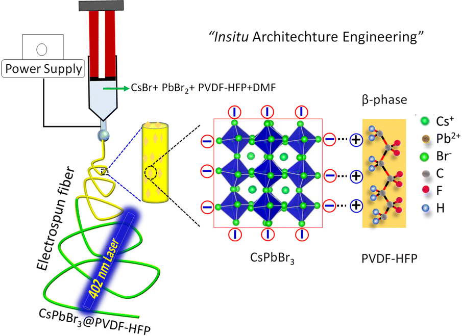
A single solution containing PVDF-HFP, CsBr, and PbBr2 was dissolved in DMF (details in the ESI†) prior to the formation of electrospun fibers. During the electrospinning, the tip of the needle was dipped in to a solution containing PVDF-HFP, Cs+, Pb2+, and Br− ions, for drawing the solution into a cone-like structure, termed a Taylor cone, under a high electric field. Then the solution was stretched along the axis due to the charge accumulation followed by repulsion of the charges. The in situ growth of CsPbBr3 inside the fibers took place with simultaneous solvent evaporation and the fiber was collected on the drum collector (Fig. 1).
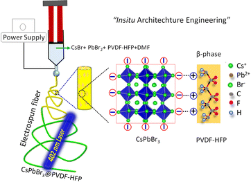 |
| | Fig. 1 Schematic illustration for the in situ growth of CsPbBr3 in the PVDF-HFP polymers via a one-step electrospinning method. | |
In situ CsPbBr3 architecture engineering in electrospun PVDF-HFP fibers
The in situ formation mechanism of CsPbBr3 along with the formation of the β-phase in PVDF-HFP during the electrospinning process are schematically represented in Fig. 1. Commonly, the bare PVDF-HFP exhibits the α-phase owing to its random orientation of dipoles that leads to net average polarization, represented as a non-polar phase. Owing to its aforesaid characteristics, the α-phase of PVDF-HFP fails to produce piezo- and pyroelectric properties. On the other hand, the β-phase, in which the molecular dipoles are entirely aligned in one direction, generates spontaneous polarization, which makes the non-polar phase useful for a wide range of applications. However, β-phase formation needs the use of expensive and tedious techniques, including poling, mechanical stretching, and ball milling. Among these, electrospinning results in a partial phase transition to the polar β-phase. In order to enhance the polarizability number, fillers have been utilized that electrostatically interact with –CF2 or –CH2 units that can nucleate the polar phase, which promotes the superior piezo- and pyroelectric properties. Recently, perovskite materials have been efficiently used for optoelectronic as well as photovoltaic applications.20–22 Owing to their ionic nature, perovskite materials easily degrade with moisture and polar solvents, which hinders their practical applications. To improve the stability as well as the feasibility of utilizing perovskites, such materials have been engineered with a piezoelectric polymer matrix. Here, the electrospinning technique was concurrently used for the formation of the polar β-phase along with the in situ formation of CsPbBr3. In situ-formed CsPbBr3 acted as the filler for the polar phase formation along with the electrospinning. Moreover, we did not utilize any ligands for the formation of CsPbBr3 NCs, yet the in situ-synthesized CsPbBr3 NCs maintained better optical as well as structural stability compared to that prepared with traditional methods. The CsPbBr3 comprises three-dimensional (3D) corner-shared [PbBr6] octahedra and Cs cations that stabilize the structure. Moreover, the electronegative bromine atoms of the [PbBr6]4− octahedra provide the negative charge density that electrostatically interacts with the –CH2 dipoles (positively charged). The aforesaid interaction helps to nucleate the polar phases during the electrospinning process. In addition, the formation of the electroactive β-phase mainly arises due to the strong electrostatic interaction between the [PbBr6]4− and –CH2 dipoles (Fig. 1).20 In addition, the in situ-synthesized CsPbBr3 NCs act as the filler to engineer the β-phase formation of PVDF-HFP fibers, which may help to enhance the photovoltaic properties and stability compared to that of traditional CsPbBr3 NCs. Finally, the in situ formation of CsPbBr3 NCs with the β-phase PVDF-HFP fiber can be termed as a form of in situ architecture engineering.
XRD patterns
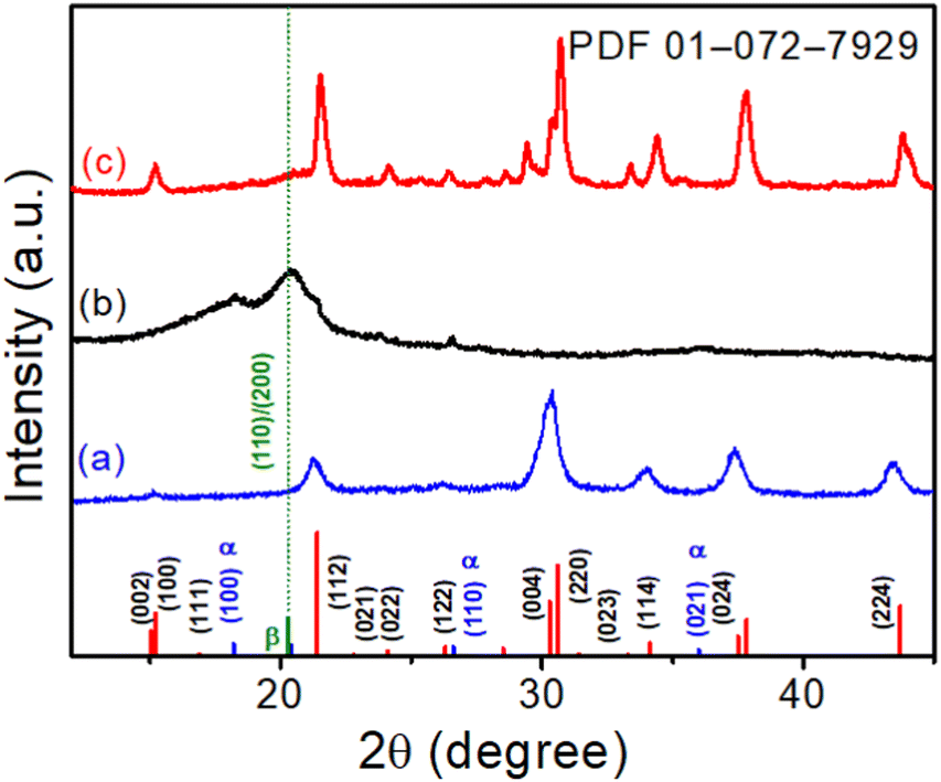
XRD patterns were utilized to evaluate the crystallographic structure and phase purity of the CsPbBr3 NCs, electrospun PVDF-HFP fiber, and CsPbBr3@PVdF-HFP fiber. The XRD pattern of CsPbBr3 NCs (for comparison), electrospun PVDF-HFP fiber, and CsPbBr3@PVDF-HFP fiber are depicted in Fig. 2. The XRD peaks of CsPbBr3 NCs were well defined and belonged to the orthorhombic phase and were in good agreement with the standard JCPDS (PDF-01-0172-7929) values (Fig. 2a).19,28 The bare electrospun PVDF-HFP fiber exhibited peaks at 18.2°, 20.4°, 26.6°, and 36.6°, corresponding to the diffractions of the (100), (020), (110), and (021) planes of the α, β crystalline phases (Fig. 2b).29,30 The CsPbBr3@PVDF-HFP fiber retained the above-mentioned planes for PVDF-HFP along with additional diffraction planes. The noticed additional main peaks were at 14.9°, 15.1°, 21.3°, 21.5°, 30.2°, 30.5°, and 37.5° (Fig. 2c) and corresponded to the (002), (110), (112), (200), (004), (220), and (312) reflection planes of CsPbBr3. The characteristic diffraction planes ensured the orthorhombic phase CsPbBr3 with the Pnma space group. Moreover, the diffraction peaks at 19.2° (002) and 20.8° (110/200) were ascribed to the presence of the γ- and β-phase, respectively.29,30 These results clearly confirmed the in situ formation of CsPbBr3 along with the formation of the β-phase in PVDF-HFP during the electrospinning process (Fig. 2c). Importantly, CsPbBr3@PVDF-HFP fiber did not contain any other phases, including CsPb2Br5 and Cs4PbBr6, as evidenced from our XRD analysis.31 Furthermore, the FT-IR spectrum of CsPbBr3–PVdF-HFP fiber showed characteristic peaks at 841 and 1278 cm−1 (Fig. S2a, ESI†), corresponding to the β-phase,21 which supported the XRD observation.
 |
| | Fig. 2 XRD patterns of (a) CsPbBr3 NCs, (b) electrospun PVDF-HFP fiber, and (c) CsPbBr3@PVDF-HFP fiber, with the orthorhombic CsPbBr3 JCPDS values marked at the bottom. | |
Microscopy studies of CsPbBr3@PVDF-HFP fiber
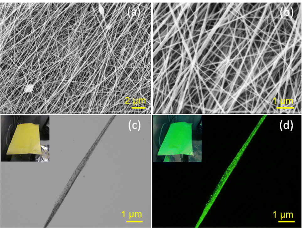
The SEM images of CsPbBr3@PVDF-HFP fibers are shown in Fig. 3a and b. The electrospun mats were highly interconnected with a randomly oriented fibrous morphology. The surface of the individual CsPbBr3@PVDF-HFP fiber was highly uniform and smooth. In addition, no defects or cracks were noticed on the surface of the CsPbBr3@PVDF-HFP fiber, indicating that the PVDF-HFP fiber did not become brittle after the in situ CsPbBr3 formation. The CsPbBr3@PVDF-HFP fibers exhibited an average diameter of 600–800 nm and length of several millimeters (Fig. 3a and b). Next, energy-dispersive X-ray spectroscopy (EDS) was performed to establish the CsPbBr3 in the CsPbBr3@PVDF-HFP fibers through elemental analysis by evaluating the Cs, Pb, and Br elements. The EDS pattern of CsPbBr3@PVDF-HFP fiber showed it was composed of C, F, Cs, Pb, and Br. The ratio of 1![[thin space (1/6-em)]](https://www.rsc.org/images/entities/char_2009.gif) :1:3 was maintained for Cs, Pb, and Br with the stoichiometry of CsPbBr3 after the electrospinning method (Fig. S2b, ESI†). The elemental distribution of the electrospun CsPbBr3@PVDF-HFP fiber was determined through elemental mapping. The mapped red, blue, cyan, green, and pink colored regions corresponded to C, F, Cs, Pb, and Br elements, respectively, representing the homogeneous distribution of CsPbBr3 inside the electrospun PVDF-HFP fiber (Fig. S3, ESI†). An optical image of the CsPbBr3@PVDF-HFP fiber showed smooth, transparent, and black particles. The corresponding fluorescent image displayed green light emission along the fibers, which clearly suggested the in situ formation of CsPbBr3 inside the PVDF-HFP fiber matrix (Fig. 3c and d). The internal morphology of the embedded CsPbBr3 over PVDF-HFP fibers was further evaluated via transmission electron microscopy (TEM) and the results are depicted in Fig. 4. The average diameter of the electrospun CsPbBr3@PVDF-HFP fibers matched exactly with the SEM observation and it showed a fiber length of several nanometers (Fig. 4a and b). Owing to the higher thickness of the fibers, the particles were not properly visible, but in the walls of the fibers small particles of CsPbBr3 were visible. The interior structure of the CsPbBr3@PVDF-HFP fibers was further explored via high-resolution TEM (Fig. 4c and d). From that, it could be seen that CsPbBr3 was homogeneously formed inside the PVDF-HFP fiber matrix. During the electrospinning process, in situ CsPbBr3 was formed and it was encapsulated by the PVDF-HFP fibers (Fig. 4c). The average crystallite size was calculated using the Scherrer formula from the most intense diffraction peak (220) of CsPbBr3 and was found to be around ∼21.4 nm (Fig. 4c). The HR-TEM images clearly revealed the (110) plane of orthorhombic CsPbBr3 with an interplanar spacing of 0.58 nm, confirming the formation of in situ orthorhombic CsPbBr3 (Fig. 4d).31 The aforementioned results matched exactly with the XRD data. The pristine CsPbBr3 NCs displayed a cubic morphology with an average size of 12 nm and showed a typical d spacing (110 plane) of 0.58 nm, confirming the orthorhombic phase of CsPbBr3 (Fig. S1a and b, ESI†).
:1:3 was maintained for Cs, Pb, and Br with the stoichiometry of CsPbBr3 after the electrospinning method (Fig. S2b, ESI†). The elemental distribution of the electrospun CsPbBr3@PVDF-HFP fiber was determined through elemental mapping. The mapped red, blue, cyan, green, and pink colored regions corresponded to C, F, Cs, Pb, and Br elements, respectively, representing the homogeneous distribution of CsPbBr3 inside the electrospun PVDF-HFP fiber (Fig. S3, ESI†). An optical image of the CsPbBr3@PVDF-HFP fiber showed smooth, transparent, and black particles. The corresponding fluorescent image displayed green light emission along the fibers, which clearly suggested the in situ formation of CsPbBr3 inside the PVDF-HFP fiber matrix (Fig. 3c and d). The internal morphology of the embedded CsPbBr3 over PVDF-HFP fibers was further evaluated via transmission electron microscopy (TEM) and the results are depicted in Fig. 4. The average diameter of the electrospun CsPbBr3@PVDF-HFP fibers matched exactly with the SEM observation and it showed a fiber length of several nanometers (Fig. 4a and b). Owing to the higher thickness of the fibers, the particles were not properly visible, but in the walls of the fibers small particles of CsPbBr3 were visible. The interior structure of the CsPbBr3@PVDF-HFP fibers was further explored via high-resolution TEM (Fig. 4c and d). From that, it could be seen that CsPbBr3 was homogeneously formed inside the PVDF-HFP fiber matrix. During the electrospinning process, in situ CsPbBr3 was formed and it was encapsulated by the PVDF-HFP fibers (Fig. 4c). The average crystallite size was calculated using the Scherrer formula from the most intense diffraction peak (220) of CsPbBr3 and was found to be around ∼21.4 nm (Fig. 4c). The HR-TEM images clearly revealed the (110) plane of orthorhombic CsPbBr3 with an interplanar spacing of 0.58 nm, confirming the formation of in situ orthorhombic CsPbBr3 (Fig. 4d).31 The aforementioned results matched exactly with the XRD data. The pristine CsPbBr3 NCs displayed a cubic morphology with an average size of 12 nm and showed a typical d spacing (110 plane) of 0.58 nm, confirming the orthorhombic phase of CsPbBr3 (Fig. S1a and b, ESI†).
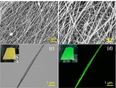 |
| | Fig. 3 (a and b) SEM images of CsPbBr3@PVDF-HFP fiber, (c) optical microscopic and (d) fluorescence images of a single strand of CsPbBr3@PVDF-HFP fiber (inset: corresponding photographic images of a CsPbBr3@PVDF-HFP fiber mat deposited over aluminum foil). | |
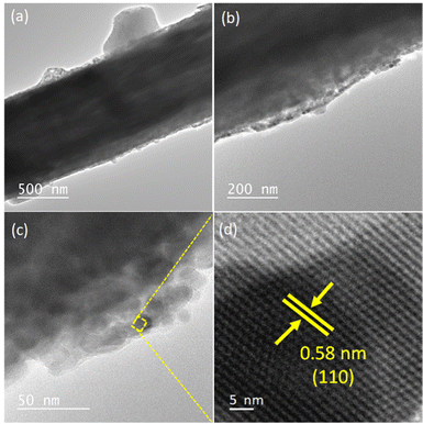 |
| | Fig. 4 (a and b) TEM and (c and d) HR-TEM images of the CsPbBr3@PVDF-HFP fiber. | |
XPS analysis
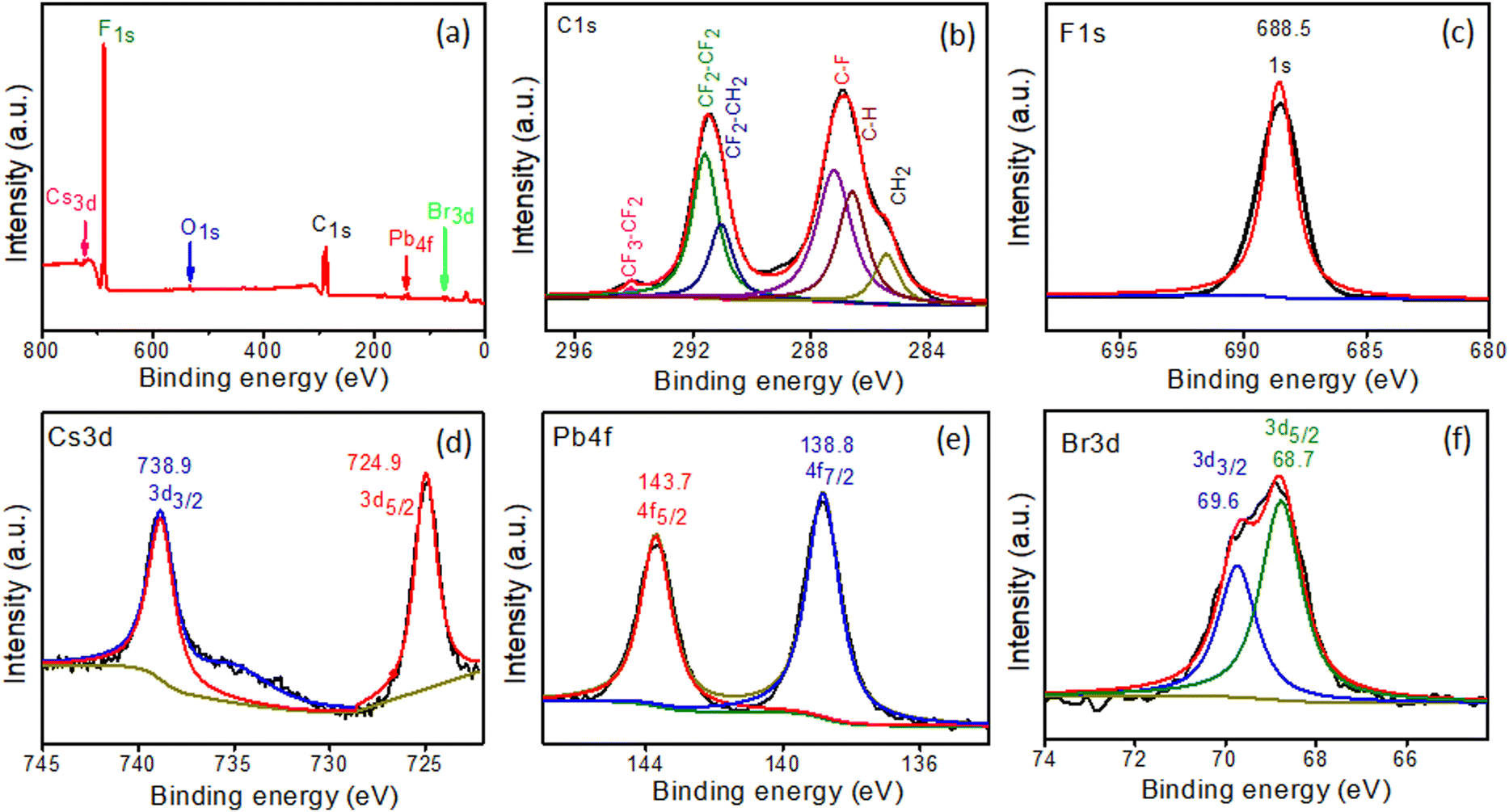
XPS spectra of in situ-synthesized samples were obtained to evaluate the oxidation states and chemical compositions of the PVDF-HFP@CsPbBr3 fiber. The signals of C, F, Cs, Pb, and Br from the survey spectrum were constituent elements of the PVDF-HFP polymer and CsPbBr3 (Fig. 5a).29–32 The PVDF-HFP polymer exhibited very strong peaks related to C and F, which were the constituents of the polymer backbone. The core C1s spectrum was fitted with six peaks with binding energies of 285.5, 286.6, 287.2, 291, 291.5, and 294.1 eV, corresponding to CH2, C–H, C–F, CF2–CH2, CF2–CF2 and CF3–CF2 respectively and the binding energy at 688.5 eV was related to F1s (Fig. 5b and c).32 Further, Cs3d5/2 and Cs3d3/2 appeared as two peaks centered at 724.8 and 738.9 eV, respectively (Fig. 5d). The spectrum of Pb 4f showed binding energies of 138.8 and 143.7 eV, corresponding to 4f7/2 and 4f5/2 (Fig. 5e). In addition, peaks for Br 3d5/2 and Br 3d3/2 were displayed at 68.7 and 69.7 eV, confirming the in situ formation of CsPbBr3 in the PVDF-HFP fiber matrix (Fig. 5f).33–35
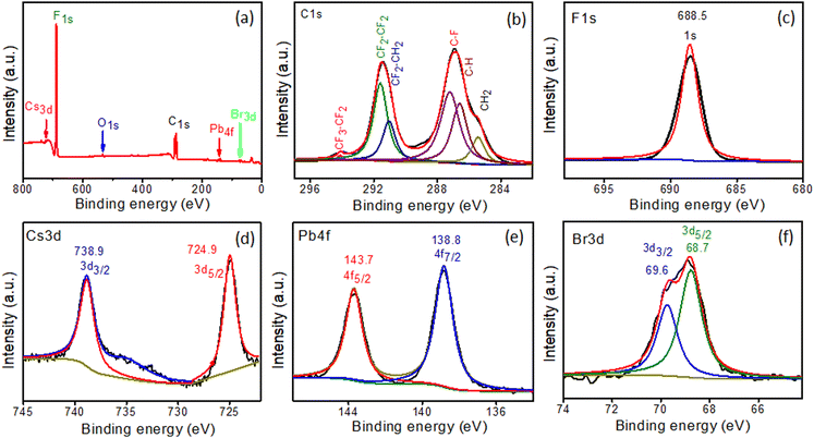 |
| | Fig. 5 XPS spectra of PVDF-HFP@CsPbBr3 fiber: (a) survey scan and high-resolution scans of (b) C1s, (c) F1s, (d) Cs3d, (e) Pb4f, and (f) Br3d. | |
Optical studies
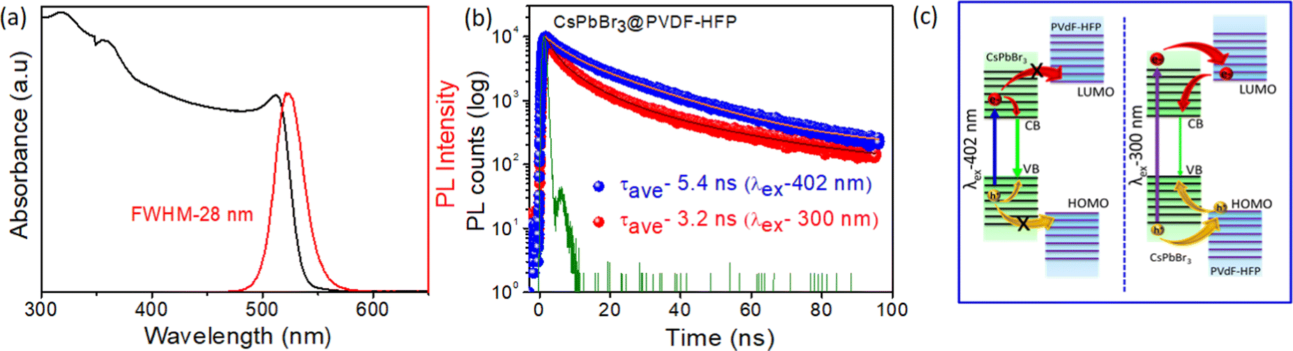
To further study the synthesized materials properties, optical absorption and steady-state photoluminescence (PL) spectroscopy were performed at room temperature. Fig. 6a and Fig. S1c (ESI†) show the optical properties of CsPbBr3 NCs dispersed in toluene (for comparison) and CsPbBr3@PVDF-HFP fiber. The CsPbBr3 NCs and in situ-synthesized CsPbBr3@PVDF-HFP fiber exhibited a clear first excitonic absorption peak at 506 nm, 514 nm, and sharp band edge PL peak (λex = 420 nm) at 516 nm, 524 nm, respectively. The full width at half-maximum (FWHM) was calculated to be 18 and 28 nm for CsPbBr3 NCs and CsPbBr3@PVDF-HFP fiber, respectively. Further, a small Stokes shift appeared (10 nm) for both samples, implying that the PL emission of CsPbBr3 originated from direct exciton recombination.2,3 The PL quantum yield (PLQY) was calculated to be 30% and 70% for CsPbBr3@PVDF-HFP fiber and CsPbBr3 NCs, respectively (Fig. S4 and Table S1, ESI†). The core–shell CsPbBr3@PVDF-HFP fiber exhibited a type-I band alignment and the PLQY of CsPbBr3@PVDF-HFP fiber was decreased compared to that of CsPbBr3 NCs, which might be due to some unavoidable agglomeration of the CsPbBr3 or some interfacial trap states.13 The excited state behaviors of the CsPbBr3@PVDF-HFP fiber and CsPbBr3 NCs were evaluated using time resolved emission measurements. The PL emission decay at 524 and 516 nm was monitored for CsPbBr3@PVDF-HFP fiber and CsPbBr3 NCs, respectively. Both the samples were excited with a 402 and 300 nm laser pulse and the corresponding PL decay was plotted (Fig. 6b and Fig. S1b, ESI†). Fig. S1b (ESI†) presents the PL decay trace of CsPbBr3 NCs in toluene after exciting the sample at 300 and 402 nm and monitoring the emission at 516 nm. It can be clearly seen that the PL lifetimes for both excitations were very similar at ∼8.2 and 6.8 ns. This observation clearly suggested that the PL lifetime of CsPbBr3 NCs in toluene is independent of the excitation. However, the average PL decay lifetime for CsPbBr3@PVDF-HFP fiber was found to be 5.4 and 3.2 ns for (λex) 402 and 300 nm, respectively (Fig. 6b). Here, with the PVDF-HFP fiber acting as the protecting shell for the in situ-synthesized CsPbBr3 it also provided a large band offset, which led to this type I band alignment. In accordance with this band alignment, for 402 nm excitation, the incident photons were capable of exciting the charge carriers only within the band gap of CsPbBr3 but the photogenerated carriers did not have sufficient energy to cross over to PVDF-HFP due to the large band offset of the PVDF-HFP polymer compared to CsPbBr3. However, this was not the situation with 300 nm excitation, where photoexcited carriers were generated in both the CsPbBr3 core and PVDF-HFP shell. The decrement in the PL decay for CsPbBr3@PVDF-HFP fiber at 300 nm over that of 402 nm could thus attributed to the thermodynamically viable delocalization of charge carriers (electron/hole) among the levels of CsPbBr3 and PVDF-HFP in the former case (Fig. 6c (right panel)) and the subsequent inevitable loss of some of the carriers in this process as a consequence of trapping at the interface of the CsPbBr3 and fiber. It was interesting to see that the PL lifetime of CsPbBr3 in the PVDF-HFP fiber was much lower compared to that of CsPbBr3 NCs in toluene. This might be due to the unavoidable trapping of charge carriers between the PVDF-HFP fiber and CsPbBr3 interface.13 From the above studies, it was confirmed that the CsPbBr3@PVDF-HFP fiber showed charge delocalization behavior at 300 nm excitation. However, as the PL lifetime setup in our laboratory has a nanosecond time resolution, it was difficult for us to monitor the accurate charge-transfer dynamics, including the carrier relaxation and carrier-transfer dynamics of CsPbBr3@PVDF-HFP fiber after photoexcitation. So, we employed the femtosecond transient absorption (TA) measurements to resolve the charge-transfer dynamics in the CsPbBr3@PVDF-HFP fiber.
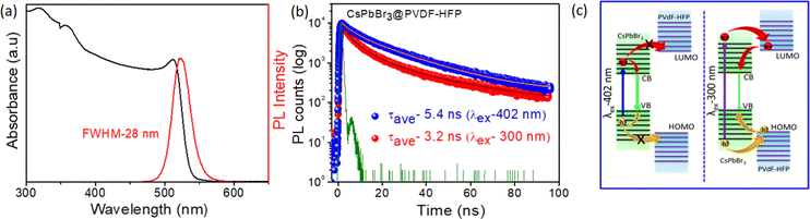 |
| | Fig. 6 (a) Optical absorption and PL spectra of CsPbBr3@PVDF-HFP fiber; the sample was excited at 420 nm, (b) time-correlated single photon counting (TCSPC) study of CsPbBr3@PVDF-HFP fiber after exciting the sample at 402 and 300 nm and monitoring the emission at 524 nm (laser pulse (IRF) green line), and (c) schematic representation of the charge-transfer mechanism under 402 (left panel) and 300 nm (right panel) excitation for the CsPbBr3@PVDF-HFP fiber. | |
Water stability study
To quantify their water stability, the synthesized electrospun CsPbBr3@PVDF-HFP fibers were immersed in water and the corresponding PL and FWHM were recorded for a fresh sample and after the 10th day. During this period, we noticed there was no appreciable PL change or change in FWHM (Fig. S5, ESI†) in the CsPbBr3@PVDF-HFP fibers. In addition, the electrospun CsPbBr3@PVDF-HFP fibers retained 90% of PLQY after 10 days of storage. This result clearly showed the high stability of CsPbBr3 after the encapsulation with the PVDF-HFP fiber, where the PVDF-HFP provided good stability for CsPbBr3 under water due to its hydrophobic characteristics.19
Ultrafast transient absorption studies
In the present investigation, ultrafast transient absorption (TA) spectroscopy was employed to follow the charge-carrier dynamics, including the carrier relaxation and carrier-transfer dynamics, after exciting both CsPbBr3 NCs and CsPbBr3@PVDF-HFP fiber samples with 420 nm and 300 nm pump pulses (FWHM ∼120 fs) and monitoring the transients in the visible region.
420 nm pump excitation.
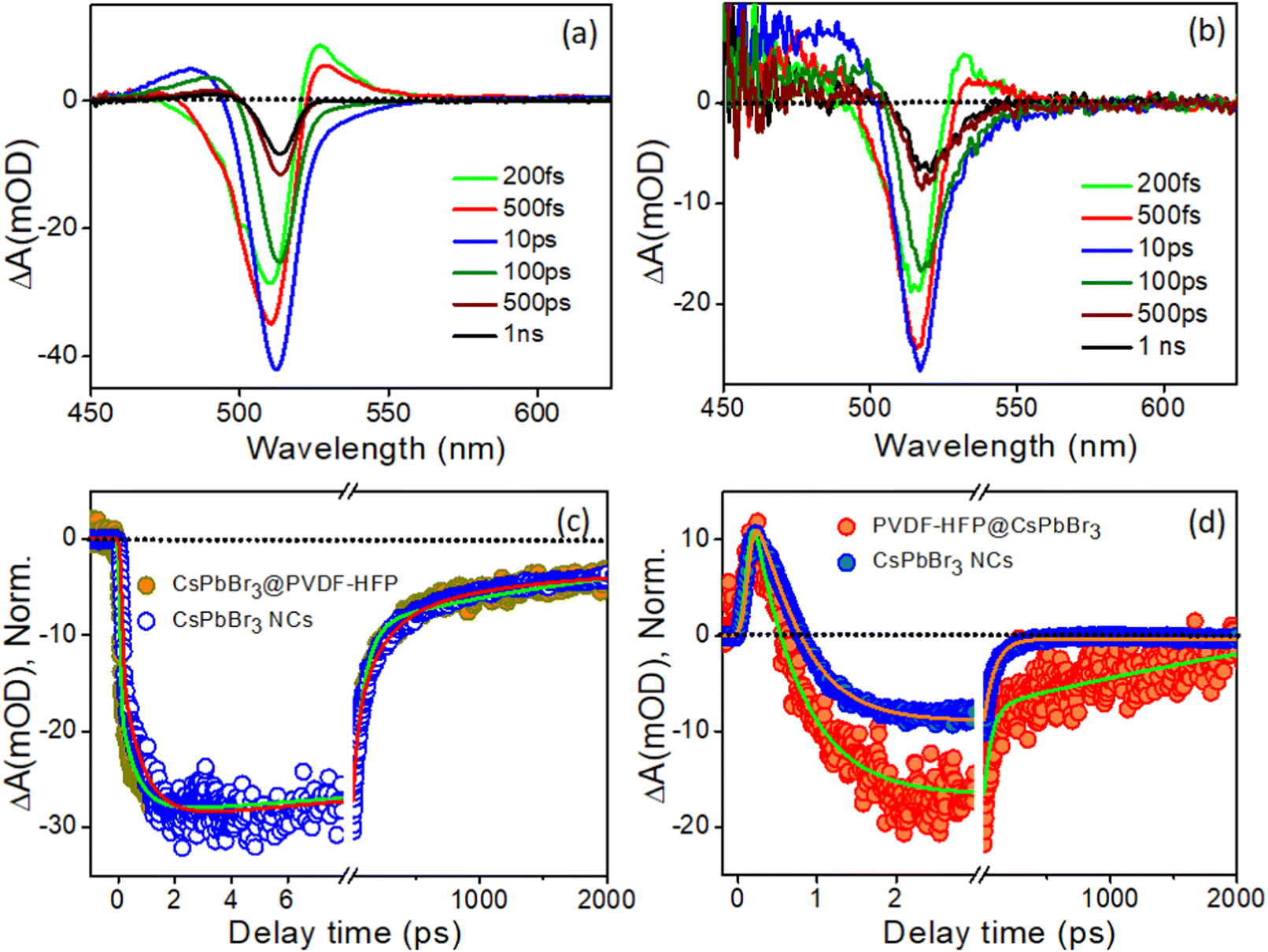
Fig. 7a and b depict the TA spectra at different time delays for CsPbBr3 NCs and CsPbBr3@PVDF-HFP fiber with the 420 nm pump pulse. Analogous features were observed in the CsPbBr3@PVDF-HFP fiber, including negative bleach and positive signals on either side of the bleach, corresponding to band edge exciton and photoinduced absorption, respectively.31,36–40 The ground state bleach was observed in the 490–525 nm spectral region, peaking at 517 nm. At the early time scale (0.2–0.5 ps), a positive absorption band could be discerned at 532 nm. Moreover, another positive absorption band was observed at 470–490 nm with a peak maximum at 488 nm, which could be attributed to the excited state absorption (ESA). In the TA spectrum, a negative absorption peak at 517 nm was ascribed to the ground state bleach due to state filling of the electronic states upon excitonic transition. The positive absorption below the band gap lying toward the higher wavelength side at around 532 nm was associated with probe-induced biexcitons formed as a consequence of the band renormalization due to the Stark effect, which is due to the carriers-induced electric field reducing the bandgap. Interestingly, the aforementioned TA spectra closely resembled the TA spectra of the bulk CsPbBr3 reported by our group and others.31,37,40
 |
| | Fig. 7 Time-dependent evolution of the transient absorption (TA) spectra of (a) CsPbBr3 NCs in toluene and (b) CsPbBr3@PVDF-HFP fiber at the excitation wavelength of 420 nm, (c) corresponding comparison of the bleaching and (d) biexciton kinetics of CsPbBr3@PVDF-HFP fibers after exciting the samples at 420 nm. | |
The transient kinetic traces were monitored at different wavelengths to explore the carrier dynamics of the synthesized CsPbBr3@PVDF-HFP fibers, and the results are depicted in Fig. 7c and d. The bleach kinetics at 517 nm fitted with a biexponential growth and multiexponential recovery with the time constants of τg1 = <150 fs and τg2 = 0.7 ps and τ1 = 72 ps, τ2 = 220 ps and τ3 = >1 ns, respectively. We observed a rise in the time of 0.7 ps for the bleaching of CsPbBr3@PVDF-HFP, which was in accordance with the cooling of the charge carriers to the band edge. Further, the multiexponential recovery kinetics could be ascribed to the charge recombination of the photoexcited charge carriers of CsPbBr3. Importantly, the growth and recovery kinetics exactly resembled those of CsPbBr3 NCs (Table S2, ESI†). Moreover, the probe induced biexciton signal was monitored at 532 nm. The formation time of the probe-induced biexciton signal could be fitted with a single exponential time component τg1 = <150 fs and the biexciton decay was found to be 250 fs (Table S3, ESI†). At 420 nm pump excitation, the charge carriers are confined within CsPbBr3, owing to the type-I band alignment. From the above results, it can be concluded that the CsPbBr3@PVDF-HFP fibers maintained the same charge-carrier dynamics as that of pristine CsPbBr3 NCs and did not undergo any charge (electron/hole)-transfer processes. This observation was the opposite to what we observed in our earlier report,31 where we explored the ultrafast charge-delocalization dynamics of CsPbBr3 NCs encapsulated in a transparent polystyrene (PS) fiber matrix. The CsPbBr3@PS displayed slower cooling compared to that of bare CsPbBr3 NCs, as delocalization of the carriers was possible even at 420 nm pump excitation.41,42
The CsPbBr3 exhibited conduction band (CB) and valence band (VB) positions (vs. vacuum) of −3.3 eV and −5.7 eV, respectively;43 on the other hand, PVDF-HFP is a well-known piezoelectric polymer with the highest occupied molecular orbital (HOMO) and lowest unoccupied molecular orbital (LUMO) as −6.13 eV and −2.45 eV, respectively.44,45 Interestingly, the PVDF-HFP (shell) did not induce any strain over CsPbBr3 (core) owing to the soft nature of the polymer. Owing to the high band offset of PVDF-HFP polymer, the carrier transfer and delocalization of the carriers from the CsPbBr3 to PVDF-HFP states could not be held liable. Herein, as the excitation wavelength was lower, i.e., 420 nm, it was not high enough to excite PVDF, which thus nullified the possibility of any kind of transfer process being involved. Also as previously observed by Mandal and co-workers, a high energy excitation enhances the transition probability of carriers.20 Exciting with photons having a higher energy than the band gap leads to the generation of electron–hole pairs, which in turn increases the photoconductivity of a material. So, to gain further insights into these processes, we employed TA spectroscopy for CsPbBr3@PVDF-HFP fibers under 300 nm excitation, so that the carriers were excited in both CsPbBr3 and PVDF-HFP.20
300 nm pump excitation.
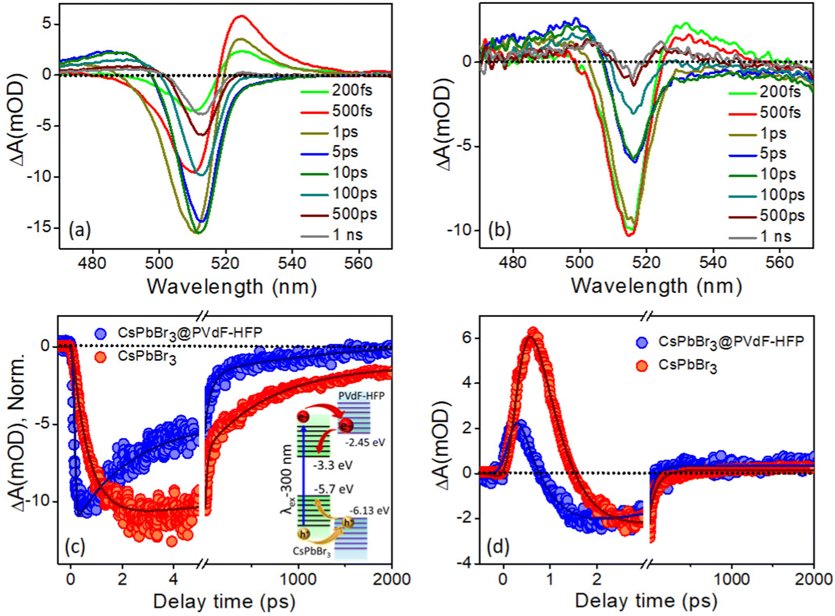
With the same intent of gaining insights into the carrier cooling and charge-transfer dynamics of CsPbBr3@PVDF-HFP fiber, we carried out a TA study at 300 nm pump excitation. Fig. 8a and b depict the TA spectra of the photoexcited bare CsPbBr3 NCs and CsPbBr3@PVDF-HFP fiber at different time delays. In the TA spectra, bleaching, biexciton, and PIA were noticed at 517, 526, and 488 nm, respectively.36–40 Due to the contribution of the high energy states under 300 nm pump excitation, the ground state 1S bleaching appeared to be broad compared to that of the 420 nm pump in both the samples.36 Further, to understand the exciton dynamics of the synthesized samples, transient kinetics were monitored at the bleaching position. The bleach kinetics of the bare CsPbBr3 NCs at 514 nm could be fitted to a biexponential growth with time constants of τg1 = 150 fs and τg2 = 1.2 ps and a multiexponential recovery with time constants of τ1 = 5.8 ps, τ2 = 52.7 ps and τ3 = 300 ps and τ4 = >1 ns. Interestingly, the bleach kinetics of CsPbBr3@PVDF-HFP fiber at 517 nm could be fitted with a very fast single exponential pulse width limited growth (<150 fs) and multiexponential recovery with time constants of τ1 = 2.2 ps, τ2 = 43.7 ps, τ3 = 250 ps and τ4 = >1 ns (Table S4, ESI†). Interestingly, compared to that of bare CsPbBr3 NCs, the growth and recovery were faster in the case of the CsPbBr3@PVDF-HFP fiber (Fig. 8c). The following reason may account for the fast growth and recovery in the CsPbBr3@PVDF-HFP fiber.20,21 In the case of 300 nm (4.1 eV) excitation, the charge carriers are excited across the band gap for both CsPbBr3 (2.4 eV) and PVDF-HFP (3.84 eV). The immediate outcome is that the majority of the carriers instead of cooling toward the band edge of CsPbBr3 delocalize among CsPbBr3 and PVDF-HFP energy states and some of them are lost as an outcome of trapping at the interface. This was reflected in the faster growth as well as recovery seen for the CsPbBr3@PVDF-HFP sample (inset: Fig. 8c). The kinetics for the bare CsPbBr3 NCs was fitted biexponentially, while for CsPbBr3@PVDF-HFP, the growth fitted CsPbBr3@PVDF-HFP alone, which indicated an underlying transfer mechanism took place. This was not the case under 420 nm excitation, where only the CsPbBr3 NCs were photoexcited, since the excitation energy (2.95 eV) was insufficient to create photogenerated charge carriers across the single exponential case (IRF limited growth). This led to faster cooling in PVDF (whose band gap was much higher, 3.84 eV). So, the resultant kinetics for both the CsPbBbr3 NCs and CsPbBr3@PVDF-HFP samples were similar.
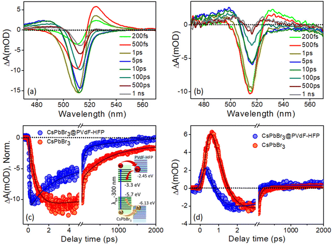 |
| | Fig. 8 Time-dependent evolution of the transient absorption (TA) spectra for: (a) control experiment using the CsPbBr3 NCs in toluene and (b) CsPbBr3@PVDF-HFP fiber at the excitation wavelength of 300 nm. Comparison of (c) bleaching (inset: plausible mechanism of charge transfer from CsPbBr3 to PVDF-HFP states) and (d) biexciton kinetics of CsPbBr3@PVDF-HFP fiber after exciting the samples at 300 nm and monitoring the kinetics were at the peak maxima. | |
To further understand the charge-carrier mechanism of CsPbBr3@PVDF-HFP, the biexciton dynamics were investigated. The probe-induced biexciton signal was monitored at 524 and 528 nm for CsPbBr3 NCs and CsPbBr3@PVDF-HFP (Fig. 8d) respectively. The observed TA kinetics of biexciton growth and the recovery looked very different for CsPbBr3@PVDF-HFP compared to those of CsPbBr3 NCs. Fig. 8d depicts the biexciton kinetics of CsPbBr3 NCs at 524 nm, which could be fitted with a growth time of 200 fs and decay time of 410 fs along with single exciton growth, followed by a multiexponential recovery (Table S5, ESI†). More importantly, with the same 300 nm pump, the biexciton growth kinetics for CsPbBr3@PVDF-HFP could be fitted with a time constant of <150 fs along with a decay time constant of 250 fs. It was interesting to see that the biexciton growth and decay of CsPbBr3@PVDF-HFP were much faster compared to those of CsPbBr3 NCs at 300 nm excitation. Upon photoexcitation, biexcitons generated in CsPbBr3@PVDF-HFP fibers become dissociated due to delocalization of charge carriers within CsPbBr3 and PVDF-HFP energy states. The TA studies clearly indicated that far band edge excitation leads to efficient charge transfer from CsPbBr3 to PVDF-HFP. Thus, upon far band gap pump excitation, the conductivity of the composite material concurrently increased, which was not the case with 420 nm pump excitation.
Low-temperature transient absorption study
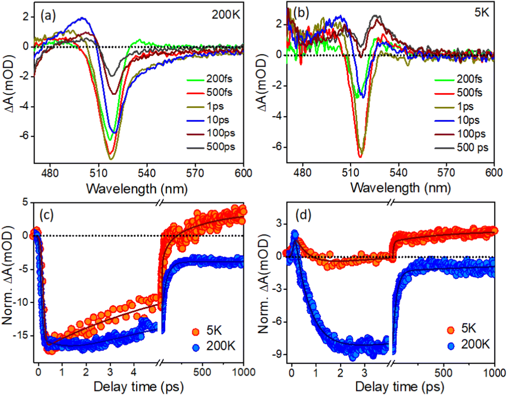
It was noticed that there are only a limited number of reports available in literature on low-temperature TA studies of CsPbBr3 NCs. Consequently, there is no report available in the literature regarding the low-temperature transient study of in situ-formed CsPbBr3 inside PVDF-HFP electrospun fibers. Yet, it is important to understand the carrier dynamics of CsPbBr3@PVDF-HFP fibers at cryogenic temperatures to develop highly efficient opto-electronic devices, which may be subjected to such low temperatures while under operational conditions. Here, CsPbBr3@PVDF-HFP was excited with a 420 nm pump and the dynamics were monitored in a wide temperature range from 300 K down to 5 K (here, we present the TA data for 200 K down to 5 K and as the TA data at 300 K is already given in Fig. 7, so, we omitted the TA of 300 K in order to avoid repetition of the data). Fig. 9a,b and Fig. S4a (ESI†) depict the temperature-dependent TA spectra of CsPbBr3@PVDF-HFP fiber deposited over glass (sample preparation is given in the ESI†) at a wide range of temperatures from 200 K down to 5 K excited (λex) at 420 nm. At the early time scale in all the spectral (5 K to 200 K) responses, we noticed three obvious spectral features, as also observed in the room temperature studies conducted for the dispersed samples, namely the ground-state photobleaching (GSB) peak at 514–518 nm in the position of the band edge and photoinduced absorptions (PIA) on either side. The PIA signal at the low energy side coming from the biexcitons completely vanished after 0.5 ps and the TA signal was completely dominated by the GSB at later time scales (200 K). Moreover, we found that the 1S excitonic position of the CsPbBr3@PVDF-HFP fiber was continuously shifted toward lower energy upon decreasing the temperatures from 300 K to 5 K (514–518 nm), due to the decrement in the band gap.36,37,46–52 It is clear that the CsPbBr3@PVDF-HFP fiber synthesized by the in situ electrospinning method resulted in the formation of surface trap states stemming from Br vacancies.39 From the TA studies through the vast ranges of temperature, it was clearly observed that the CsPbBr3@PVDF-HFP fibers were prone to forming defects owing to their larger size. Further, we monitored the temperature-dependent carrier cooling kinetics near the spectral maxima and these are depicted in Fig. 9c. Interestingly, the carrier cooling of CsPbBr3@PVDF-HFP fibers was much faster (0.21 ps) at 5 K compared to that of 0.62 ps at 200 K. The growth kinetics was faster in the case of 5 K and became slower upon increasing the temperature to 300 K (Table S6, ESI†). The faster cooling at 5 K was a consequence of the quicker relaxation of the charge carriers to the band edge because the lattice was completely frozen at 5 K, which leads to an absence of carrier–longitudinal (LO) phonon coupling. Thus, at 5 K, the carrier relaxation is mediated by acoustic phonons and there is no possibility of polaron formation, which could otherwise interfere in the carrier-cooling process.38,51Fig. 9d and Fig. S4c show the biexciton kinetics monitored in the peak maxima over a wide range of temperatures (200–5 K). The CsPbBr3@PVDF-HFP fiber exhibited τ1 = <100 fs biexciton growth for all the temperatures at 420 nm excitation. However, biexciton decays were slower (320 fs) at 5 K compared to that of 240 fs at 200 K. Upon decreasing the temperature from 200 to 5 K, the kinetics was observed to become positive at long time scales at the position of both the bleaching and biexciton maxima, which might be due to the trapping of charge carriers in the CsPbBr3@PVDF-HFP fiber, as the CsPbBr3@PVDF-HFP fibers are more prone to defects (Table S7, ESI†). From the above observation, it can be concluded that CsPbBr3@PVDF-HFP fibers can be effectively used for high-performance optoelectronic as well as photovoltaic applications.52
 |
| | Fig. 9 (a and b) TA spectra of CsPbBr3@PVDF-HFP fiber with the temperature of 200 and 5 K under 420 nm pump excitation and (c and d) bleach and biexciton kinetics at different temperature for CsPbBr3@PVDF-HFP fiber monitored at 514 and 530 nm probe wavelength respectively. | |
Conclusions
In summary, we successfully synthesized CsPbBr3@PVDF-HFP fibers using a facile one-step electrospinning method. The in situ synthesis of CsPbBr3 inside the PVDF-HFP fibers induced the electroactive β-phase, which efficiently avoided the cost-efficient, time-consuming, and tedious methods commonly used for polar phase formation in PVDF-HFP. The structural and optical studies suggested that the crystallinity and strong light absorption properties were maintained even after CsPbBr3 formation inside the fiber matrix. TRPL studies witnessed efficient charge transfer from CsPbBr3 to PVDF-HFP at 300 nm over that of 402 nm excitation in the fiber matrix. Furthermore, the aforementioned claims were confirmed through femtosecond TA spectroscopy. The excitation-dependent transient absorption study evidently showed that upon far band edge excitation of both CsPbBr3 and PVDF-HFP, an efficient delocalization of the carriers takes place, which would lead to an increase in the photoconductivity; whereas, there was no possibility of such carrier transfer at low pump excitation energies. The TA studies verified the formation of stable CsPbBr3@PVDF-HFP fibers through evidence of all its optical properties being similar to those of CsPbBr3 NCs, even at cryogenic temperatures. Importantly, the engineering of electroactive polymers with CsPbBr3 may efficiently be utilized for next-generation piezoelectric-based energy-harvesting applications. This comprehensive study provides a number of photophysical insights and would pave the way for the development of flexible and highly efficient solar cells and photodetector devices.
Author contributions
The manuscript was written through contributions of all the authors. All authors have given approval to the final version of the manuscript.
Conflicts of interest
There are no conflicts to declare.
Acknowledgements
K. J. B. thank SERB-NPDF (PDF/2019/000549), India for his National Postdoctoral research fellowship. G. K., A. S., H. B., and N. G. thank INST, Mohali for their research fellowships. H. N. G. thank DST India for the project SERB/DST (CRG/2019/000938). A. K. thank Department of Science and Technology (DST) for Inspire Research fellowship (IF-180009) and H. N. G. is grateful to DST, Govt. of India, for JC Bose fellowship (JCB/2018/000047) and the DST project Sanction No. SERB/DST (CRG/2019/000938). The authors acknowledge Institute of Nano Science and Technology, Mohali for providing instrument facilities for supporting this research work.
References
- M. V. Kovalenko, L. Protesescu and M. I. Bodnarchuk, Science, 2017, 358, 745–750 CrossRef CAS PubMed.
- L. Protesescu, S. Yakunin, M. I. Bodnarchuk, F. Krieg, R. Caputo, C. H. Hendon, R. X. Yang, A. Walsh and M. V. Kovalenko, Nano Lett., 2015, 15, 3692–3696 CrossRef CAS PubMed.
- Q. A. Akkerman, G. Raino, M. V. Kovalenko and L. Manna, Nat. Mater., 2018, 17, 394–405 CrossRef CAS PubMed.
- X. Li, D. Yu, F. Cao, Y. Gu, Y. Wei, Y. Wu, J. Song and H. Zeng, Adv. Funct. Mater., 2016, 26, 5903–5912 CrossRef CAS.
- T. A. Berhe, W. N. Su, C. H. Chen, C. J. Pan, J. H. Cheng, H. M. Chen, M. C. Tsai, L. Y. Chen, A. A. Dubale and B. J. Hwang, Energy Environ. Sci., 2016, 9, 323–356 RSC.
- H. Guan, S. Zhao, H. Wang, D. Yan, M. Wang and Z. Zang, Nano Energy, 2020, 67, 104279 CrossRef CAS.
- Q. Mo, C. Chen, W. Cai, S. Zhao, D. Yan and Z. Zang, Laser Photonics Rev., 2021, 15, 2100278 CrossRef CAS.
- X. Li, W. Cai, H. Guan, S. Zhao, S. Cao, C. Chen, M. Liu and Z. Zang, Chem. Eng. J., 2021, 419, 129551 CrossRef CAS.
- B. Wang, J. Peng, X. Yang, W. Cai, H. Xiao, S. Zhao, Q. Lin and Z. Zang, Laser Photonics Rev., 2022, 2100736 CrossRef CAS.
- S. Peng, G. Jin, L. Li, K. Li, M. Srinivasan, S. Ramakrishna and J. Chen, Chem. Soc. Rev., 2016, 45, 1225–1241 RSC.
- J. Hai, H. Li, Y. Zhao, F. Chen, Y. Peng and B. Wang, Chem. Commun., 2017, 53, 5400–5403 RSC.
- Y. Wang, Y. Zhu, J. Huang, J. Cai, J. Zhu, X. Yang, J. Shen and C. Li, Nanoscale Horiz., 2017, 2, 225–232 RSC.
- Y. Wang, Y. Zhu, J. Huang, J. Cai, J. Zhu, X. Yang and C. Li, J. Phys. Chem. Lett., 2016, 7, 4253–4258 CrossRef CAS PubMed.
- V. K. Thakur and R. K. Gupta, Chem. Rev., 2016, 116, 4260–4317 CrossRef PubMed.
- J. Chang, M. Dommer, C. Chang and L. Lin, Nano Energy, 2012, 1, 356–371 CrossRef CAS.
- A. Gebrekrstos, G. Madras and S. Bose, Cryst. Growth Des., 2019, 19, 5441–5456 CrossRef CAS.
- B. Mohammadi, A. A. Yousefi and S. M. Bellah, Polym. Test., 2007, 26, 42–50 CrossRef CAS.
- F. Wang, H. Wang, A. Ali, Y. Zhang, X. Cui and Y. Liu, Inorg. Chem. Commun., 2019, 106, 99–103 CrossRef CAS.
- P. Liang, P. Zhang, A. Pan, K. Yan, Y. Zhu, M. Yang and L. He, ACS Appl. Mater. Interfaces, 2019, 11, 22786–22793 CrossRef CAS PubMed.
- A. Sultana, P. Sadhukhan, M. M. Alam, S. Das, T. R. Middya and D. Mandal, ACS Appl. Mater. Interfaces, 2018, 10, 4121–4130 CrossRef CAS PubMed.
- A. Sultana, M. M. Alam, P. Sadhukhan, U. K. Ghorai, S. Das, T. R. Middya and D. Mandal, Nano Energy, 2018, 49, 380–392 CrossRef CAS.
- S. Zhang, Y. Lu, B. Lin, Y. Zhu, K. Zhang, N. Y. Yuan, J. N. Ding and B. Fang, Sol. Energy Mater. Sol. Cells, 2017, 170, 178–186 CrossRef CAS.
- T. Dong, J. Zhao, G. Li, F. C. Li, Q. Li and S. Chen, ACS Appl. Mater. Interfaces, 2021, 13, 39748–39754 CrossRef CAS PubMed.
- R. Cheng, Z. B. Liang, L. Zhu, H. Li, Y. Zhang, C. F. Wang and S. Chen, Angew. Chem., Int. Ed., 2022, e202204371 CAS.
- G. C. Dadol, A. Kilic, L. D. Tijing, K. J. A. Lim, L. K. Cabatingan, N. P. B. Tan, E. Stojanovska and Y. Polat, Mater. Today Commun., 2020, 25, 101656 CrossRef CAS.
- S. Maiti, J. Dana and H. N. Ghosh, Chem. – Eur. J., 2019, 25, 692–702 CrossRef CAS PubMed.
- P. Singhal and H. N. Ghosh, J. Phys. Chem. C, 2018, 122, 17586–17600 CrossRef CAS.
- R. Aepuru, S. Mondal, N. Ghorai, V. Kumar, H. S. Panda and H. N. Ghosh, J. Phys. Chem. C, 2018, 122, 27273–27283 CrossRef CAS.
- S. Mondal, T. Paul, S. Maiti, B. K. Das and K. K. Chattopadhyay, Nano Energy, 2020, 74, 104870 CrossRef CAS.
- N. Senthilkumar, K. J. Babu, G. G. Kumar, A. R. Kim and D. J. Yoo, Ind. Eng. Chem. Res., 2014, 53, 10347–10357 CrossRef CAS.
- K. J. Babu, G. Kaur, L. Biswal, G. De and H. N. Ghosh, Chem. – Eur. J., 2021, 27, 683–691 CrossRef CAS PubMed.
- D. Yuan, Z. Li, W. Thitsartarn, X. Fan, J. Sun, H. Li and C. He, J. Mater. Chem. C, 2015, 3, 3708–3713 RSC.
- Q.-F. Li, J.-T. Wang, B. Tian, S. Kong and T. Z. Wang, Eur. J. Inorg. Chem., 2018, 4215–4220 CrossRef CAS.
- M. Ou, W. Tu, S. Yin, W. Xing, S. Wu, H. Wang, S. Wan, Q. Zhong and R. Xu, Angew. Chem., Int. Ed., 2018, 57, 13570–13574 CrossRef CAS PubMed.
- C. C. Ilie, F. Guzman, B. L. Swanson, I. R. Evans, P. S. Costa, J. D. Teeter, M. Shekhirev, N. Benker, S. Sikich, A. Enbabders, P. A. Dowben, A. Sinitskii and A. J. Yost, J. Phys.: Condens. Matter, 2018, 30, 18LT02 CrossRef CAS PubMed.
- G. Kaur, K. J. Babu, N. Ghorai, T. Goswami, S. Maiti and H. N. Ghosh, J. Phys. Chem. Lett., 2019, 10, 5302–5311 CrossRef CAS PubMed.
- A. Shukla, G. Kaur, K. J. Babu, N. Ghorai, T. Goswami, A. Kaur and H. N. Ghosh, J. Phys. Chem. Lett., 2020, 11, 6344–6352 CrossRef CAS PubMed.
- G. Kaur, K. J. Babu and H. N. Ghosh, J. Phys. Chem. Lett., 2020, 11, 6206–6213 CrossRef CAS PubMed.
- K. J. Babu, G. Kaur, A. Shukla, A. Kaur, T. Goswami, N. Ghorai and H. N. Ghosh, J. Phys. Chem. Lett., 2020, 12, 302–309 CrossRef PubMed.
- H. Chung, S. I. Jung, H. J. Kim, W. Cha, E. Sim, D. Kim, W.-K. Koh and J. Kim, Angew. Chem., Int. Ed., 2017, 56, 4160–4164 CrossRef CAS PubMed.
- S. L. Sewall, A. Franceschetti, R. R. Cooney, A. Zunger and P. Kambhampati, Phys. Rev. B: Condens. Matter Mater. Phys., 2009, 80, 81310 CrossRef.
- A. M. Smith, A. M. Mohs and S. Nie, Nat. Nanotechnol., 2009, 4, 56–63 CrossRef CAS PubMed.
- S. Maiti, T. Debnath, P. Maity and H. N. Ghosh, J. Phys. Chem. C, 2015, 119, 8410–8416 CrossRef CAS.
- P. Maity, J. Dana and H. N. Ghosh, J. Phys. Chem. C, 2016, 120, 18348–18354 CrossRef CAS.
- K. A. Bogdanowicz, D. Augustowski, J. Dziedzic, P. Kwaśnicki, W. Malej and A. Iwan, Materials, 2020, 13, 2721 CrossRef CAS PubMed.
- B. T. Diroll, H. Zhou and R. D. Schaller, Adv. Funct. Mater., 2018, 28, 1800945 CrossRef.
- A. Dey, P. Rathod and D. Kabra, Adv. Opt. Mater., 2018, 6, 1800109 CrossRef.
- B. T. Diroll, G. Nedelcu, M. V. Kovalenko and R. D. Schaller, Adv. Funct. Mater., 2017, 27, 1606750 CrossRef.
- H. Ryu, H. R. Byun, K. M. McCall, D. Y. Park, T. J. Kim, S. Jeong, M. G. Kanatzidis and J. I. Jang, J. Am. Chem. Soc., 2021, 143, 2340–2347 CrossRef CAS PubMed.
- A. Dey, J. Ye, A. De, E. Debroye, S. K. Ha, E. Bladt, A. S. Kshirsagar, Z. Wang, J. Yin, Y. Wang and L. N. Quan,
et al.
, ACS Nano, 2021, 15, 10775–10981 CrossRef CAS PubMed.
- K. Justice Babu, G. Kaur, A. Shukla, R. Saha, A. Kaur, M. S. Deva, D. K. Yadav and H. N. Ghosh, ACS Photonics, 2022, 9, 969–978 CrossRef CAS.
- K. Maity, U. Pal, H. K. Mishra, P. Maji, P. Sadhukhan, Z. Mallick, S. Das, B. Mondal and D. Mandal, Nano Energy, 2022, 92, 106743 CrossRef CAS.
Footnotes |
| † Electronic supplementary information (ESI) available: Experimental details, instrumentation details, optical studies, EDS analysis, quantum yield measurement, low temperature TA spectra, kinetics and tables. See DOI: https://doi.org/10.1039/d2ma00503d |
| ‡ Present address: S. N. Bose National Centre for Basic Sciences, Salt Lake, Kolkata 700106, India. |
|
| This journal is © The Royal Society of Chemistry 2022 |
Click here to see how this site uses Cookies. View our privacy policy here. 
 Open Access Article
 This Open Access Article is licensed under a Creative Commons Attribution-Non Commercial 3.0 Unported Licence
 a,
Goutam
De‡
a,
Goutam
De‡