
 Open Access Article
 This Open Access Article is licensed under a
 Creative Commons Attribution 3.0 Unported Licence
Morphological evolution driven semiconducting nanostructures for emerging solar, biological and nanogenerator applications
Avanish Kumar
Srivastava
ab,
Jai Shankar
Tawale
c,
Rajni
Verma
 d,
Daksh
Agarwal
ef,
Charu
Sharma
ab,
Ashavani
Kumar
g and
Manoj Kumar
Gupta
*ab
d,
Daksh
Agarwal
ef,
Charu
Sharma
ab,
Ashavani
Kumar
g and
Manoj Kumar
Gupta
*ab
aCSIR-Advanced Materials and Processes Research Institute, Bhopal, Madhya Pradesh 462026, India. E-mail: mkgupta@ampri.res.in; Fax: +91 755-2457042; Tel: +91 9977360351
bAcademy of Scientific and Innovative Research (AcSIR), Ghaziabad-201002, India
cCSIR-National Physical Laboratory, New Delhi-110012, India
dSchool of Physics, The University of Melbourne, Parkville, Victoria 3010, Australia
eDepartment of Materials Science and Engineering, University of Pennsylvania, Philadelphia, PA 19104, USA
fLam Research Corporation, Fremont, CA 94538, USA
gDepartment of Physics, National Institute of Technology Kurukshetra, Haryana, 136119, India
First published on 3rd October 2022
Abstract
Metal oxide nanostructures are extremely fascinating smart and functional materials owing to their outstanding wide and tunable band gap, biocompatibility, high electrochemical coupling coefficient, high photostability, high sensitivity, non-toxicity, high electron mobility and high thermal/chemical stability properties. The morphologies of the metal oxide nanostructures are highly influenced by growth parameters and methods. The performance of solar cell/sensors, biological, electronic and energy harvesting properties are highly varied with the morphological changes in the nanostructures. The progress of the metal oxide nanostructures for particular applications has been discussed in many earlier review articles; however, a comprehensive review article based on the various morphologies of metal oxide nanostructures (especially, together with ZnO and SnO2) for their numerous and next-generation applications has not been reported yet. The present review article summarizes the recent progresses and applications of ZnO and SnO2 nanostructures to provide a comprehensive understanding of the effect of morphologies on the performance of the technological devices and biosensors. The growth of various nanostructures (such as tetrapods, nanorods and nanowires) and their wide applications in solar cells, biological field, sensors and piezoelectric nanogenerators/piezotronics are covered in the present review. This review also provides a detailed comparison of the performances of ZnO nanostructure-based solar cells with SnO2-based solar cells and flexible devices. The performance of the solar cell in terms of morphology, electron mobility, band gap and piezoelectric properties are also discussed. This paper also gives insights into the antimicrobial, antilarvicidal and anticancer activities of various ZnO and SnO2 nanostructures. In addition, special deliberation has been made on the fabrication of novel piezoelectric nanogenerators based on the various morphologies of ZnO (such as nanowires, nanosheets and nanorods) for scavenging mechanical energy from the living environment. Finally, the benefits, challenges and future outlook of metal oxide nanostructures for their potential application in opto-electronic, sensors, biomedical energy harvesting and next-generation flexible self-powered nanosystems are highlighted.
 Avanish Kumar Srivastava | Dr Avanish Kumar Srivastava received his Master's degree from IIT Roorkee, MTech from IIT Kanpur, and doctorate from IISc, Bangalore, India in metallurgy science. He is presently working as the Director at CSIR-Advanced Materials and Processes Research Institute (CSIR-AMPRI) Bhopal, Madhya Pradesh, India and Director (Additional Charge) CSIR-National Metallurgical Laboratory Jamshedpur Jharkhand, India. He has expertise in the growth of semiconducting, metal oxide and perovskite nanomaterials materials, and their characterization and evaluation of various properties through electron microscopes. He is President of the Electron Microscope Society of India. He has authored more than 350 international articles. He recieved various awards including NMD-2011 and NRDC-2020. |
 Jai Shankar Tawale | Dr Jai Shankar Tawale received his PhD degree in Physics from the National Institute of Technology (NIT) Kurukshetra, Haryana. He is currently working in the Indian Reference Materials Division (BND) at CSIR-National Physical Laboratory, New Delhi. His current research interest includes oxide nanomaterials and their composites, reference materials, and characterization of nanomaterials, and has published more than 35 research articles. |
 Rajni Verma | Dr Rajni Verma received her PhD in 2018 from the CSIR-National Physical Laboratory, India, for her research on the synthesis and applications of various nanomaterials. As a postdoctoral researcher, she worked at the Indian Institute of Technology Delhi in metal organic frameworks for photocatalytic applications. After that, she was awarded a prestigious McKenzie Fellowship in 2019, and her research interest is currently focused on the nano-bio interface at the School of Physics, The University of Melbourne, Australia. |
 Daksh Agarwal | Dr Daksh Agarwal is presently working at the Technology Development group at Lam Research, USA. He obtained a PhD degree from the University of Pennsylvania in Material Science and Engineering in 2016. His current research interest includes oxide nanomaterials, and their application in energy and sensors. He has more than 20 research articles in reputed journals. |
 Charu Sharma | Ms Charu Sharma received her Bachelor in Science (BSc) degree from Regional Institute of Education, Ajmer (India) and Masters degree in Applied Physics from Babasaheb Bhimrao Ambedkar University, Lucknow (India). She is a Gold Medalist. Currently, she is pursuing a PhD under the supervision of Dr Manoj Kumar Gupta and Dr Avanish Kumar Srivastava from the Academy of Scientific and Innovative Research-Advanced Materials and Processes Research Institute (AcSIR-AMPRI), Bhopal (India). Her research interest is mainly focused on the synthesis of two-dimensional nanomaterials and its application as a piezoelectric energy harvester. |
 Ashavani Kumar | Dr Ashavani Kumar is Professor & Head, Department of Physics, National Institute of Technology Kurukshetra, India. He received a PhD degree in Physics (1994) from Aligarh Muslim University, Aligarh, India. He has been in academics, research and administration for over 30 years. His research activities cover high-energy physics, instrumentation, materials engineering and nanotechnology for various applications. He has published more than 100 research papers in international reputed journals and contributed more than 200 papers in proceedings. Dr Kumar was awarded the International Postdoctoral Fellowship in Experimental Physics (OPEN) by the National Institute for Nuclear Physics (INFN-Fellowships), Govt. of Italy. Dr Kumar also has other administrative responsibilities in the institute. |
 Manoj Kumar Gupta | Dr Manoj Kumar Gupta received his PhD degree from the University of Delhi, India, in 2011. Presently, he is working as a Scientist at CSIR-Advanced Materials and Processes Research Institute (CSIR-AMPRI) Bhopal. He was awarded the CSIR-Young Scientist Award in Physical Science (Including Instrumentation) and CSIR Raman Research Fellowship. He also holds a DST-INSPIRE Faculty fellowship. He worked as a postdoctoral fellow at Sungkyunkwan University, South Korea from 2014 to 2017. He has visited various countries and given various scientific talks in USA, China and Finland. His current research areas are nano-materials synthesis and fabrication of energy harvesting nanodevices, such as piezoelectric, pyroelectric, triboelectric and hybrid nanogenerators and polymer composites. He has more than 60 international publications in reputed journals and has five international patents. |
1. Introduction
Presently, the emerging field of nanoscience, nanoengineering, nanoelectronics and nanomaterials has played a significant commercial and social impact towards solutions for energy, sensor, health and environmental concerns.1,2 In recent years, metal oxide nanomaterials have received much attention because of their outstanding structural, electrical and optical properties, which made them attractive materials for numerous potential applications in several sectors, such as optics, energy, electronics, dielectric, biomedical and photonics.2 Metal oxide nanostructures in a wide number of morphologies (such as nanobelts, nanoflowers, nanotubes, nanorings, and nanowires) have been synthesized and reported by various authors worldwide.2,3 To understand the fundamental phenomena in low-dimensional systems and to develop the next-generation nanodevices for solar, sensor, energy and biomedical applications with high performance, the synthesis of metal oxide nanostructures is highly beneficial. The nanomaterials are distinguished on the basis of their size and they are synthesized by various novel synthesis approaches, where a reduced dimension at the nanoscale can alter or enhance their physical, chemical and electronic properties, which are the basis of science and nanotechnology.1–5 The nanomaterials are broadly classified on the basis of dimensionality, origin and needs of the 21st century for a variety of societal applications. The uniform size distribution in nano-structural materials along with size and morphology play an important role in controlling the optical and sensing properties, which have decisive roles in future nanotechnology, for manufacturing smart and efficient devices.6–14 A structure that has confinement in all three dimensions (x, y, z) at the nanoscale is called a 0 (zero)-D structure. The nanoparticles or quantum dots (including single crystalline, polycrystal nature and amorphous) with various morphologies of discs, sheets, cubes and platelets reveal quantum confinement in all three dimension to some extent.15 Nanomaterials with single crystallinity are often known as nanocrystals. If all three dimensions of the nanocrystals are confined to the 1–10 nm scale, the crystal is termed as a quantum dot.16–25 Whiskers and fiber-like structures with diameters ranging from a few nanometers to several hundred nanometers are known as one-dimensional nanostructures. Thus, nanowires and nanorods are referred to as one-dimensional (1-D) nanostructures with diameter in the nanoscale range and length in few hundred nanometers. Morphologies, such as the nano-belt, tube, comb, needle and cables, are considered 1-D nanostructures. The nanorods are about 10![[thin space (1/6-em)]](https://www.rsc.org/images/entities/char_2009.gif) 000 times smaller than the human hair and are packed together in such a way that light particles cannot pass through them, resulting in most of the light being absorbed.26–30 In addition, in 2D materials, one of the dimensions is nanoscale (confined in one direction only) and the other dimension varies in the micrometer scale. Thin film or layer structures deposited on various substrates of any composition and being crystalline/amorphous in nature are considered 2-D nanomaterials. Two-dimensional (2-D) nanostructures include plates, sheets, triangles, single and multilayer films and transparent coating type. Accordingly, graphene as one-atom thick plane sheet of carbon is the best example of a two-dimensional nanostructure. The 2D materials demonstrated various unique properties, such as excellent superconductivity, new electronic and physical properties, along with florescence properties. The anisotropic transport properties of the 2D materials hold promising applications in devices covering solar cells, UV sensors, touch screens, electronic gadgets and smart mobile phones. The 2-D nanostructures alone or combined with other materials as a composite have potential to play a leading role in incredible future technologies.31,32 In addition to that, polycrystals or bulk materials with three arbitrary dimensions of more than 100 nm size of nanosized crystals are three-dimensional (3-D) nanostructures. Among the various nanostructures, metal oxide nanostructures (including, ZnO and SnO/SnO2) have recently attracted huge interest due to their proven technological, medical and industrial applications.30–32Fig. 1 shows the schematic image of the application of the metal oxide nanostructures in numerous sectors, including automobile, optical, biological, sensors, solar and piezoelectric nanogenerators. In the present review, we specially cover the synthesis of various morphologies of the ZnO and SnO2-based nanostructure, and their sensing, solar, energy and biomedical applications are discussed. Moreover, the article provides a comprehensive review on the recent development in the synthesis, optical, humidity sensing and energy applications of ZnO and SnO2 nanostructures and their composites with polymers. A brief survey on the cost-effective and mixed synthesis approach to obtain several crystalline nanostructures with tunable morphological and properties is also included. Several metal oxide morphologies of ZnO and SnO2, such as nanorods, tetrapods, spherical, flower, octahedral shape geometry and their mixed counterpart with graphene layers for specific applications in future nanotechnology have been discussed. The effects of impurities, doping and composite nanostructures are also reviewed for new morphological designs based on metal oxide nanostructures to explore new directions in the field of advanced research in the forthcoming technologies. The fabrication of the flexible piezoelectric nanogenerator based on the ZnO and SnO2 nanostructures to convert mechanical vibrations from living environments is also discussed.
000 times smaller than the human hair and are packed together in such a way that light particles cannot pass through them, resulting in most of the light being absorbed.26–30 In addition, in 2D materials, one of the dimensions is nanoscale (confined in one direction only) and the other dimension varies in the micrometer scale. Thin film or layer structures deposited on various substrates of any composition and being crystalline/amorphous in nature are considered 2-D nanomaterials. Two-dimensional (2-D) nanostructures include plates, sheets, triangles, single and multilayer films and transparent coating type. Accordingly, graphene as one-atom thick plane sheet of carbon is the best example of a two-dimensional nanostructure. The 2D materials demonstrated various unique properties, such as excellent superconductivity, new electronic and physical properties, along with florescence properties. The anisotropic transport properties of the 2D materials hold promising applications in devices covering solar cells, UV sensors, touch screens, electronic gadgets and smart mobile phones. The 2-D nanostructures alone or combined with other materials as a composite have potential to play a leading role in incredible future technologies.31,32 In addition to that, polycrystals or bulk materials with three arbitrary dimensions of more than 100 nm size of nanosized crystals are three-dimensional (3-D) nanostructures. Among the various nanostructures, metal oxide nanostructures (including, ZnO and SnO/SnO2) have recently attracted huge interest due to their proven technological, medical and industrial applications.30–32Fig. 1 shows the schematic image of the application of the metal oxide nanostructures in numerous sectors, including automobile, optical, biological, sensors, solar and piezoelectric nanogenerators. In the present review, we specially cover the synthesis of various morphologies of the ZnO and SnO2-based nanostructure, and their sensing, solar, energy and biomedical applications are discussed. Moreover, the article provides a comprehensive review on the recent development in the synthesis, optical, humidity sensing and energy applications of ZnO and SnO2 nanostructures and their composites with polymers. A brief survey on the cost-effective and mixed synthesis approach to obtain several crystalline nanostructures with tunable morphological and properties is also included. Several metal oxide morphologies of ZnO and SnO2, such as nanorods, tetrapods, spherical, flower, octahedral shape geometry and their mixed counterpart with graphene layers for specific applications in future nanotechnology have been discussed. The effects of impurities, doping and composite nanostructures are also reviewed for new morphological designs based on metal oxide nanostructures to explore new directions in the field of advanced research in the forthcoming technologies. The fabrication of the flexible piezoelectric nanogenerator based on the ZnO and SnO2 nanostructures to convert mechanical vibrations from living environments is also discussed.
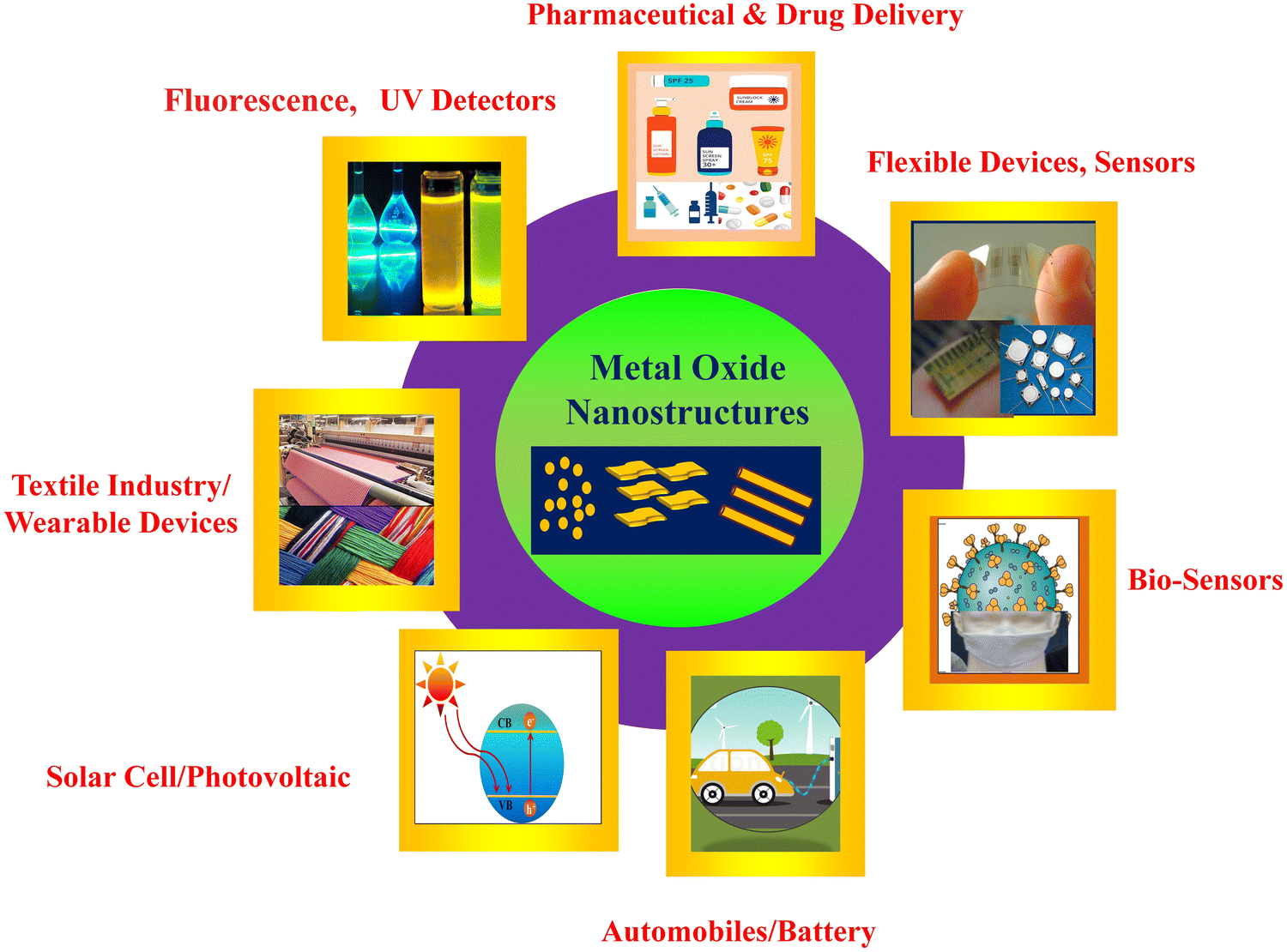 | ||
| Fig. 1 Various potential and industrial applications of metal oxide nanostructures. | ||
2. Synthesis of metal oxide nanostructures (ZnO and SnO2)
The preparation of nanostructure materials is one of the most important, challenging and crucial tasks for designing novel devices for specific applications. The synthesis of metal oxide nanomaterials with desired morphology and composition have stimulated great interest to fabricate efficient nano-devices for different applications. The morphological design includes various intriguing nanostructures, like particles, tubes, rods, needles, plate, sheet, ribbon, tetrapod, flower, octahedral and many other shapes. Controlling the growth formation and reproducibility of these nanostructures in terms of the uniform size distribution, identical in shape and elemental composition is an equally important and challenging task. Several growth techniques/methods have been reported to fabricate metal oxide nanostructure morphologies using top-down and bottom-up methods. In the bottom-up approach, molecular components arrange themselves into a more complex assembly atom-by-atom, molecule-by-molecule, and cluster-by-cluster from the bottom. Synthesis of nanoparticles by colloid dispersions is an example of the bottom-up approach. This approach is crucial and important to fabricating various dimensional nanostructures of small size and shape. The bottom-up approach offers a molecular-level and fabrication strategy that can be controlled for synthesis and nanoelectronic devices, which are not usually possible with top-down methods.33 In the top-down approach, nanosized structures or particles are prepared by breaking down the bulk material into nanoscale materials though various techniques.34 Moreover, recent hybrid nano manufacturing strategies that combine the advantages of both top-down and bottom-up approaches are being used for the large-scale and cost-effective generation of metal oxide nanostructures.35Various physical and chemical routes (such as thermal evaporation, laser ablation, hydrothermal route, template base synthesis, and sol–gel) have recently been employed to synthesize metal oxide nanostructures with the desired morphology for different properties and applications.36 This includes the example of the bottom up synthesis method, wherein the chemical routes are chosen to generate different nanostructures on a large scale and by controlling the growth parameters. The physical routes are more challenging, but a popular route to fabricate nanostructures at the large scale of the required structural morphology. Physical vapor deposition (PVD), which includes the condensation and evaporation of a material on a substrate in the form of a coating having a thickness in the nano-micro range, is an example of the top up approach. This method is also popular due to the high crystallinity and uniform quality of the nanomaterials. The thermal evaporation method is also used to achieve the metal oxide nanostructures due to its simple and economical properties. The thermal evaporation process involves sublimation of the source material at high temperature, and subsequent deposition of the vapor on certain substrates in a specific temperature region is used to achieve the required nanostructures. Recently, the flower-like ZnO nanorod was successfully developed by thermal evaporation without the use of any catalyst or template.37 The nano- and micron sizes of the ZnO with nanorod- and nanoparticle-like morphologies have been produced by the thermal evaporation method.38–40 The ZnO nanowires array was synthesized by thermal evaporation directly on a Zn foil.41 The ZnO tetrapods are also grown by the sublimation process by employing thermal evaporation to achieve optical properties and antibacterial applications.42–44 Moreover, the urchin-like morphology of the ZnO nanorods has also been reported by solution technique.43,44 Nanostructures with fascinating morphologies like the tetrapods and nanowires of ZnO have been successfully produced by the CVD method.44 Similarly, a cost-effective and simple thermal evaporation process was successfully employed to produce various morphologies of SnO2 nanostructures for optoelectronic, sensing and energy applications.45–54 The CVD-grown SnO2 nanostructures for optical and sensor applications have been also reported.45 The sol–gel approach is a well-known and popular process for the successful synthesis of various metal oxide nanomaterials.55 The sol–gel technique was widely used to fabricate dimensionally confined nanostructures of ZnO.56,57 The rich families of ZnO and SnO2 morphologies (including nanowires, nanotubes, nanorods and nanocrystals) were prepared by sol–gel method for various applications.58–63 The sol–gel method was also employed to produce bare and doped SnO2 nanostructures for many applications with enhanced performance.64–71 Moreover, the hydrothermal approach is widely used by researchers to obtain metal oxide nanostructures. These hydrothermally synthesized nanomaterials have been largely incorporated in composite nanomaterials to enhance the nanoscale materials properties. The ZnO and SnO2 nanostructures were successfully prepared by hydrothermal method for various morphologies and many nanoscale device properties. ZnO-reinforced polyaniline nanocomposite nanomaterials prepared by microwave-assisted hydrothermal synthesis for electrically conductive properties have also been reported.72 SnO2 backbone and ZnO nanostructures with hierarchical assembly by low-temperature hydrothermal synthesis approach have also been reported for optical applications.73–77
In addition, the combustion synthesis technique is a powerful route for the synthesis of nanostructures.77 The combustion method is a low-temperature, time-saving, energy efficient, self-propagating method, and involves a spontaneous exothermic redox reaction between a metal nitrate and organic fuel that is used to prepare nanomaterials. The method is based on the utilization of the heat energy produced during the exothermic spontaneous redox reaction between an oxidizer and reducing agent. The combustion method is emerging as a facile and economically viable technique, and was successfully used in the preparation of a large number of technologically useful oxides and nanomaterials.78–88 In addition to these novel synthesis methods, mixed strategies including physical and chemical routes are used to fabricate different nanomaterials. Currently, the hybrid synthesis is a popular approach to achieve the desired nanostructures through both chemical and physical efforts. The process is useful for the synthesis of composite nanostructures consisting of organic–inorganic hybrids. The incorporation of organic compounds into an inorganic matrix through either physical trapping or chemical bonding modifies various physical properties. However, the challenge is to prevent phase segregation of the nanomaterials. The intercalation process is recommended for the incorporation of guest species (atom, molecules and ions) in a layered crystalline host matrix, preserving the structural integrity of the host lattice.
2.1. ZnO nanostructure
In the last few decades, there has been growing importance of nanotechnology for high-end technological solutions. Furthermore, the study on the dimensional confinement of ZnO nanomaterials became a growing area in the nanotechnological advancement. ZnO is a popular piezoelectric, non-toxic and semiconducting metal oxide material with high electron mobility, large band gap and high diffusion coefficient. ZnO can be easily synthesized in several morphologies,including nanotubes, nanoflowers, nanorods, nanowires, nanocrystals and nanospheres.78 The ZnO nanostructure has been utilized for various ranges of applications, such as sensors, catalyst, solar cells, supercapacitors, surface coatings, biological, batteries, photodetectors and piezoelectric nanogenerators.ZnO exhibits wurtzite and zinc blende crystal structures. The wurtzite structure of ZnO is the most thermodynamically stable phase. ZnO has a hexagonal unit cell with the following lattice parameters: a = 0.324 and c = 0.520 nm (wurtzite). The ZnO structure can be understood as a cation (Zn2+) surrounded by four (O2−) anions at the corners of a tetrahedron (Fig. 2).89 ZnO is a key technological material, and the synthesis of the ZnO nanostructures has become a hot area of research due to its proven potential applications as UV sensors, nanogenerators, solar cells and transducers.90–92
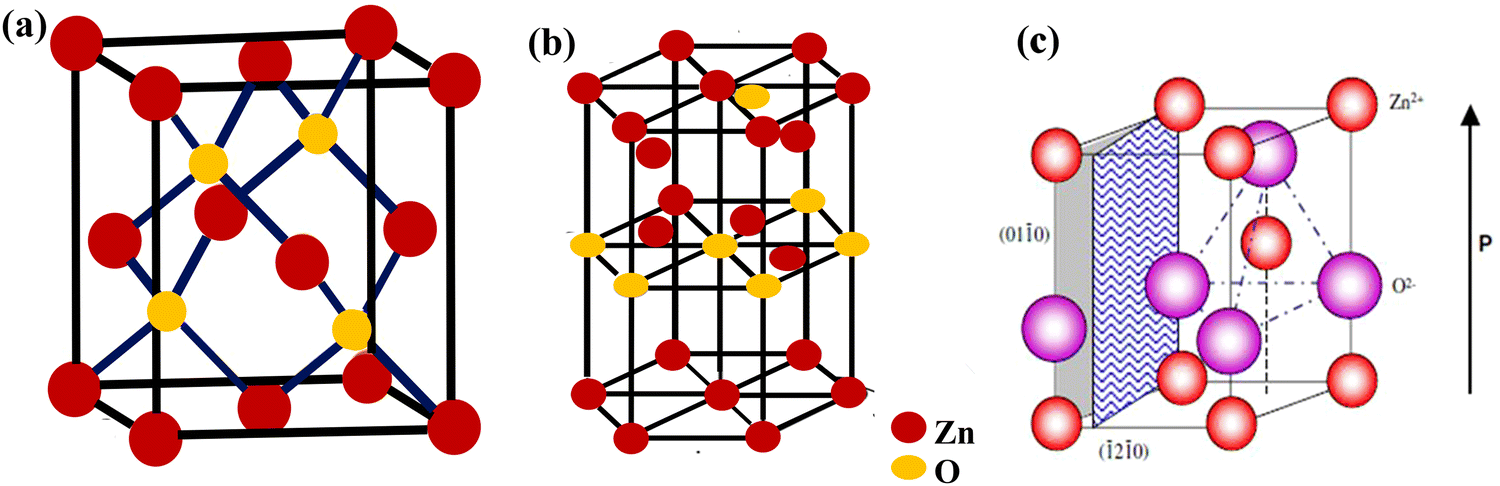 | ||
| Fig. 2 (a) The zinc blende crystal structure of ZnO. (b) The wurtzite crystal structure of ZnO. (c) The wurtzite structure model of ZnO showing the tetrahedral arrangement of Zn and O in the ZnO crystal structures. Reprinted with permission from ref. 89. Copyright 2004 IOP Science. | ||
ZnO has characteristics polar surfaces with a basal plane as a common polar surface. The positively charged Zn-(0001) and negatively charged O-(000![[1 with combining macron]](https://www.rsc.org/images/entities/char_0031_0304.gif) ) surfaces form spontaneous polarization along the c-axis, and creates a normal dipole moment. To maintain a stable structure, the polar surfaces usually exhibit massive surface reconstructions. However, ZnO-±(0001) are atomically flat, stable, and form without reconstruction.93,94 These unique structural properties make ZnO as a functional nanomaterial for advanced applications. The nanorods, nanowires, nanoring, nanospring, nanocomb, nanocages, nanotetrapods and many more morphologies of ZnO bring extraordinary changes in the material properties.89,95,96
) surfaces form spontaneous polarization along the c-axis, and creates a normal dipole moment. To maintain a stable structure, the polar surfaces usually exhibit massive surface reconstructions. However, ZnO-±(0001) are atomically flat, stable, and form without reconstruction.93,94 These unique structural properties make ZnO as a functional nanomaterial for advanced applications. The nanorods, nanowires, nanoring, nanospring, nanocomb, nanocages, nanotetrapods and many more morphologies of ZnO bring extraordinary changes in the material properties.89,95,96
Among various morphologies, the tetrapod shape-like nanostructure has several advantages over the other morphologies of ZnO or its bulk counterpart because of its spatial distribution between the arms. One of the key advantages of the tetrapod morphology is its automatic orientation on the substrate with one of its arms directed to the surface of the substrate. The tetrapod is the simplest structure consisting of rod-shaped structures joined at a tetrahedral angle to the central core.53,97–100 Various researchers have reported the growth of the ZnO tetrapod via various routes. The nucleation and growth kinetics of the ZnO enable it to crystallize in both hexagonal wurtzite and cubic blende structure, allowing the formation of the tetrapod-like morphology, where the four-wurtzite hexagonal arm extends to the surrounding space to form a central zinc blende core structure.101,102 The wurtzite and zinc blende structure of ZnO forms the shared intermediate facets between the two crystal structures. This leads to the formation of the tetrapod geometry.103 During the nucleation and growth process, the stability of these two crystal structures is important for the formation of the tetrapod structure. During the nucleation process, the zinc blende structure formation takes places. However, it is dominated by the wurtzite structure. This tetrapod structural design has the capability to form a good network with tailored mechanical strength. The tetrapod structural morphology of the ZnO nanostructures is displayed in Fig. 3.
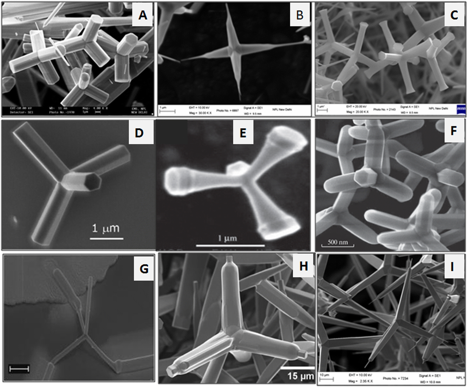 | ||
| Fig. 3 Tetrapod morphologies of the ZnO nanostructures (a–c) prepared by thermal evaporation method. (d) SEM image of a single tetrapod. Reprinted with permission from ref. 96. Copyright 2007 Elsevier. (e) Trumpet-shaped ZnO tetrapod. Reprinted with permission from ref. 104. Copyright 2003 John Wiley and Sons. (f) Tetrapod morphology. Reprinted with permission from ref. 105. Copyright 2019 Springer Nature. (g) Tetrapod with electrodes for IV measurements. Reprinted with permission from ref. 106. Copyright 2006 AIP Publishing. (h) Tetrapod structure. Reprinted with permission from ref. 107. Copyright 2015 American Chemical Society. (i) Tetrapod structure with a fine tip at the end. | ||
If all of the arms of the tetrapods are uniform and less than 100 nm, then these are termed as ZnO nanocrystals (0-D).1 Moreover, if the length of one of the arms of the tetrapod is less than 100 nanometers, then it is known as a 1-D nanostructure. Finally, if the lengths of the arms are random in size (from nanometer to micrometer), then it is known as a 3-D nanomaterial. However, in the literature, the tetrapod geometries of the ZnO nanostructures are mostly known as 3-D nanostructures. Several synthesis processes have been developed to obtain the ZnO tetrapod structures, including the thermal evaporation process, atmosphere-controlled oxidation, microwave radiation, catalytic oxidation and self-combustion methods.104,108–111 To obtain the ZnO tetrapod structures, the synthesis technique is composed of two categories. The first approach is started with the solid phase leading to a solid vapor transport condensation method, and the second one is the liquid reaction process. However, there are other several crucial aspects in terms of size, quantity, quality, yield and stability of the ZnO tetrapod structures, which depend on various parameters during the synthesis process, such as the temperature, heating rate, and the evaporation pressure of the Zn and O molecules during nucleation and growth kinetics. The continuous synthesis of the ZnO tetrapod at a large scale (in grams) by employing the combustion of micron-sized Zn particles was developed by S. Rackauskas et al. in 2015.112 Furthermore, the ZnO tetrapod nanostructures were studied for structural modification112,113 with optical and transport properties114 for future nanomaterial-based devices.
J. S. Tawale et al. have proposed the growth mechanism of the ZnO tetrapod on the basis of the nucleation, crystal structure and surface energy.113 The formation of the ZnO nanorod is shown in Fig. 4. Nucleation is a critical step for obtaining the required shape of the ZnO nanostructures. The crystallographic growth of the resulting structures is also governed by the formation/addition of reactive particles, which act as nucleation sites for metal reduction. This also changed the kinetics of the nanocrystal growth process. It was believed that the zinc blende phase plays a significant role in getting the tetrapod structures, which were also confirmed by HR-TEM studies.115 It was proposed that the center of the ZnO tetrapod possesses a ZB structure, which nucleates into four arms via the preferred growth planes of (0002) and (1000), as shown in Fig. 4a. The strongest ionic bonding of ZnO among the group leads to the formation of the highly stable wurtzite phase, which was confirmed by XRD results. Furthermore, the growth of the flower shape morphology from the tetrapod morphology in silver (Ag)-doped ZnO is shown in Fig. 4b. The tetrapod to flower shape transformation in morphology is achieved via silver (Ag) doping in ZnO. As shown in Fig. 4, at the atomic level, a higher number of nucleation facets are grown. This resulted in the fast growth of other planes of the hexagonally closely packed (hcp) structure taking place, and the flower-like morphologies were formed. The doping of the Ag+ ions in ZnO may also be an additional nucleating agent without symmetry breaking of the hexagonal unit cell. The anisotropic growth of the flower shape ZnO structure is formed by interaction with various crystal faces.
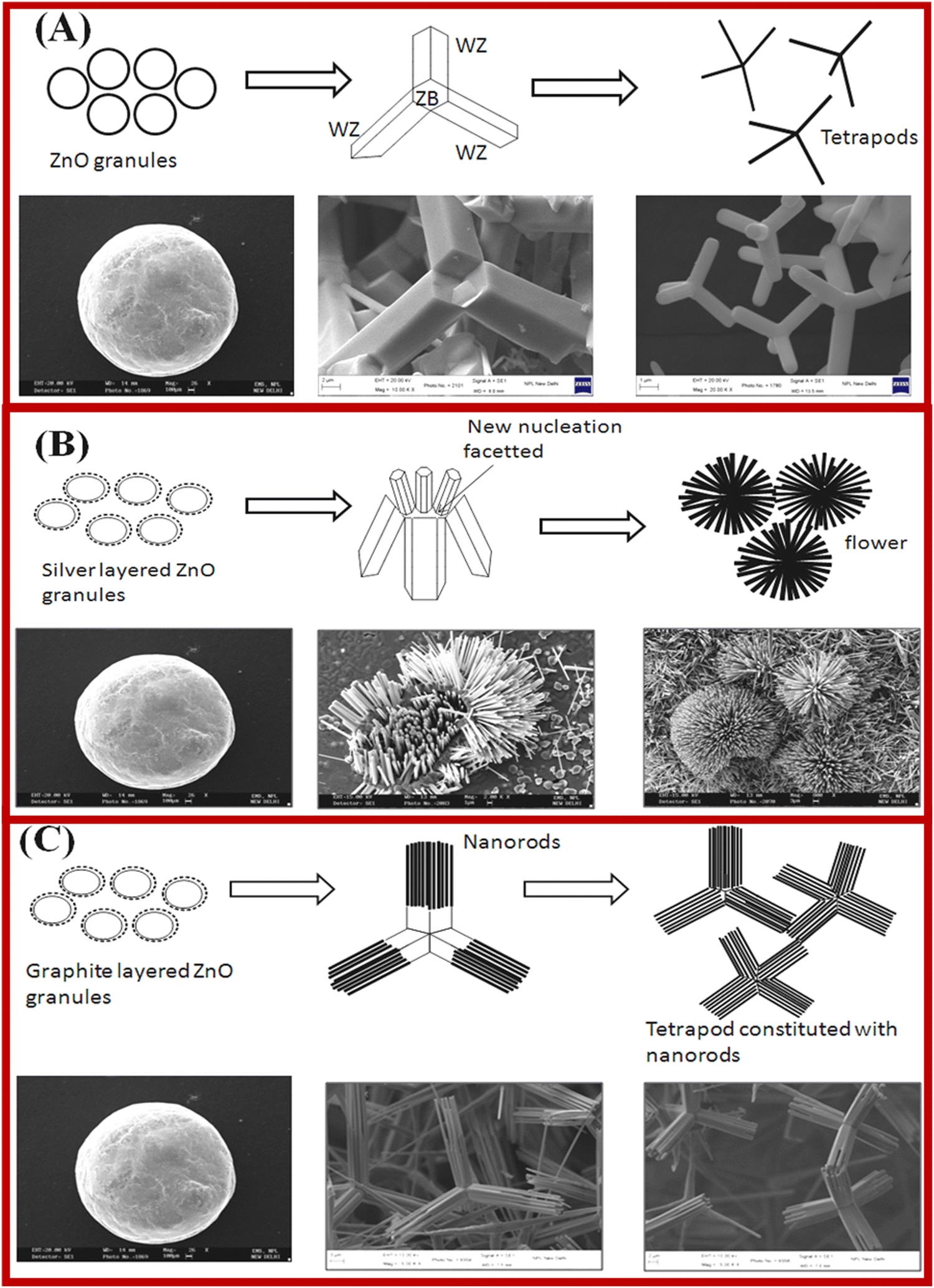 | ||
| Fig. 4 Presentation of ZnO tetrapod structures nucleation and growth kinetics, and microstructural transformation with Ag and graphite doping. (a–c) ZnO, Ag-doped ZnO and Gr-doped ZnO. Reprinted with permission from ref. 116. Copyright 2013 Elsevier. | ||
The effect of the graphite on the structural transition in ZnO nanostructures is shown in Fig. 4c. The TEM results reveal that the tetrapod morphology of ZnO constitutes nanorods that are nucleated from the tetrapod center. The ZnO nanocrystals exhibit twin planes. The anisotropic growth and twin planes under high temperature result in the formation of a tetrahedral geometry of ZnO in the presence of highly anisotropic graphite. The controlled growth of the ZnO nanostructures with the addition of graphite and silver showed a path to overcome the challenges in the fabrication of efficient devices.116
As compared to other morphologies of ZnO, the multidimensional growth of the ZnO tetrapod makes this a fascinating material for multifunctional applications.117 In nanoscale ZnO tetrapods, the electron conduction properties is better as compared to other morphologies for application in photovoltaic devices.118 Various ZnO tetrapod nanostructures were also fabricated via different synthesis approaches, and are widely studied for sensor applications108,119–122 and hybrid logic switches applications.123 Moreover, the tetrapod nanocrystals have been successfully used in solar cells,110,124,125 lasers,126 and field emission127 applications due to their fascinating semiconductor and absorption properties.128 Furthermore, various efforts have been focused on tuning the electrical, optical and sensing characteristics of the ZnO tetrapod by doping. Doped ZnO tetrapods-based nano devices have also been fabricated by various researchers.107 Similarly, ZnO tetrapod materials have successfully been used as reinforced materials for composites nanostructures. The branched nanostructure of the ZnO tetrapods is used as a reinforced material with graphene, polymers and other matrices to enhance the optical and electron transport properties for higher efficiency.
In particular, the morphology of the semiconducting piezoelectric 2D ZnO nanostructures has significantly tuned the output performance of the nanogenerators, and also altered the charge generation polarity such as from AC to DC type signals under vertical compression. 2D ZnO nanosheets have been utilized as well for 2D piezotronics device application.129,130
2.2 SnO2 nanostructures and its morphological properties
Tin dioxide is an inorganic semiconductor material with the chemical formula of SnO2. SnO2 is also known as cassiterite and has a rutile crystal structure.131,132 The unit cell of SnO2 exhibits tetragonal rutile, cubic pyrite and cubic fluorite crystal structures and SnO2 exhibits the most stable phase of the tetragonal rutile structure (Fig. 5).132 The rutile SnO2 has a tetragonal unit cell with a lattice constant of a = 0.473, b = 0.473 and c = 0.318 nm with the P42/mnm space group. The structural geometry of the SnO2 crystal is described as tin (Sn) atoms are six-fold and the oxygen (O) atoms are threefold coordinated. In addition, SnO2 has high electron mobility, conductivity and high optical transparency.131 Due to its large bandgap, high stability under heat, light and moisture conditions, and easy fabrication process, SnO2 has been widely used in perovskite solar cells (PSCs) and dye-sensitized solar cells (DSSCs), lithium-ion batteries, supercapacitors, gas sensors and catalysis applications.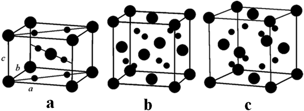 | ||
| Fig. 5 Crystal structures of the SnO2 nanostructures: (a) tetragonal rutile, (b) cubic pyrite, (c) cubic fluorite. Large and small circles represent the Sn and O atoms, respectively. Reprinted with permission from ref. 132. Copyright 2012 Springer Nature. | ||
SnO2 is an n-type semiconducting oxide nanostructure with a wide band gap of 3.6 eV at 300 K and large exciton binding energy of 130 eV. The SnO2 possesses unique electrical and optical properties like low resistivity (10−4 to 106) Ω cm−1, high optical transparency and excellent chemical stability. These excellent properties make the SnO2 nanomaterial useful for various applications, such as ceramic glazing, polishing, glass coating and in gas sensing. The bandgap of SnO2 has been reported to be in the range of 3.5 eV to 4.0 eV. Depending on the synthesis conditions, the band gap also changes. It has a high transmittance value of 90% in glass due to the high bandgap and small refractive index. SnO2 also has a high electron mobility of 240 cm2 V−1 s−1, which is about 100 times higher than that for TiO2. At the nanoscale, SnO2 materials with different shapes and sizes exhibit different optical and electrical properties compared to the bulk form. The SnO2 nanostructure has remarkable receptivity variation in gaseous environments, and it has been used for sensing and solar applications. The SnO2 nanostructure is mostly studied for catalyst,133 varistor,134 field emission,135 UV sensors,136 sensors,137–139 solar cells,140,141 and lithium-ion battery applications.142,143 The intriguing morphology of the SnO2 nanostructures, such as nanoparticles, nanowires, nanorods, nanotubes, nanosheets, nanobox and hierarchal structures, has been successfully synthesized and reported for various applications.144–150
The fascinating morphology of the SnO2 nanostructures, such as spherical, nanoribbons, nanotubes, nanobox, nanowires, square-shaped nanotubes, and octahedral (which are prepared by several novel synthesis routes), is shown in Fig. 6. The fundamental understanding about the nucleation and growth kinetics of these nanostructures (dimensional morphology) played an important role to achieve these various properties and tune their application. Furthermore, surface modifications, doping and synthesis/reaction parameters and nanostructures are major routes to change the morphology of SnO2. There are different mechanisms discussed in the literature for the nucleation and growth kinetics of SnO2 nanostructures. In particular, the electron microscopy technique is one of the ways to explore the growth mechanism and nucleation kinetics of nanostructures. The schematic image of the growth kinetics mechanism of the SnO2 octahedral nanostructures is illustrated in Fig. 7.
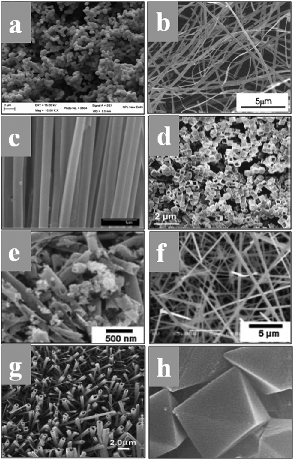 | ||
| Fig. 6 (a) Faceted spherical nanostructures of SnO2. (b) Large scale SnO2 nanoribbons by the rapid oxidation synthesis method. Reprinted with permission from ref. 145. Copyright 2002 American Chemical Society. (c) Polycrystalline SnO2 nanotubes prepared by infiltration casting of nanocrystallites. Reprinted with permission from ref. 146. Copyright 2005 American Chemical Society. (d) Fast formation of SnO2 nanoboxes for energy applications. Reprinted with permission from ref. 147. Copyright 2011 American Chemical Society. (e and f) Nanotubes and nanowires of SnO2. Reprinted with permission from ref. 148. Copyright 2008 John Wiley and Sons. (g) Array of square-shaped SnO2 nanotubes. Reprinted with permission from ref. 149. Copyright 2005 John Wiley and Sons. (h) Self-constructed SnO2 octahedral nanostructures based on the aggregation of nanocrystallites. Reprinted with permission from ref. 151. Copyright 2004 John Wiley and Sons. | ||
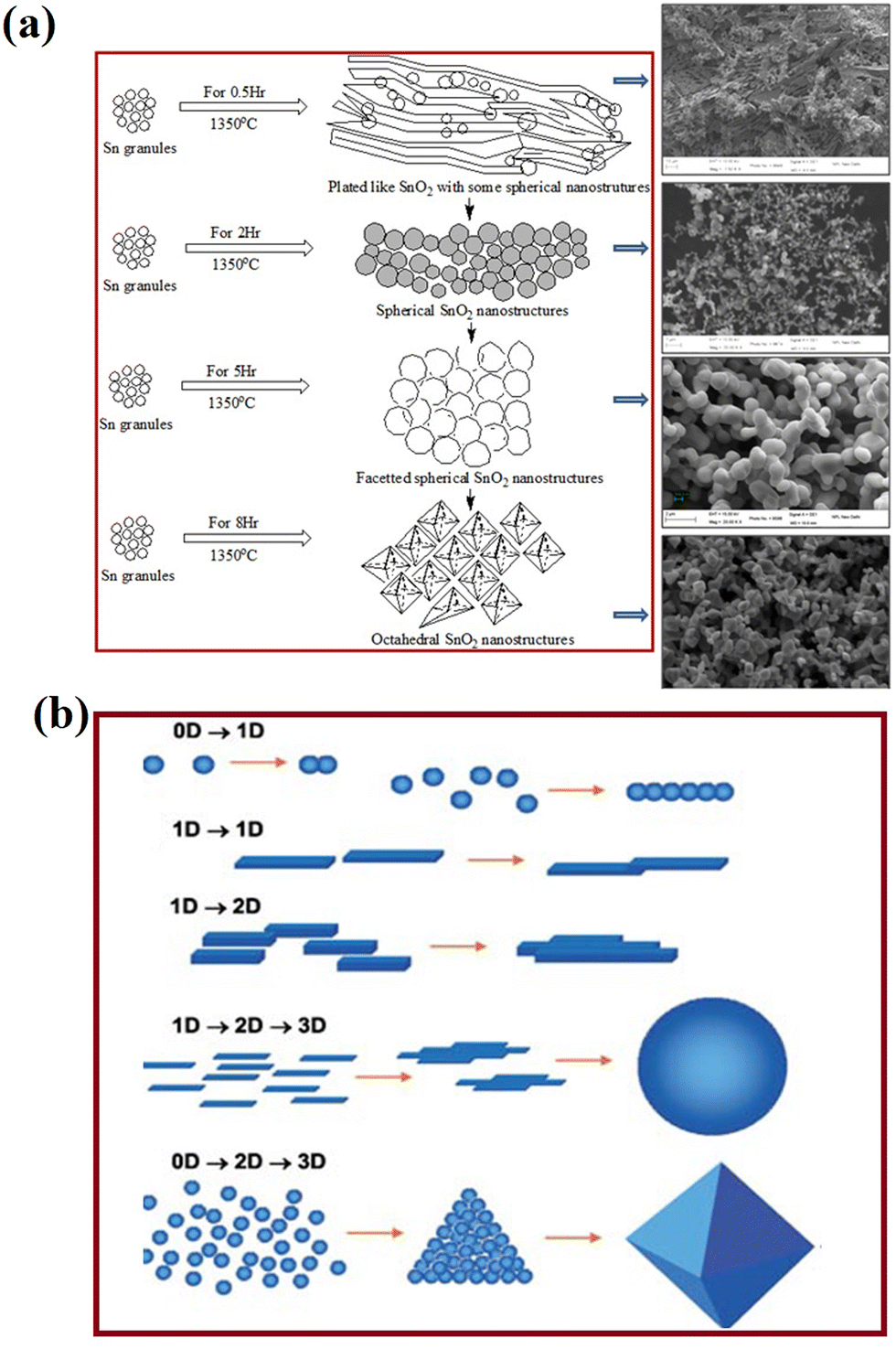 | ||
| Fig. 7 (a) Schematic of the SnO2 structural growth phenomena and morphological transformation with increasing evaporation time during thermal evaporation at 1350 °C. Reprinted with permission from ref. 152. Copyright 2014 Elsevier. (b) Various organizing schemes for the self-construction of nanostructures by oriented attachment. Reprinted with permission from ref. 151. Copyright 2004 John Wiley and Sons. | ||
The schematic image reveals the self-oriented growth mechanism of nanostructures on the basis of dimensional confinement (Fig. 7). The 1-D nanostructures (e.g., nanorods, nanotubes) are obtained from the symmetrical accumulation of the 0-D nanostructures. Further self-orientation of these 1-D nanostructures results in 1-D or 2-D structures, depending on the interactions among the surfaces of the nanostructures during the synthesis process. In the layered structures, the stacking of layers is caused by the planar van der Waals attraction and in ionic compounds. Furthermore, these self-oriented growths of nanostructures also lead to the formation of 3-D nanostructures like spherical, tetrapod or octahedral structures. It was reported that the structural modifications in SnO2 nanostructures have a strong influence on optical properties like absorption and defect emissions.153–155 Various experiments have been reported, including metal ion doping in SnO2 nanocrystals for improvement in the structural and optical properties for technological purpose.156–158
The sensing properties of metal oxide nanomaterials have considerable research interest because of their high surface-to-volume ratio and suitable surface chemistry for a variety of sensor applications. A sensor is basically a device that measures the physical quantity of an analyte of interest and converts it into a readable signal. For example, a humidity sensor senses, measures, and reports the relative humidity in air, and gas sensors are known for the detection of inflammable or toxic gases.30,159,160 Owing to their low cost and flexibility in fabrication, simplicity of use, large number of detectable gases and possible application, the semiconducting oxide nanomaterials are one of the most investigated groups for sensing properties. Oxide nanostructures with modified structural, optical and electrical properties have opened up the potential application in sensor devices with high sensing, low detection limits, low power consumption and high compatibility. The sensing properties are mostly influenced by the microstructure, surface modification by metal particles, and chemical composition of the materials. The environment conditions (temperature and relative humidity) are essential factors and matters of great concern for high-end sophisticated measuring and processing instruments in the storage and food sectors. The development and fabrication of humidity sensor devices based on new nanostructured materials are a continuously growing field for various applications. The sensing measurement results demonstrated that the water vapor in the air has a strong influence on the conductivity of the metal oxide nanostructure, and SnO2 is one of the most suitable candidates for humidity sensing application. The SnO2 nanostructures have also been widely used in humidity sensors. Due to the large band gap and low efficiency in the excitation and recombination process, SnO2 has been used in numerous applications.161–164 This extraordinary electron transition results in better sensing performance. The large surface-to-volume ratio and channel or network of the SnO2 nanostructures offer enhanced sensitivity. Moreover, SnO2 is an excellent material for the fabrication of solid-state gas sensors, and the long-term structural stability of SnO2 nanostructures has been largely investigated for temperature-dependent metal oxide gas sensor operation.164 Ultra-thin layers of SnO2 and its integration with CMOS has been extensively applied for sensitive gas detection. SnO2 nanostructures in the form of ultra-thin layers are used for the development of smart sensor devices, like CMOS integration of gas sensitive materials in daily life applications. The various aspects of thin layers of SnO2 on CMOS chips have been studied for the technological importance of the devices and sensing performance.162–164 The operating characteristics of the sensors are determined by both receptor and transducer functions, and consequently determines the efficiency of the chemical interaction and conversion into electric signals. Therefore, the morphology and crystallographic structure of the SnO2 nanostructure are crucial properties for improving the performance of sensors. The recovery time, sensitivity, and reproducibility of the response of the sensors can be significantly increased or modified by the grain size, crystallinity, and morphology of the materials. The surface modification strategies, including doping states on the surfaces of the metal oxides, can be achieved by novel sol–gel, thermal evaporation and other synthesis methods. Moreover, the adsorption ability, sensitivity and catalytic activity also affect the sensor performance.165–168
3. Solar cell applications of metal oxide nanostructures
3.1 ZnO nanostructures-based solar cell
Sensitized solar cells (SSCs) provide a cheap, flexible and durable alternative to conventional silicon-based solar cells with reasonably high power conversion efficiencies.169 ZnO nanostructures have been used as the photoanode. Various techniques have been used to increase the power conversion efficiency (PCE) of SSCs, such as optimizing the size of the nanorods and the crystallographic orientation.170 Due to the n-type semiconductor property, high electron mobility, excellent photoluminescence, high conductivity, ease of fabrication and high thermal stability, ZnO has been extensively used in solar energy harvesting, especially in sensitized solar cells and heterojunction solar cells. Surface modifications in the ZnO nanostructure have been reported to tune the absorption spectra, and provide a high diffusion coefficient and electron mobility via the use of gold nanoparticles and doping with aluminium.171,172 ZnO nanotubes have also been used as photoanodes, which showed increased PCE because of the higher surface area.173,174 Since ZnO is not compatible with the most commonly used Ru-based dyes,175 metal-free dyes176–178 have been used to increase the PCE of ZnO-based solar cells to >5%. Doping of ZnO thin films with various elements such as iodine has been also utilized to further increase the PCE of solar cells to beyond 20%.179 Furthermore, ZnO nanostructures have been used in perovskite-sensitized solar cells as an electron transport layers (ETL) for interfacial engineering to enhance the device performance (Fig. 8). Incorporation of cone-like ZnO with the c-TiO2 as a part of ETL improves the charge transfer at the ETL-perovskite interface, and also leads to a reduction in the recombination losses. This led to better J–V characteristics (Fig. 8(a)) and higher PCE for c-TiO2 and the cone-shaped ZnO bilayer ETL (Fig. 8(b–d)). This bilayer also had the lowest reduction in PCE (device degradation) as a function of time, highlighting the importance of ZnO in improving the device stability by suppressing the chemical reactions at the ETL-perovskite interface.180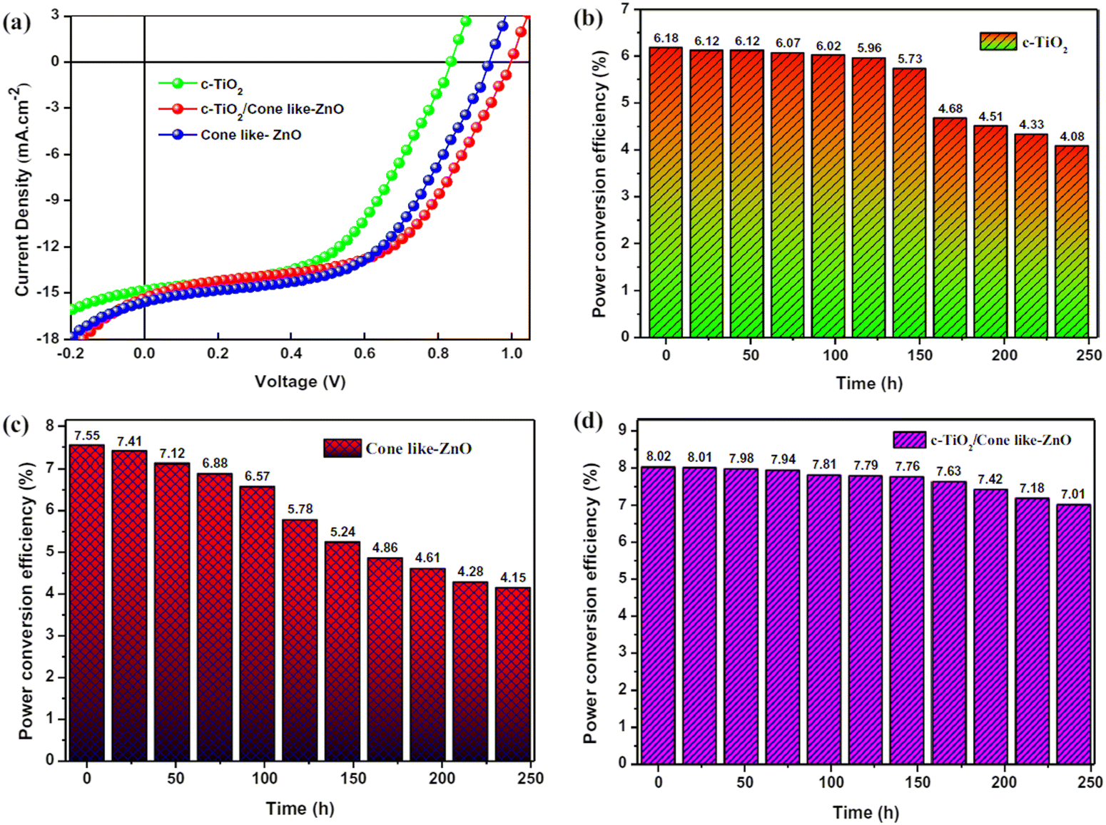 | ||
| Fig. 8 Use of cone-like ZnO improves the perovskite solar cell performance. (a) Better J–V characteristics of upon addition of the cone-like ZnO as a part of ETL. (b–d) PCE over time for the single layer c-TiO2, cone-like ZnO and bilayer of c-TiO2 with come like ZnO as ETL. Reprinted with permission from ref. 180. Copyright 2021 Springer Nature. | ||
It has been reported that the morphology of ZnO also plays a significant role in improving the PCE efficiency, and ZnO nanoparticles exhibit better efficiencies than nanorods as the 1D structures provide direct electron pathways for electron transport.181 The electrons suffer several trapping and detrapping events, especially at the grain boundaries of nanoparticles.182,183 Doping in ZnO can also increase the PCE of solar cells by multiple ways, such as by increasing the carrier concentration, carrier mobility and conductivity, while reducing the internal resistance, and promoting electron extraction from the perovskite layer.184,185Fig. 9 summarizes the key application areas of nanostructured ZnO in solar cells.186
 | ||
| Fig. 9 Application of the ZnO-nanostructured solar cell. Reprinted with permission from ref. 186. Copyright 2020 Royal Society of Chemistry. | ||
It was observed that depending on the doping elements, the morphologies of the ZnO nanostructure changed. This resulted in the interface interaction between the perovskite and ZnO nanostructure increasing, causing the work function to decrease, which facilitated the easier extraction of an electron into the ZnO layer.187,188 Using the doping methodology in ZnO, solar cells with PCE >21% have been fabricated.189 The PCE of these SSCs depends on the number of free electrons, back transfer of electrons from ZnO, and the total surface area of ZnO. In heterojunction solar cells, ZnO is used as an n-type semiconductor in the active layer,190,191 an electron transport,192,193 or a buffer layer.194 However, the solar cells required more optimization to improve the power conversion efficiencies compared to conventional solar cells. In the organic solar cells, ZnO has also been used as a cathode buffer layer where power conversion efficiencies as high as 15.7% have been observed.195 ZnO nanostructures have also been used as a part of the anti-reflection layer in CSZTe and Si solar cells, leading to a reduction in the reflection from 7.76% to 2.97%.196,197 Further enhancements in the performance of the ZnO nanostructures-based solar cells can be made by increasing the surface area, which can allow for increased rate of kinetics during solar cell functioning, and by enhancing the light absorption capability.
3.2 SnO2 nanostructures-based solar cell
Due to the large bandgap, good transparency in the optical spectrum, low refractive index, and high stability, SnO2 nanostructures have been extensively used for solar energy-harvesting applications.198 Various nanostructures of SnO2 have also been used to fabricate the solar cell. In particular, SnO2 nanowires with few defects such as grain boundaries have been used to fabricate the dye-SSCs, as well as perovskite solar cell PSCs.199–201 Very high PCEs of 14.2% were obtained from the SnO2-based nanowires-based solar cells.202 Nanorods have an open porous structure, which allows for more efficient filling by the perovskite crystals, leading to enhanced light absorption203,204 and PCE of 18.7% from the solar cells.205 SnO2 nanotubes with high electrical conductivity are also used to fabricate the solar cell, and an efficiency of about 12.1% has been achieved.206 The SnO2 nanosheets used to promote the interfacial charge transfer was used to fabricate the solar cell. The nanosheets showed high photo-induced carrier collection,207,208 and a very high PCE of 18.3% was reported.209 The performance of the solar cell was also achieved by passivation of the SnO2–pervoskite interface to suppress defects, such as Sn interstitials, O vacancies, and film cracking, which would degrade the device performance.210,211 Various strategies, such as doping with metals and halogens (which also improves the energy level alignment212–214), bilayer ETLs using various oxides,215–217 interface modification with ammonium salts,218,219 and quantum dots220 have been employed to suppress these defects and increase the PCE of the solar cell. The highest PCE using SnO2 in a perovskite solar cell has been reported to be 25.2%. The SnO2-based perovskite solar cell showed longer durability compared to the TiO2-based perovskite solar cell.221–223Fig. 10 (inset) shows a schematic of a perovskite solar cell fabricated with a hybrid ETL of mesoporous TiO2/amorphous SnO2 (mp-TiO2/a-SnO2). As can be seen in Fig. 10, the a-SnO2 addition leads to reduced hysteresis in the J–V curve because of a better bandgap alignment, which leads to the fast electron extraction from the perovskite. This also leads to a reduction in the nonradiative carrier recombination, which improves the VOC by ∼170 mV and PCE of mp-TiO2/a-SnO2 by ∼1.5%. It has also been reported that the addition of a mp-SnO2 layer instead of a planar SnO2 ETL layer acts as an energy bridge by facilitating energy transfer from perovskite to SnO2, and also increases the contact area for more efficient extraction. This leads to lower hysteresis losses and higher PCE with mp-SnO2, as compared to that with planar SnO2, as can be seen in Fig. 11a. Moreover, mp-SnO2 inhibits degradation of perovskite and prevents the penetration of harmful substances, such as moisture, oxide or gold into the perovskite layer, leading to much better stability and lower degradation of PCE over time (Fig. 11b).224 Because of its low temperature processability and stability, SnO2 has sparked a lot of interest as ETL for flexible perovskite solar cells.224–226 However, controlling the processing temperature and crystallinity defects is required to fabricate high-performance SnO2-based flexible devices.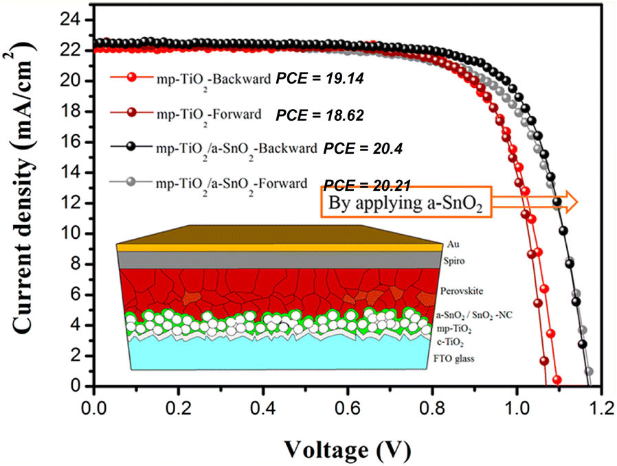 | ||
| Fig. 10 Cross-sectional SEM image of the perovskite solar cell based on mp-TiO2/a-SnO2. J–V curves for mp-TiO2 and mp-TiO2/a-SnO2 along with the power conversion efficiencies. Inset shows a schematic of a perovskite solar cell based on mp-TiO2/a-SnO2. Reprinted with permission from ref. 227. Copyright 2018 American Chemical Society. | ||
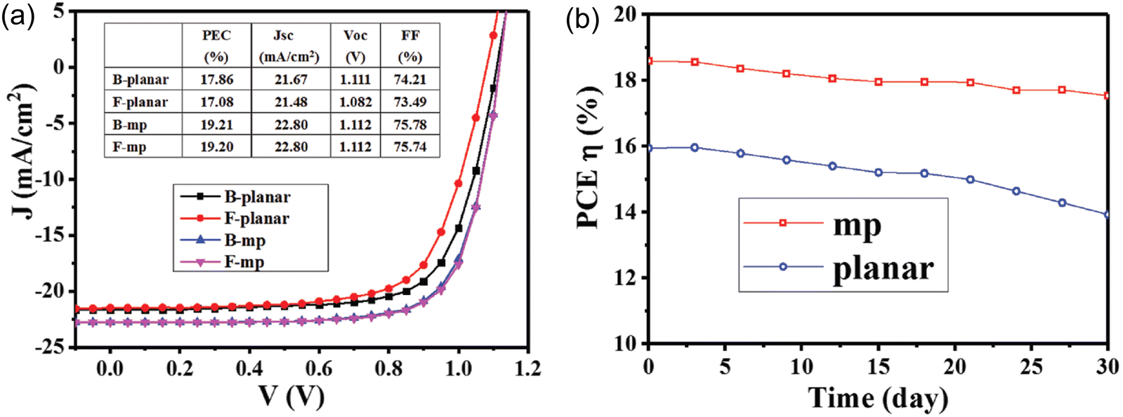 | ||
| Fig. 11 (a) J–V graphs obtained of the planar SnO2 and mp SnO2 PSCs from under backward and forward voltage scanning. (b) PCEs of the planar SnO2 and mp SnO2 PSCs monitored every 3 d; the measurement was performed under AM 1.5G with input solar power Pin of 100 mW cm−2. Reprinted with permission from ref. 224. Copyright 2018 John Wiley and Sons. | ||
4. Biological applications
4.1 Antimicrobial application of ZnO nanostructures
ZnO nanoparticles (NPs) possess unique physicochemical and structural properties, including shape, particle size, zeta potential, crystallinity and porosity, which make them attractive as antimicrobial agents. ZnO NPs show effectiveness against different types of microbes, fungi, viruses, and Gram-positive and Gram-negative bacteria.228 In one study, Faisal et al.229 synthesized ZnO NPs from the fruit extract of Myristica fragrans, which function as a reducing, capping and stabilizing agent for NPs. Their antibacterial activity against bacterial species, such as E. coli, P. aeruginosa, K. pneumoniae and S. aureus, was analyzed.229 The obtained results indicate that the maximum zone of inhibition (ZOI) was displayed when these NPs were treated with K. pneumoniae, with 27 ± 1.73 mm as compared to 15 ± 1.54 mm, 17 ± 1.66 mm and 21 ± 1.73 mm for E. coli, P. aeruginosa and S. aureus, respectively. The authors suggested that bioactive compounds present in the plant-mediated synthesis process possess therapeutic activities.228aThe widely accepted plausible mechanism is that the generation of the reactive oxygen species (ROS) is responsible for the antibacterial action of ZnO NPs. ROS can break the chemical bonds of the organic matter present in bacteria, and cause a bactericidal effect (Fig. 12).228b Moreover, nano-sized particles release metal ions that can lead to cell content leakage, lipid peroxidation, oxidative stress, cytoplasm leakage, protein denaturation and DNA damage.230–232 It has also been reported that ZnO NPs show efficacy against bacterial species in the dark, and it is more significant at low bacterial concentration. In a dark environment, some additional mechanisms might take part, such as the release of Zn2+ ions penetrating the bacterial moiety, causing protein denaturation and cellular respiratory disorder (Fig. 12b).
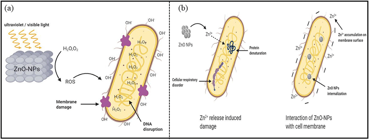 | ||
| Fig. 12 Antibacterial mechanism of ZnO NPs through (a) ROS production, causing a bactericidal effect, (b) Zn2+ ions release in a dark environment. Reprinted with permission from ref. 228b. Copyright 2020 Frontiers. | ||
When communities of bacteria adhere to the surface and are embedded in extracellular polymeric substances (EPS), they form a biofilm. The bacterial biofilm is highly resistant to any antibiotics or traditional biocidal drugs. Different types of biofilms are formed in wound beds, and therefore complicate the wound healing process. ZnO NPs have shown improved antimicrobial properties against planktonic bacteria and bacterial biofilms. Rayyif et al.233 found ZnO NPs-coated polyester-nylon wound dressings to be effective against planktonic (Gram-positive and Gram-negative) and biofilm-embedded bacterial strains. Bacterial viability was analyzed in a time- and dose-dependent manner. For Gram-positive bacteria (S. aureus and E. faecalis), substantial viability loss was observed at least at 12 h of incubation, which was higher than that of the case of Gram-negative bacteria. Viability loss was 6 h of incubation for the strains of P. aeruginosa and E. coli. The difference in their viability loss was related to their cell wall composition, as Gram-positive bacteria possess a thick peptidoglycan cell wall. Thus, the Gram-negative bacterial cell wall was more susceptible to be pierced by ZnO NPs. Biofilm inhibition was observed at 48 h for S. aureus, E. faecalis, and E. coli at 0.6 and 0.9% ZnO-coated dressings, while the P. aeruginosa biofilm was observed to be reduced after 72 h of incubation. Thus, ZnO-based dressings could be effectively used to deal with chronic wounds.
Moreover, ZnO nanostructures were observed to be effective against many viruses, such as herpes simplex virus type 1 (HSV-1),234,235 Hepatitis A virus (HAV),236 human metapneumovirus,235 and a virus from the Coronaviridae family. Billions of people worldwide were infected through a severe acute respiratory syndrome coronavirus 2 (SARS-CoV-2). The WHO declared the virus outbreak as a Public Health Emergency of International Concern as it is a pandemic threat. SARS-CoV-2 has morphological similarity with NPs, as it is an enveloped virus with particle-like features and possesses a radius in the range of 30–70 nm.237 Thus, NPs have immense potential to mimic and tackle this virus.
Firstly, it is necessary to gather information about the structural proteins present in the SARS-CoV-2 protein. SARS-CoV-2 is a single-stranded and enveloped ribonucleic acid virus. As shown in Fig. 13a, the spike surface glycoprotein (S), matrix protein (M), small envelope protein (E), and nucleocapsid protein (N) are the four structural proteins of SARS-CoV-2. The U.S. National Institute of Allergy and Infectious Diseases (NIAID) has released electron micrographs revealing the morphology of SARS-CoV-2, as shown in Fig. 13(b–e).238
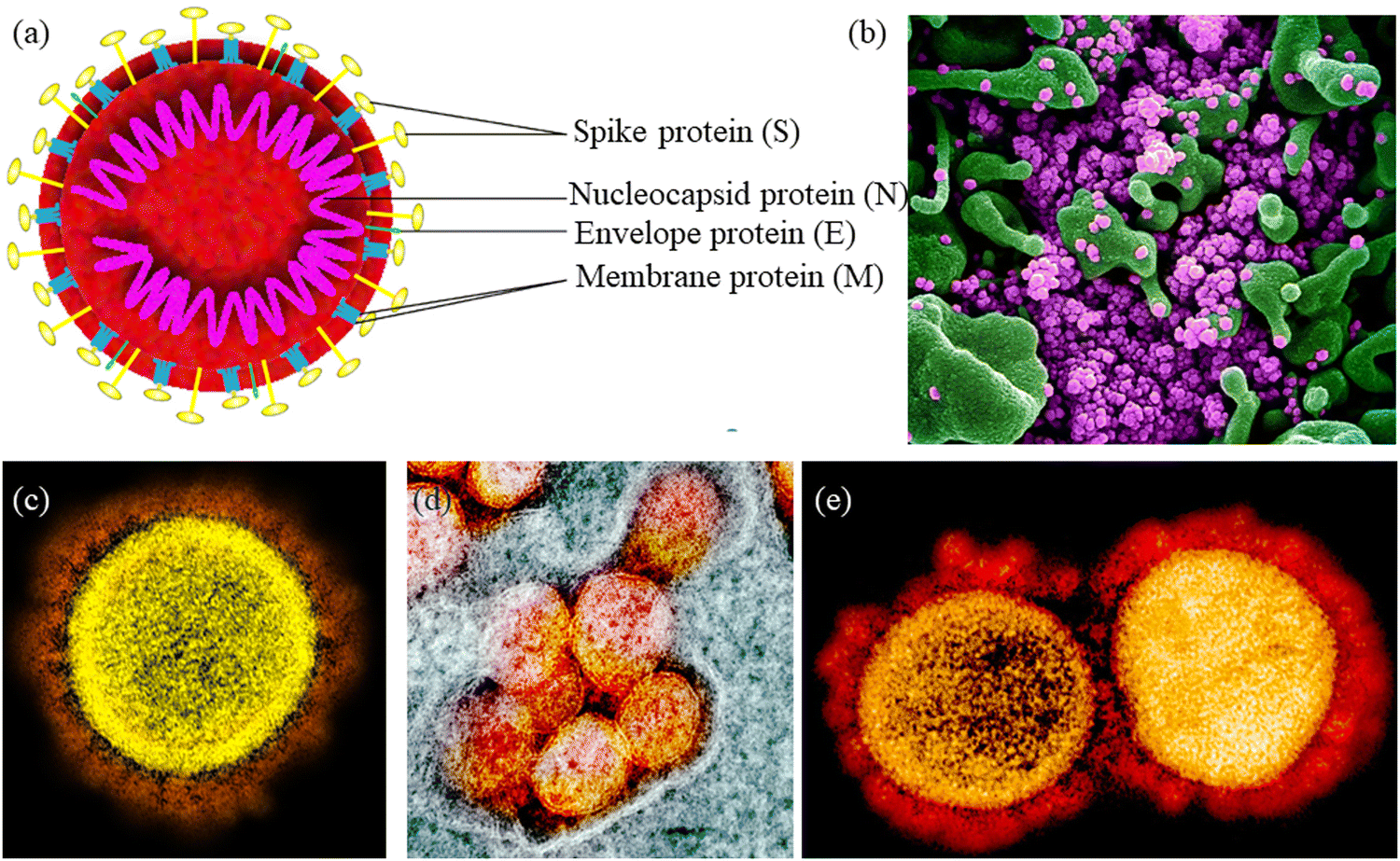 | ||
| Fig. 13 (a) Structure of SARS-CoV-2. Reprinted with permission from ref. 238. Copyright 2020 Elsevier. (b) Scanning electron microscopy (SEM) image showing SARS-COV-2 virus particles (purple) in apoptotic cell (green). (c–e) Transmission electron micrograph (TEM) of SARS-CoV-2 virus particles, isolated from a patient. (b–e) Photo Credit: NIALID. | ||
Tavakoli et al.235 demonstrated the antiviral activity of ZnO NPs and PEGylated ZnO NPs (polyethylene glycol-coated ZnO NPs) against HSV-1. The authors reported that after coating the NPs with PEG, the antiviral activity was improved compared to only ZnO NPs at the same concentration. That may be due to less agglomeration by surface coating these NPs with PEG, and it could be considered as an effective agent for enhancing antiviral activities. Generally, the reason why ZnO NPs possess potency against many viruses could be that Zn has antiviral activity, and thus it can (i) prevent the entry of the virus, (ii) prevent the replication of the virus, and (iii) trigger ROS, which lead to oxidative injury and cell death.
Similarly, Attia et al.236 investigated the antiviral activity of ZnO NPs of 20–30 nm size (estimated by TEM) against HAV with 58.83% at the maximum non-cytotoxic concentration. However, the authors have not mentioned the plausible mechanism behind it.
4.2 Antilarvicidal activity of ZnO nanostructures
Mosquitoes, such as Aedes aegypti and Aedes albopictus, are the primary vector to transmit the deadly disease, dengue. Not only dengue, but yellow fever, Chikungunya, and Zika virus are also transmitted by these mosquitoes. Malaria is the prevalent mosquito-borne disease that is caused by Anopheles. To combat these deadly diseases, nanotechnology plays a very important role. ZnO nanostructures are known to control these vector mosquitoes due to its impressive physico-chemical properties. The possible mechanism is that ZnO NPs get accumulated in the thorax and abdomen in the larvae of mosquitoes, such as Aedes aegypti. However, there is still no clarity about the morphology of ZnO NPs. To study this, Gunathilaka et al.239 synthesized different morphologies of ZnO, such as star-, needle-, plate- and cubic-shaped, using the chemical route of synthesis to check their larvicidal properties on Aedes albopictus and Anopheles vagus. The LC50 value was considered as the measure of the toxic effect on mosquitoes. It was observed that among the different morphologies, the star-shaped one showed higher toxic effects against both mosquito larvae. The lowest values of LC50 were 38.90 mg l−1 and 4.78 mg l−1 against Aedes albopictus and Anopheles, respectively. However, the plate-shaped morphology displayed the least toxic effect to the larvae at 68.38 mg l−1 and 10.47 mg l−1 for both Aedes albopictus and Anopheles, respectively. From Fig. 14a, it was confirmed that the star- and needle-shaped NPs cause death to a greater proportion of both types of larvae compared to the cubic- and plate-shaped NPs. The authors explained that the possible reasons could be as follows: (i) different morphologies possess different active facets. The facets provide a high surface-to-volume ratio, as well as a large number of polar surfaces to trap oxygen molecules that enhance the larvicidal activity. (ii) The star-shaped structure has spikes in a random orientation, causing more destruction to the larval body. Mosquito larvae, after exposure to ZnO nanostructures for 24 h, were continuously monitored for 21 days to test the development of the surviving larvae. The dose-dependent results of ZnO nanostructures are shown in Fig. 14(b and c). In the control, the larvae emerged as adults within 8 ± 1 days. However, the larvae exposed to the highest concentration of ZnO required a long time to complete its life cycle, thus confirming that ZnO has an impact on the rate of growth of the mosquito vector.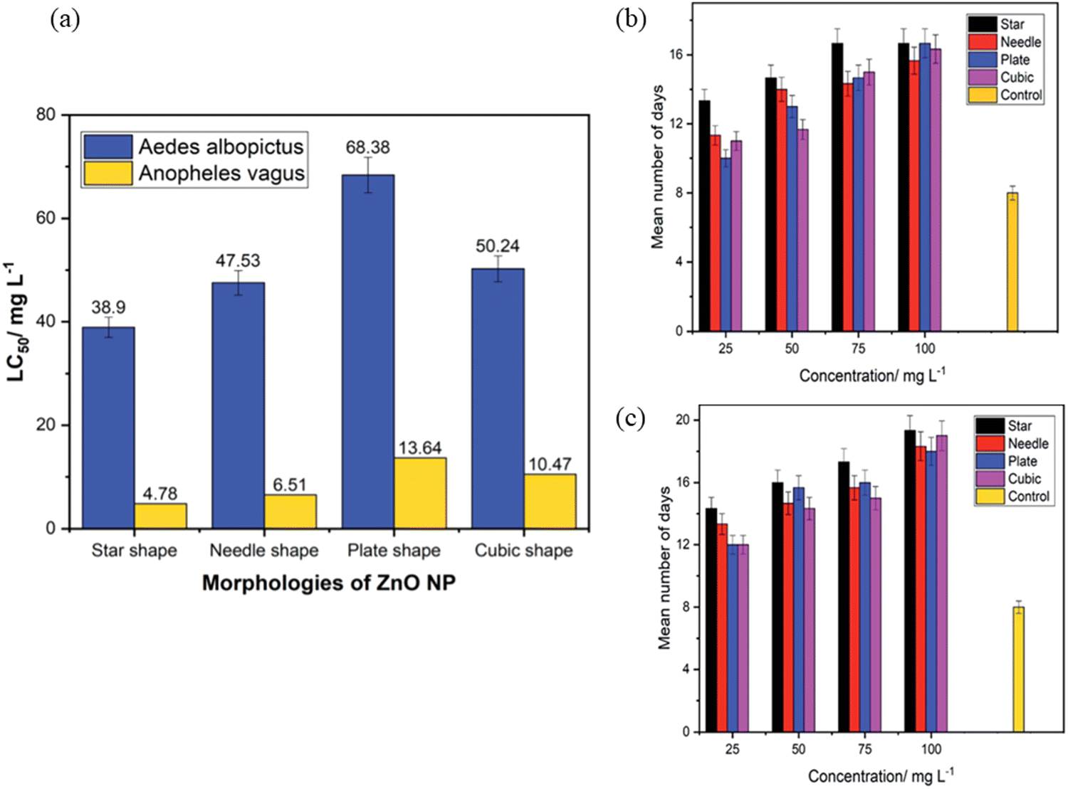 | ||
| Fig. 14 (a) The LC50 values against the larvae of Aedes albopictus and Anopheles vagus mosquitoes obtained from the four different morphologies of ZnO nanoparticles. (b and c) Number of days needed by the mosquito larvae to complete the life cycle under exposure to various morphologies and concentrations of ZnO nanoparticles. (b) Aedes albopictus, (c) Anopheles vagus. Reprinted with permission from ref. 239. Copyright 2021 Royal Society of Chemistry. | ||
Similarly, Dhavan et al.240 analyzed ZnO nanorods synthesized by green method to evaluate the larvicidal activity against the dengue vector. The LC50 value of 24.74 μg ml−1 proved that the rod-like morphology is also effective against Aedes aegypti. One of the mosquito larvae, Culex tritaeniorhynchus, extracts blood from humans as well as animals. The efficacy of ZnO NPs was studied against this larva by Velsankar et al.241 The results indicate that the mortality rate was initiated at 12 h for 40 ppm concentration of NPs. The great larvicidal activity was noticed at the lowest concentration of ZnO. It has been reported that ZnO NPs are accumulated and deposited in different parts of the larval body, such as the respiratory region, causing suffocation, and the alimentary canal, causing tissue layer damage. Zn2+ ions also hinder the growth of larvae.
4.3 Anticancer activity of ZnO nanostructures
Cancer, the abnormal growth of tissues, caused the death of around 10 million people in 2020. The most common cancers include lung cancer (1.80 million), colon and rectum (935 K), liver (830 K), stomach (769 K) and breast cancer (685 K), as per recent projections by the World Health Organization (WHO) (https://www.who.int/news-room/fact-sheets/detail/cancer). Traditional approaches, such as chemotherapy and radiotherapy, possess substantial side effects such as immunosuppression. They also affect normal cells, cause anemia, or in even more severe cases, lead to death. To overcome such drawbacks, nanotechnology plays a very crucial role. ZnO NPs are not only effective against cancer diagnosis, but they show efficacy against cancer cells. ZnO NPs have been reported to produce ROS upon contact with the cells, causing cell death to cancer tissues. It has been shown that ZnO NPs obtained from plant- and microbes-mediated synthesis show good anticancer activities. Moghaddam et al.242 affirmed that ZnO NPs obtained from a new strain of yeast, P. kudriavzevii, have powerful efficacy against breast cancer cells. The viability of the cancer cells was concentration-dependent, and decreased with increasing ZnO NPs concentration. The value of IC50 for ZnO NPs at 24 h was estimated to be 121 μg ml−1. The authors claimed that the loss of viability occurs by inducing sub-G1 phase apoptosis, and upregulating pro-apoptotic genes, e.g., p21, p53, JNK, Bax, and downregulating anti-apoptotic genes like Bcl-2, ERK1/2 and AKT1. Similarly, fabricated ZnO NPs from P. Chrysogenum demonstrated anticancer activity against breast and colon cancers. The authors reported that on irradiating the NPs with gamma radiation, the performance against the cancer cells increased.243 Recently, Zhang et al.244 studied the cytotoxic effect of ZnO NPs against human bladder cancer cell lines, T24. At low NPs concentrations, 15 μg ml−1, ZnO did not show any substantial effect after 48 h of exposure, as shown in Fig. 15. When confocal microscopy was used to investigate the level of zinc ion, green fluorescence was observed to increase with increasing NPs concentration. The NPs concentration of 10 μg ml−1 exhibited higher fluorescence intensity than that at 5 μg ml−1 (Fig. 15(b)). Upon further investigation, it was confirmed that a low dose of ZnO NPs induces S phase arrest and late apoptosis in T24 cells. In addition, it inhibited cellular migration and aggressive capacity because of the histone methylation change. The plausible mechanism of ZnO at low concentration in restraining bladder cancer proliferation and migration in T24 cells is shown in Fig. 15(c).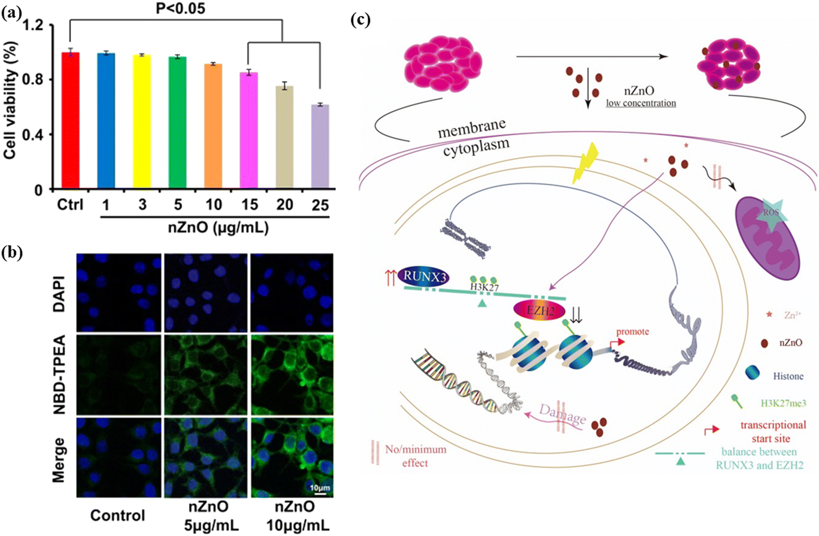 | ||
| Fig. 15 (a) Zinc detection and cytotoxicity assessment in T24 cells by ZnO NPs treatment. (b) Confocal images [NBD-TPEA (green) and DAPI (blue) staining] for the intracellular zinc ion in T24 cells upon ZnO NPs exposure for 2 days. (c) A schematic image shows the epigenetic mechanism underlying the n-ZnO-mediated anticancer effect in T24 cells. Reprinted with permission from ref. 244. Copyright 2020 Dove Press. | ||
4.4 Antimicrobial action of SnO2 nanostructures
SnO2 nanostructures exhibit antimicrobial property against a wide range of microbes, such as bacteria (both Gram-positive and -negative), viruses, and fungi, owing to their large surface area. The antimicrobial action of the nanostructures depends on a number of factors: (i) synthesis route, (ii) morphology of NPs, (iii) particle size of NPs, (iv) concentration of NPs and (v) nature of the capping agent, if used while fabricating NPs. It has been reported in the literature that SnO2 nanostructures fabricated through green methods are much preferred for their antimicrobial activities.245 Briefly, green methods utilize plant-, bacteria-, and protein-extracts to synthesize different morphologies of nanoparticles (NPs). Through this method, stable and high yield products are produced, and the starting materials are eco-friendly and biocompatible.228 Thus, the obtained nanostructures from this way are more biocompatible to be used for biological applications. Moreover, the extract used for green synthesis acts as a capping/stabilizing agent, leading to the prevention of aggregation, and therefore improves the biological potential of NPs.246 Vidhu and his team247 fabricated SnO2 nanoparticles by Saraca indica flowers, and showed their antibacterial activity against E. coli bacteria. The authors revealed that the plausible mechanism behind the antibacterial action is the generation of reactive oxygen species (ROS) NPs. The produced ROS interact with the bacterial cell membrane and penetrate the cell, as shown in Fig. 16. This results in bacterial cell death. In another study by Ayeshamariam et al.,248 synthesized SnO2 NPs by Aloe Vera plant extract were observed to be effective against both Gram-positive (S. aureus, S. typhi, S. pyogenes) and Gram-negative (E. coli and P. aeruginosa) bacteria, as analyzed via well diffusion method. The zone of inhibition (ZOI) was calculated by measuring the diameter of the inhibition zone around the well, including the well diameter. A greater value of ZOI indicates effective inhibition property. The authors reported on 100% and 75.9% activity against Gram-negative and Gram-positive isolates, respectively. The reason behind this was the presence of an Anthraquinones component possessing antimicrobial activity, as mentioned by the authors. Vidhu et al.247 also revealed that as the concentration of NPs increased, the bactericidal effect was also enhanced.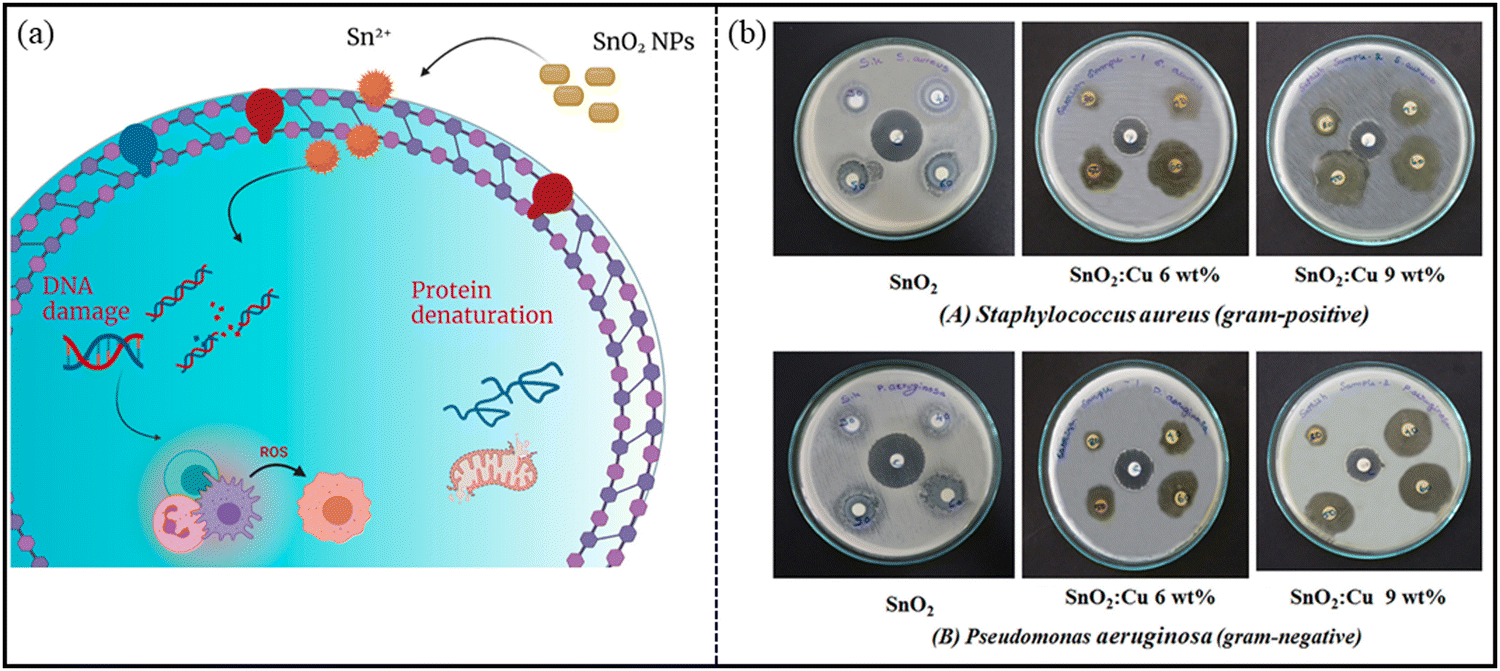 | ||
| Fig. 16 (a) Possible mechanism of the antibacterial action of SnO2 NPs. Reprinted with permission from ref. 251. Copyright 2021 MDPI. (b) Antibacterial activity of the pure and Cu-doped SnO2 NPs: (a) SnO2, (b) SnO2:Cu, 6 wt%, (c) SnO2:Cu, 9 wt%. Reprinted with permission from ref. 250. Copyright 2020 Elsevier. | ||
It has also been reported in the literature that transition metal ions-doped SnO2 show potent antimicrobial activity, such as Co-doped, Ag-doped, Ce-doped, Cu-doped SnO2 NPs. Bhawna et al.249 reported on the activity of cerium (Ce)-doped SnO2 NPs against E. coli bacteria. At low concentrations of 0.25–3 mg of NPs, no antibacterial activity was observed. However, on increasing the concentration to 4–5 mg, the antibacterial activities were analyzed by estimating the diameter of ZOI. Similarly, Sathishkumar et al.250 reported on the enhanced antibacterial activity of Cu-doped SnO2 NPs compared to pure SnO2 NPs, as revealed by calculating the ZOI (Fig. 16(b)). The authors claimed that less inhibition zone in the case of SnO2 NPs was probably due to the greater particle size and low release of Sn4+ ions, generating less ROS. On increasing the Cu dopant concentration, the diameter of the inhibition zone increased against both types of bacteria (P. aeruginosa and S. aureus) because of the improved rate of generation of Cu2+ ions and Sn4+ ions, as well as larger surface area.
Khan et al.252 analyzed the impact of green synthesized un-doped SnO2 NPs, Co-doped SnO2 NPs and plant extract on the viability of bacterial strains such as E. coli and B. subtilis via confocal and electron microscopy. Confocal micrographs (Fig. 17(a)) show the dead and live bacterial cells in red and green color, respectively. The results indicated that when bacterial cells were exposed to Co-doped SnO2 NPs, they were observed to be 100% dead compared to the untreated bacterial cells treated with plant extract and un-doped SnO2 NPs. Co-doped SnO2 NPs demonstrated almost 99% red fluorescence, confirming dead cells as shown in (Fig. 17(b)). The results were found to be in agreement with SEM (Fig. 17ii) and TEM micrographs (Fig. 17(c)). In the control samples of E. coli and B. subtilis, the morphology of these bacteria is very distinct and continuous. However, their morphologies were observed to be disordered when these bacterial cells were treated with plant extract and un-doped SnO2 NPs. The authors also observed that the bacterial membrane disruption was higher when treated with Co-doped SnO2 NPs than when treated with plant extract and SnO2 NPs, as revealed by SEM and TEM. Significant and extraordinary cell death of the bacteria was noticed by the Co-doped SnO2 NPs.
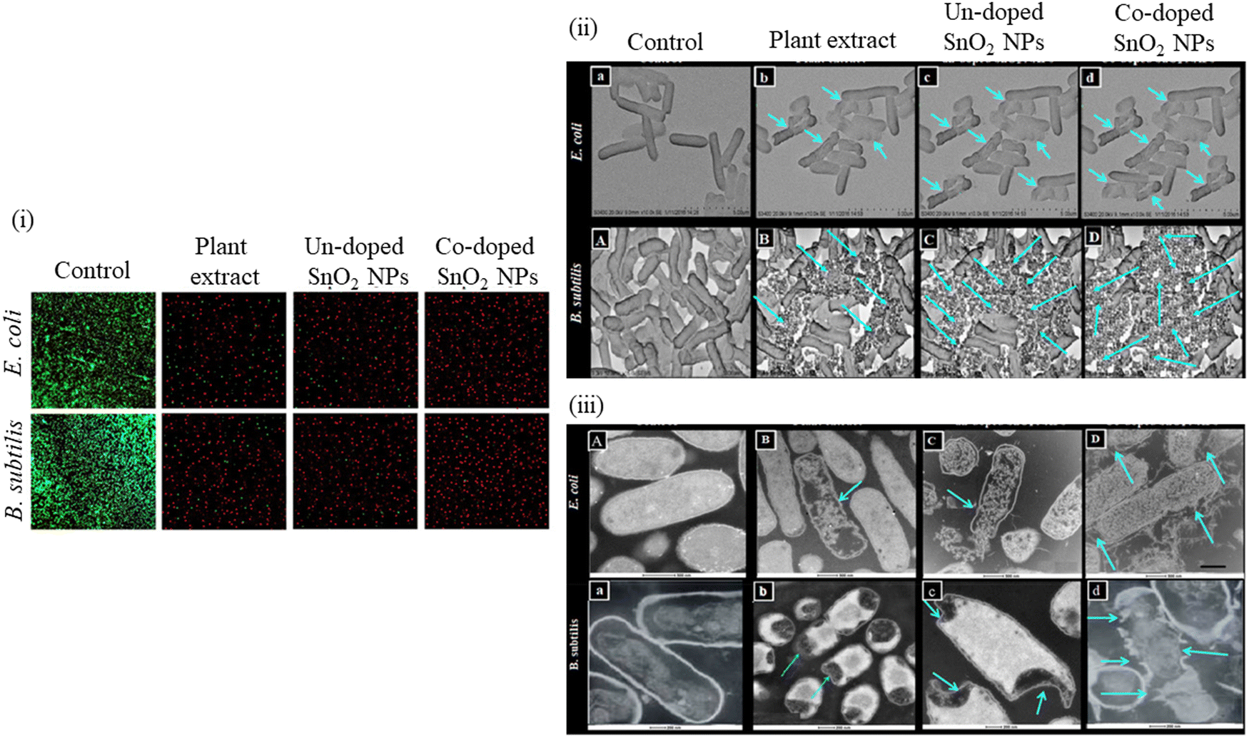 | ||
| Fig. 17 The measured confocal images (i), produced by the control and treated E. coli and B. subtilis with plant extract, green synthesized un-doped SnO2 NPs and co-doped SnO2 NPs. Morphology of the untreated and treated E. coli and B. subtilis cell strains. TEM images (ii, iii) of the untreated and treated E. coli and B. subtilis strains, i.e., control, plant extract, un-doped SnO2 NPs and Co-doped SnO2 NPs (A–D) and (a–d), respectively. Reprinted with permission from ref. 252. Copyright 2018 Elsevier. | ||
In addition to being effective against bacteria, Co-doped SnO2 NPs synthesized by green route were found to be effective against different fungal strains, such as A. flavus, A. niger, and C. albicans, with a high ZOIs of 23 ± 0.08 mm, 17 ± 0.04 mm, and 26 ± 0.06 mm, respectively. The authors suggested that its effectiveness was due to the Co doping, greater grain size and surface area, and thus more antifungal propensity.252 Similarly, in another report by Ayeshamariam et al.,248 SnO2 NPs of around 100 nm size showed antifungal activity for A. niger and M. indicus. The SnO2 nanostructures are observed to be effective as antiviral agents. Trigilio et al.253 demonstrated the antiviral activity of SnO2 nanowires, with the length varying from a few mm to 1 cm, and the diameters ranging from a few nm to the mm scale. These nanowires act like a natural target by showing an ability to compete for the virus at the attachment step. The authors reported that at the concentration of 500 and 1000 μg ml−1, the Herpes simplex virus type 1 (HSV-1) entry was 5 times lower than untreated cells.
4.5 Antioxidant activity of SnO2 nanostructures
Antioxidants play a very important role in protecting the human body from free radical damage. Actually, when biomolecules present in the human body interact with oxygen, they produce free radicals. Free radicals cause degradation to biomolecules. Thus, the function of antioxidants is to scavenge the free radicals, thereby terminating the oxidative harm to the human body. SnO2 NPs show good antioxidant property by scavenging 1,1-diphenyl-2-picrylhy-drazyl (DPPH) free radicals. Generally, the antioxidant capacity is enhanced with the increase in the concentration of SnO2 NPs. Hong et al.254 determined the inhibition of DPPH free radicals by SnO2 NPs synthesized by means of Litsea cubeba fruit extract, with the half maximal inhibitory concentration (IC50) value to be 2257.4 μg ml−1. The authors suggested that the antioxidant property was stronger in the sample without annealing because the FTIR study revealed that the antioxidant components were adsorbed on the NPs surface in the unannealed sample. Kamaraj et al.255 investigated the antioxidant action of SnO2 NPs obtained using Cleistanthus collinus. The authors noticed that with the increase in concentration and time, the antioxidant activity also was enhance. Similarly, Vidhu et al.247 confirmed that the % of the free radical scavenging action increases with an increase in the concentration of NPs, as represented in Fig. 18(a). Khan et al. determined the free radical scavenging property of the un-doped, Co-doped SnO2 NPs and plant extract, considering butylated hydroxytoluene (BHT) as standard, as shown in Fig. 18(b). The maximum and significant DPPH radical scavenging ability of Co-doped SnO2 NPs was 40, 59, 78 and 88% at different concentrations of 25, 50, 75 and 100 μg ml−1, respectively.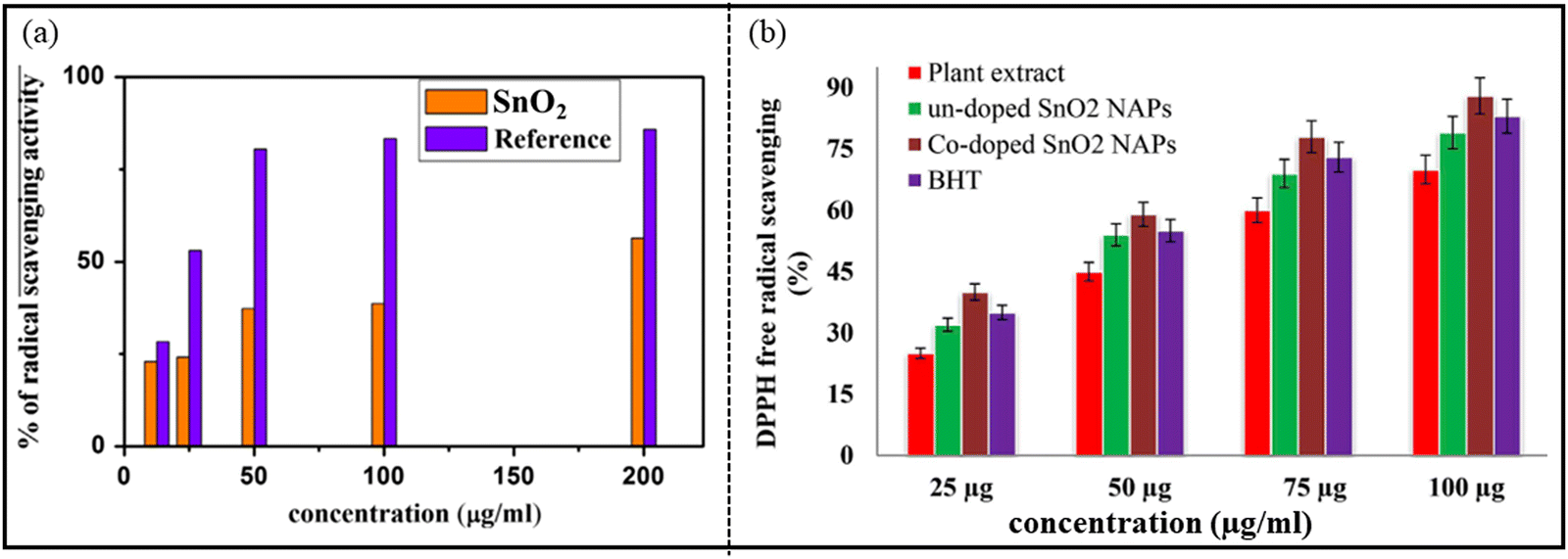 | ||
| Fig. 18 Antioxidant activity using DPPH assay: (a) SnO2 NPs. Reprinted with permission from ref. 247. Copyright 2015 Elsevier. (b) Plant extract, green synthesized un-doped SnO2 and Co-doped SnO2 NPs, employing BHT as an external standard. Reprinted with permission from ref. 252. Copyright 2018 Elsevier. | ||
Nanocomposites of SnO2 with noble metals such as Ag display good efficacy against free radicals with an IC50 value of 0.73 mM taking Quercetin as a standard antioxidant, as elucidated by Sinha et al.256 However, the authors did not report on any insight mechanism to support the results.
4.6 Anticancer activity of SnO2 nanostructures
As per the literature, SnO2 nanostructures are well known for their anticancer activity. Khan et al.252 synthesized SnO2 NPs and Co-doped SnO2 NPs by green methods, utilizing the Clerodendrum inerme extract. The obtained NPs were evaluated for their anticancer propensity against mammary gland breast cancer (MCF-7) cell lines. At different concentrations of 25, 50, 75 and 100 μg ml−1, Co-doped SnO2 NPs were observed to exhibit considerable mortality rate compared to the un-doped SnO2 NPs. The IC50 value after 48 h of incubation (vs. the control) for the Co-doped SnO2 NPs was 18.15 ± 1.0 μg ml−1 compared to 31.56 ± 1.4 μg ml−1 and 26.99 ± 1.9 μg ml−1 for the plant extract and un-doped SnO2 NPs, respectively. In another report by Li et al.,257 the authors found that SnO2 NPs of particle size 27.45 ± 13.4 nm exerted a cytotoxic effect on the human oral cancer cell line, CAL-27. Compared to the control, the SnO2 NPs (50, 100, 200 μg ml−1) (all P < 0.05) exhibited a significant decrease in the proliferation activity of the cancer cells. The cell inhibition was noticed to be higher at 48 h than at 24 h. At the concentration of <50 μg ml−1, no substantial cell proliferation was analysed (all P > 0.05). In addition, nanoporous materials are currently attracting attention because the mesoporous nanomaterials can penetrate the irregular vascular structure of tumor tissues, and thus enhance the antitumor effect and reduce the associated side effects. Lv et al.258 synthesized mesoporous folate-functionalized SnO2 nanofibers and analyzed their effects on tumor cells. The average outer diameter of the obtained nanofibers was estimated to be 200 nm, and the wall thickness was 50 nm. In vitro and in vivo experiments revealed that the nanofibers could significantly inhibit the growth of SMMC-7721 cells.Multifunctional ZnO/SiO2 core/shell nanoparticles for bioimaging and drug delivery application have also been reported by G. D. Venkatasubbu and his team. Due to their biocompatibility and low cost, ZnO nanoparticles have been used for the bioimaging and drug delivery application. ZnO nanoparticles were prepared by the co-precipitation method, and the ZnO/SiO2 core/shell nanoparticles were developed (Fig. 19a–d). The drug release profile of the curcumin-loaded ZnO/SiO2 core/shell nanoparticles was reported. It was found that the high surface area and low toxicity make ZnO/SiO2 an appropriate material for drug delivery applications, where the drug is attached to the surface of the silica shell due to hydrogen bonding and electrostatic interaction, and a sustained drug release of 80% of the drug occurs within 24 h with an obtained variance of P < 0.001.259
 | ||
| Fig. 19 (a and b) HRTEM image of the ZnO/SnO core shell nanoparticles. (c) Drug release profile of the curcumin-loaded ZnO/SnO2 core shell structure, and (d) hemolysis percentage of the pure and ZnO/SnO2 core shell nanoparticles. Reprinted with permission from ref. 259. Copyright 2020 Springer Nature. | ||
5. Piezoelectric nanogenerator for energy harvesting
5.1 ZnO-based piezoelectric nanogenerator
Piezoelectric nanogenerators have been proven as emerging nanodevices to harvest the mechanical energy from various sources, including air flow, vibration, rain drop, walking, and blood flow.260–262 Semiconducting piezoelectric ZnO nanostructures exhibit superior properties over other piezoelectric nanomaterials due to the easy fabrication of piezoelectric diodes, piezophotonics, and piezophototronics devices. The 1D piezoelectric ZnO nanostructures have been utilized for flexible piezoelectric nanogenerators, Schottky contact-based nanosensors, and self-powered piezotronics strain sensors.263–270In 2006, vertically aligned zinc oxide nanowire arrays were used as piezoelectric active materials by Z. L. Wang and his team, and they successfully demonstrated the energy-harvesting application using atomic force microscopy. They measured the output voltage by AFM technique using a Pt-coated Si tip with a cone angle of 70° (Fig. 20). They successfully demonstrated the creation of a strain field via coupling the semiconducting and piezoelectric properties of zinc oxide NWs. The efficiency of the power generator based on the piezoelectric property of zinc oxide was reported to be in the range of 17–30%.271
 | ||
| Fig. 20 (a and b) TEM image of the vertically aligned ZnO nanowires. (c) Schematic of the AFM measurement of single ZnO nanowires for piezoelectric measurements. Reprinted with permission from ref. 271. Copyright 2006 The American Association for the Advancement of Science. | ||
Gupta et al. fabricated vanadium (V) doped ZnO nanosheets (NS) to enhance the piezoelectric properties of pristine ZnO nanostructures.272 They reported that by vanadium doping, the nanorods-like morphology was transformed into nanosheets. It was reported that with the shielding effect and presence of the OH-ions, the nanorods were converted into nanosheet structures. The V-doped ZnO nanosheets show a d33 value of 4 pm V−1, measured through the PFM technique. They reported that the piezoelectricity of the V-doped ZnO nanosheets was greatly improved, which is due to the generation of a large polarization in the V-doped ZnO NS originating from the rotation of the Zn–O bonds and V–O bonds. The high piezoelectric constant is also due to the noncollinear V–O bonds, which has stronger polarity than the Zn–O bonds and can rotate easily under an electric field. A high-performance piezoelectric nanogenerator was fabricated using the flexible ITO-coated PET substrate. The authors reported that the V-doped ZnO nanosheets-based device under a vertical compressive force of 0.5 kgf generates a DC-type current of 1.0 μA cm−2, while the ZnO nanorods generates an AC-type signal of ∼10 nA cm2 under the same condition (Fig. 21). They confirmed that the output performance increased due to the network structure of the ZnO nanosheets.272 K. Y. Lee et al. also developed a piezoelectric nanogenerator based on one-dimensional zinc oxide (ZnO) nanowires (NWs). They improved the output performance of the ZnO NWs-based nanogenerator by controlling the energy band at the depletion width through a p-type semiconductor polymer and native defects. The authors synthesized the vertically aligned flexible ZnO nanowires on the ITO-PEN substrate using the seed-assisted solution technique. A p-type P3HT polymer-coating over the ZnO nanowires was used to increase the performance of the energy-harvesting device. The output performance was increased several times compared to the output voltage of the pristine ZnO NWs-based nanogenerator (Fig. 22). Due to the p-type nature and presence of the holes, drastically decreases the piezoelectric screening effect caused by the ZnO free electrons, the resulting output voltage improved.273
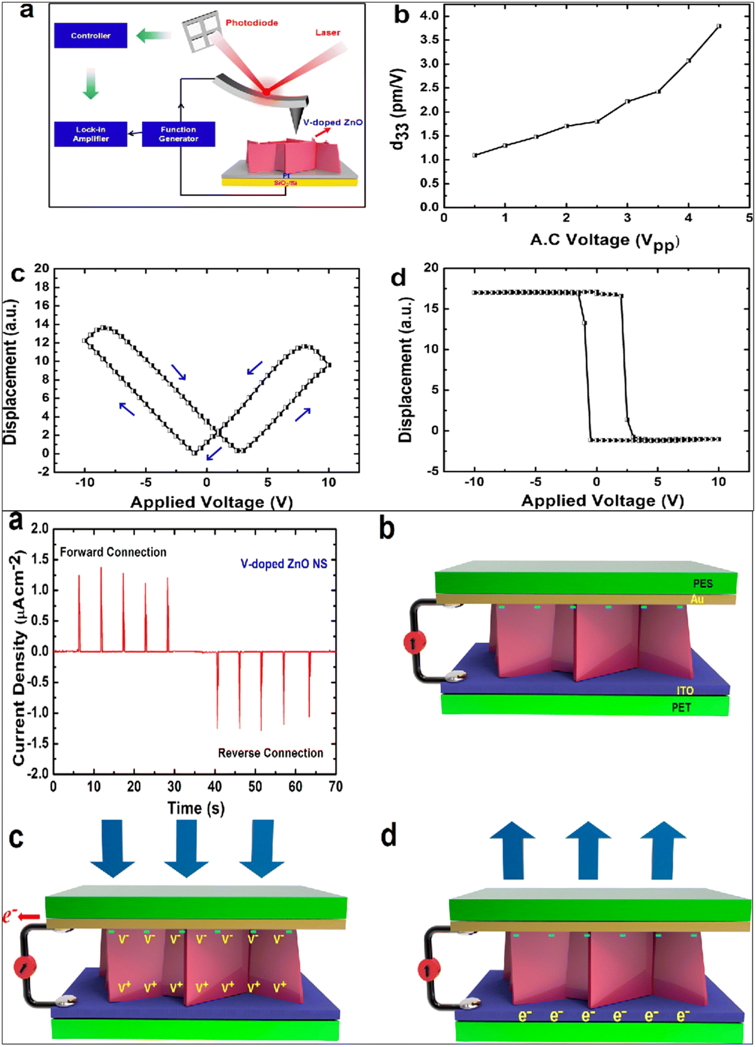 | ||
| Fig. 21 (a) Experimental diagram of the piezoelectric response (d33) measurement through the PFM setup. (b–d) Butterfly curve and phase-voltage hysteresis curve. (e) The current density obtained from the V-doped ZnO nanosheets showing DC-type charge generation. Mechanism of charge generation of the V-doped ZnO device. Reprinted with permission from ref. 272. Copyright 2013 American Chemical Society. | ||
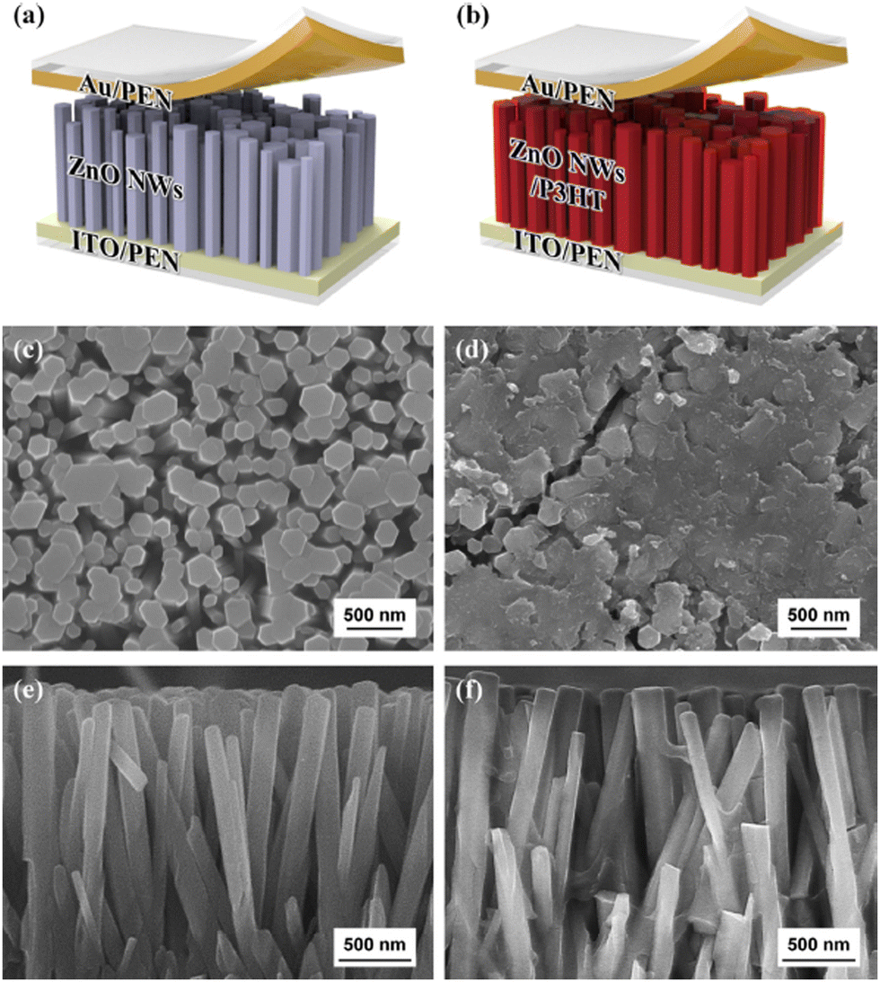 | ||
| Fig. 22 (a) Schematic image of the pristine ZnO NWs nanogenerator and (b) P3HT-ZnO NWs-nanogenerator. (c) Top view morphology of the pristine ZnO NW and (d) P3HT-coated ZnO NWs. (e and f) Cross-sectional morphology images of the ZnO NWs and P3HT-ZnO NW. Reprinted with permission from ref. 273. Copyright 2014 Elsevier. | ||
K.-H. Kim et al. reported on the pristine 2D zinc oxide nanosheets and anionic nanoclay layer-based nanogenerator for scavenging mechanical energy. They successfully demonstrated the collective effect of the semiconducting, piezoelectric, buckling property of ZnO NS on the performance of the nanogenerator, and an efficient DC-type output power voltage was obtained. Several electrodes (Au, graphene, indium tin oxide (ITO), and Al) were used to investigate the performance of the ZnO-based nanogenerator. The output performance of the nanosheet nanogenerator was measured using a force simulator. The output voltage and output current density were about 0.44 V and 6.5 μA cm−2, respectively, under 1 kgf. They reported that the output performances of the voltage and current were higher in the case of the Au top electrode, as compared to the graphene, ITO and Al top electrode (Fig. 23). The results also indicated that the nanosheets-like morphology is preferable over the nanorods-like morphology due to the enhanced mechanical properties, especially for nanogenerator applications.274
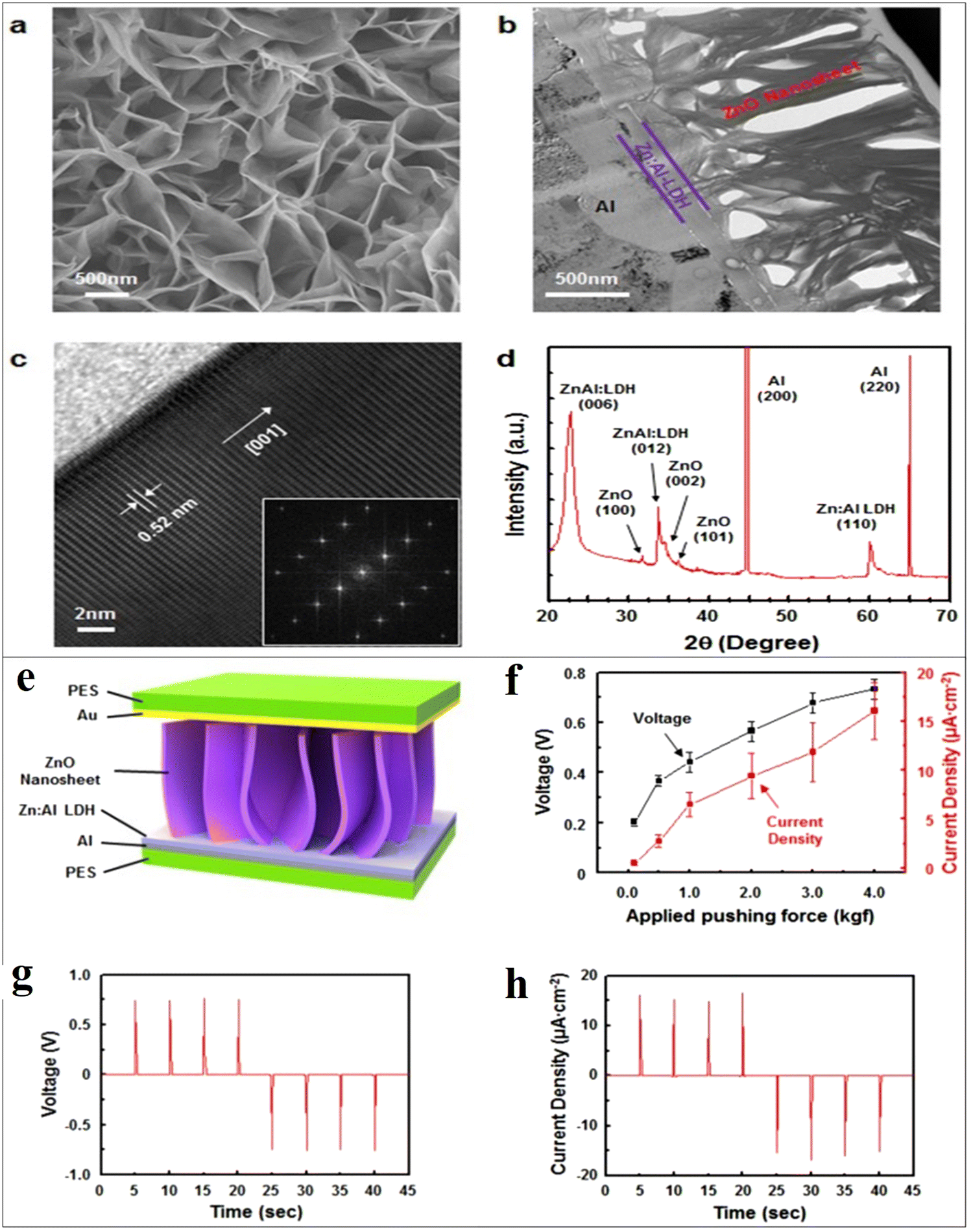 | ||
| Fig. 23 (a) Morphology of the ZnO nanosheets network structure grown on an Al substrate. (b) TEM (cross-sectional image) of the ZnO nanosheets network. (c) HR TEM image and corresponding FFT pattern (inset). (d) Synchrotron XRD pattern of the ZnO nanosheets (e–g). Schematic image and output voltage from the ZnO nanosheet-based nanogenerator. (h) Measured current density of the ZnO nanosheet-based nanogenerator. Reprinted with permission from ref. 277. Copyright 2013 Springer Nature. | ||
It has been shown that morphological changes greatly affected the output performance of the piezoelectric nanogenerator due to the high surface-to-volume ratio and good mechanical durability. The change in the output performance was due to the change in the piezoelectric polarization and piezoelectric charge coefficient. Gupta et al. showed that the V-doping morphology of the ZnO nanorods (1D) converted them into ZnO nanosheets (2D). This was due to the crystallographic growth shielding effect on the c-axis and preferred growth along the a-axis of ZnO, which was caused by the formation of V(OH) ions on the positively charged (0001) Zn-terminated surface, enabling an enhanced DC type current output to be obtained. The occurrence of the DC type electric signal, rather than an AC type electric signal, from the 2D ZnO nanosheets is due to the presence of OH− ions. Owing to the anisotropic crystal property of the ZnO nanosheets, the effect of the direction of the force, magnitude of the force, and the bending degree on the piezo-potential of the nanogenerator have been reported by Ang Yang and his team. They reported that the 2D structures show high durability due to the interconnected structures. The 2D structures tolerate relatively large deformations prior to fractures, demonstrating the high stability of the material.275–277
5.2 Tin Oxide (SnO2):PVDF and SnO2/ZnO-based piezoelectric nanogenerators
Tin oxide (SnO2) exhibits a large band gap n-type semiconductor nature, which then makes it suitable for various technological applications in various fields, including infrared detectors, solid state gas sensors, photodetectors optical devices, and heat reflecting mirrors.278–281 The piezoelectric properties of the pristine SnO2-based nanostructures are rarely reported. The SnO2 nanostructures were recently reported as reinforcement materials to fabricate a piezoelectric nanocomposite nanogenerator. The 2D-based SnO2 nanosheet/PVDF composites-based piezoelectric nanogenerator was fabricated by E. Kar et al.282 The ultrathin 2D SnO2 nanosheets were grown by hydrothermal method. They fabricated the SnO2NS/PVDF nanocomposite-based nanogenerator to convert mechanical to electrical energy. The SnO2 sheet improved the piezoelectric properties of the PVDF, and the output voltage dramatically increased. They fabricated a human body motion-based nanogenerator. The authors demonstrated that the inorganic–organic 2D SnO2 nanosheet/PVDF composite-based piezoelectric nanogenerators produced a high output voltage of 42 V and current density of 6.25 μA·cm−2 under gentle human finger tapping (Fig. 24). It was also proposed that the incorporation of homogeneously distributed 2D SnO2 nanosheets improved the performance of the self-polarized composite due to the high surface area that increased the β phase in PVDF composites. The output power was used to illuminate the 85 light emitting diodes via bridge rectifiers. The self-cleaning performance of the SnO2-PVDF nanogenerator was also demonstrated.282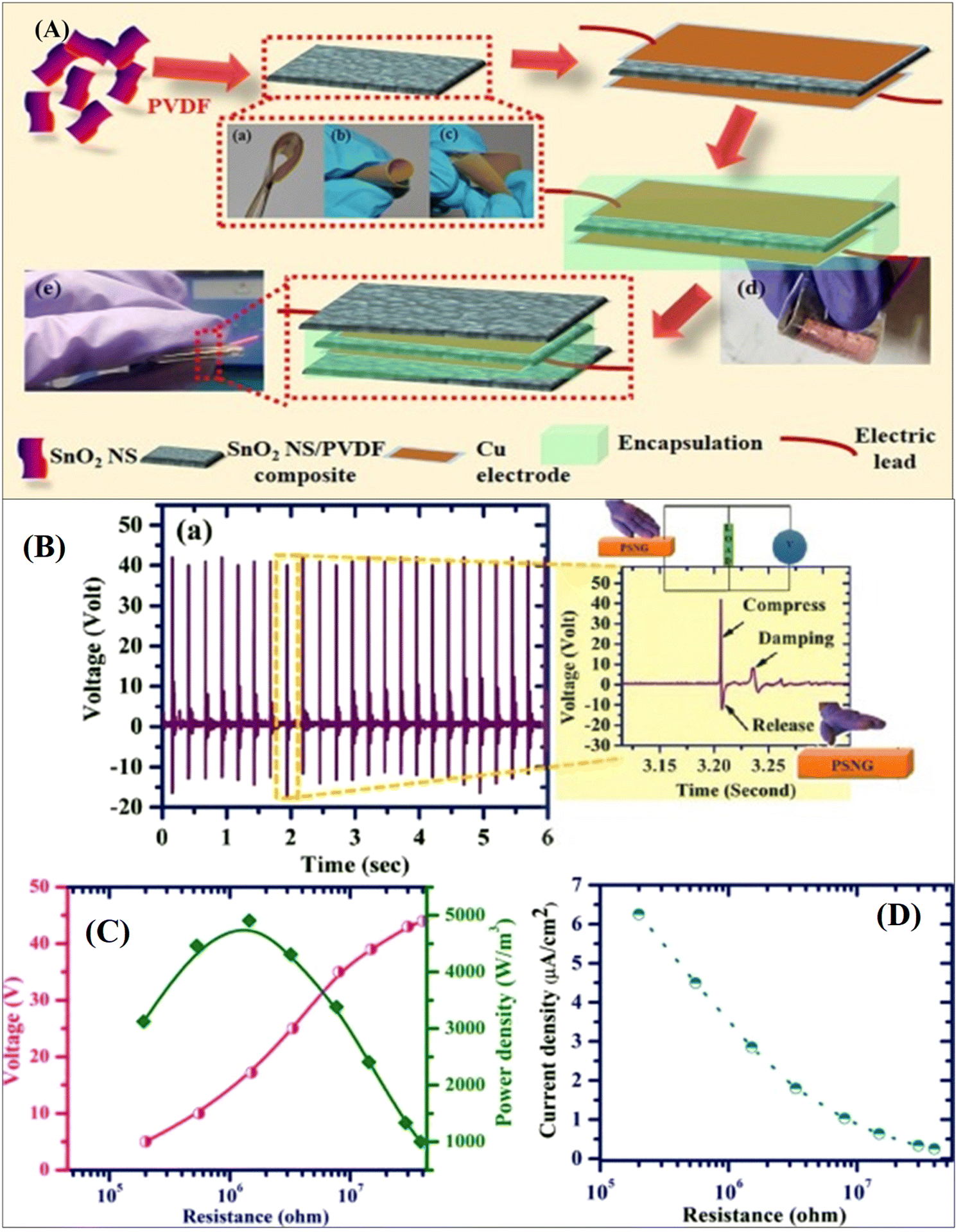 | ||
| Fig. 24 (A) Schematic image of the fabrication procedure of the SnO2NS/PVDF-based nanogenerator (a–e). (B) Output voltage produced from the SnO2NS/PVDF nanogenerator. (C) Variation of the output voltage and (D) power density with load resistance. Reprinted with permission from ref. 282. Copyright 2019 Elsevier. | ||
A humidity sensing based on the piezoactive SnO2/ZnO nanoarray-based nanogenerator with high electrical response and high detecting range was developed by D. Zhu et al.283 The SEM image of the SnO2/ZnO NW arrays revealed the uniform coating with many SnO2 nanoparticles on ZnO nanowires. The authors fabricated the piezoelectric humidity sensor device, and their device performances were measured under different humidity conditions. They demonstrated a piezoelectric output voltage of 0.55 at 5% RH, 0.50 at 25% RH, 0.33 at 45% RH, 0.25 at 55% RH, 0.21 at 65% RH, and 0.13 in a relative humidity condition of 85% from the SnO2/ZnO NW arrays-based nanogenerator (Fig. 25). The piezoelectric voltage decreased with the increase in relative humidity of the atmosphere, and the response of the hybrid SnO2/ZnO arrays as the piezo/active humidity sensor was high.283
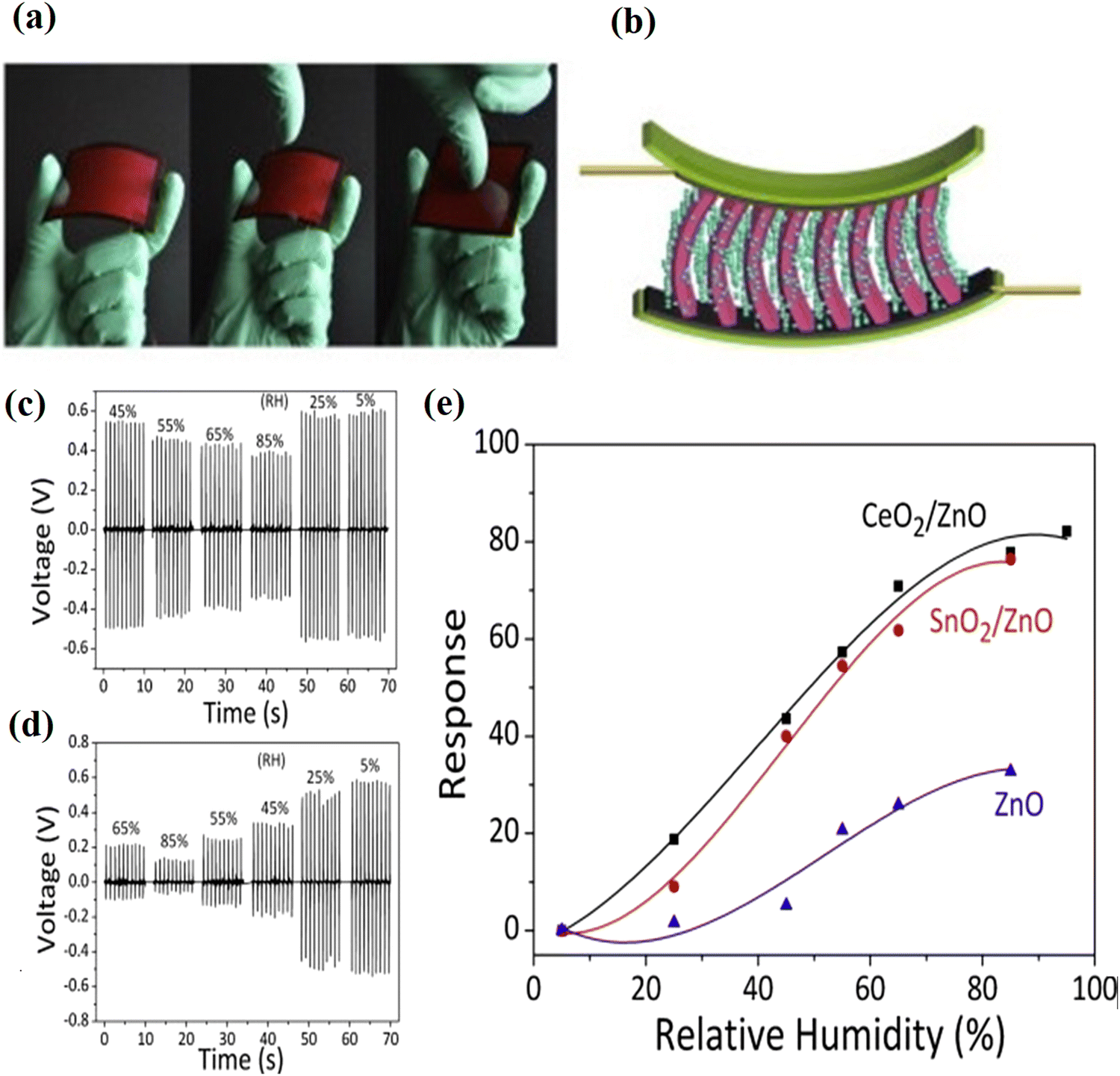 | ||
| Fig. 25 (a and b) The original picture of the ZnO/SnO2-based flexible device under compressive deformation through human fingers. (c and d) Piezoelectric output voltage signal measured under different relative humidity conditions. (e) Response of the device under different relative humidity conditions. Reprinted with permission from ref. 284. Copyright 2014 Elsevier. | ||
The piezoelectric semiconductor coupling properties of the n-type ZnO nanostructures with various morphologies were used to improve the performance of numerous devices. Such dramatic coupling behavior of the semiconducting and piezoelectric properties have recently developed the new concept of piezotronics and piezo-phototronics devices. Owing to this coupling behavior, the performance of the ZnO-based photodetector and solar cell have been tuned by the piezoelectric effect caused by mechanical deformation and interface engineering.284 Recently, J. Zhai and his team used the n-type ZnO thin film and developed a photodetector using the p-type CuI film. They have shown that by using the p-type CuI and engineering the interface between ZnO and CuI, the piezoelectric performance of the ZnO-based nanogenerator improved from 0.8 V to 5.0 V by the formation of a p-CuI/n-ZnO junction (Fig. 26). In addition, it was shown that the piezo-phototronic effect enhanced the photoresponsivity by up to 384%. The high performance is due the reduction of the screening effect due to free electrons in n-type ZnO.285 Moreover, a piezoelectric nanogenerator based on ZnO nanostructures doped with various halogen elements (fluorine, chlorine, bromine, and iodine) has also been reported by Yang Zhang et al.286
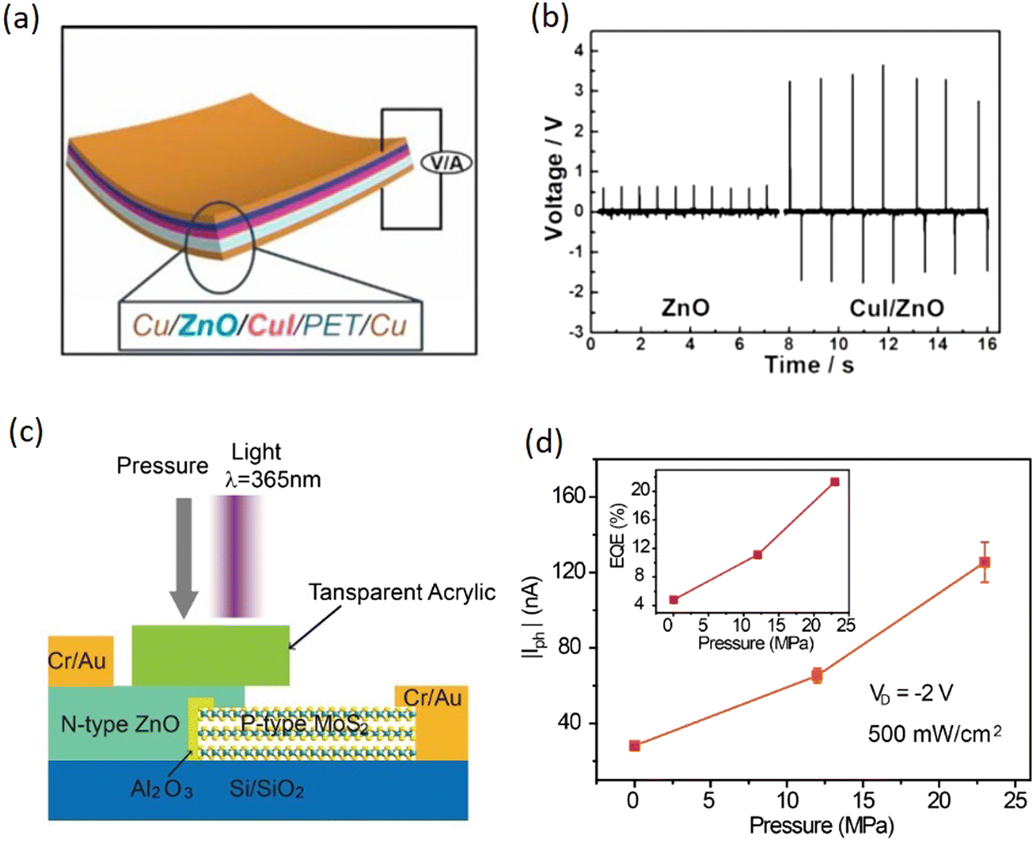 | ||
| Fig. 26 (a) Schematic presentation of the ZnO/CuI-based piezoelectric photodetector and nanogenerator (b) output voltage of the pristine and ZnO–CuI-based devices. Reprinted with permission from ref. 285. Copyright 2016 Elsevier. (c) Piezotronics device based on ZnO and MoS2. (d) Piezo-photoresponse from the piezotronics FET device. Reprinted with permission from ref. 288. Copyright 2016 John Wiley and Sons. | ||
The performance of the nanogenerator was increased by the lattice strain-induced charge separation under the compressive and tensile state along the ZnO c-axis. The piezo-photonics application of the flexible vertically aligned Li-doped ZnO nanowires-based piezotronic transistor array for in-plane strain mapping has also been reported by Z. L. Wang and his team.287 In addition, the semiconductor nanoarrays were used to established a force mapping method based on a “light nano-antenna” array using the concept of the piezo-phototronic effect. Similarly, a n-type ZnO thin film was used to fabricate the photodetector, along with the p-type MoS2 nanoflakes by Xiu et al. It was reported that the hybrid device showed an excellent rectification ratio and very strong photoresponse. An external quantum efficiency of 52.7% and a response time of 66 ms were obtained under 365 nm optical irradiation. Such improvement in the high photocurrent was obtained through the piezophototronic effect energy band modification under application of the compressive strain (Fig. 26c and d).288 The piezo-photonics application of the semiconducting nanostructures were also used for the real-time imaging of living cells traction force as performed by Q. Zheng et al. This dynamic mapping of living cells provides great insight for detecting the cardiovascular activities of the heart. A light nano-antenna array with the use of the piezo-phototronic effect has been demonstrated.289
The morphological evaluation of the ZnO semiconductor has drastically changed the device performances. Zhong Lin Wang and his team investigated the role of the 2D morphology of the semiconductor and piezoelectric ZnO on the output performance of the nanogenerators. It was also demonstrated that the 2D ZnO nanosheets-based nanogenerator showed high current density and output voltage as compared to the 1D ZnO nanorods. Recently, L. Wang et al. demonstrated the 2D piezotronics in atomically thin zinc oxide sheets. They fabricated the device based on the solution-grown 2D ZnO nanosheets. The inner crystal out-of-plane potential generated in the atomically thin ZnO surfaces under stress/strain by the piezoelectric polarization simultaneously modulates the metal-ZnO Schottky barrier height and the conductive channel width of ZnO. Therefore, the electronic transport processes in the two-terminal devices were effectively tuned by an external mechanical force. They also reported the thickness dependence of the 2D piezotronics in interfacing gating and channel width gating. Zhong Lin Wang and his team developed the ultrathin piezotronic transistors with 2-nanometer channel lengths using the ZnO nanostructure. A strain-gated FET piezotronics device was fabricated. The performance of the 2D-based device was measured under application of the pressure, and the IV characteristics were also measured. It was observed that the charge carrier transport characteristics of these devices are effectively gated by the piezoelectric polarization charges created at the Schottky metal-semiconductor interface (Fig. 27 and 28).129,130
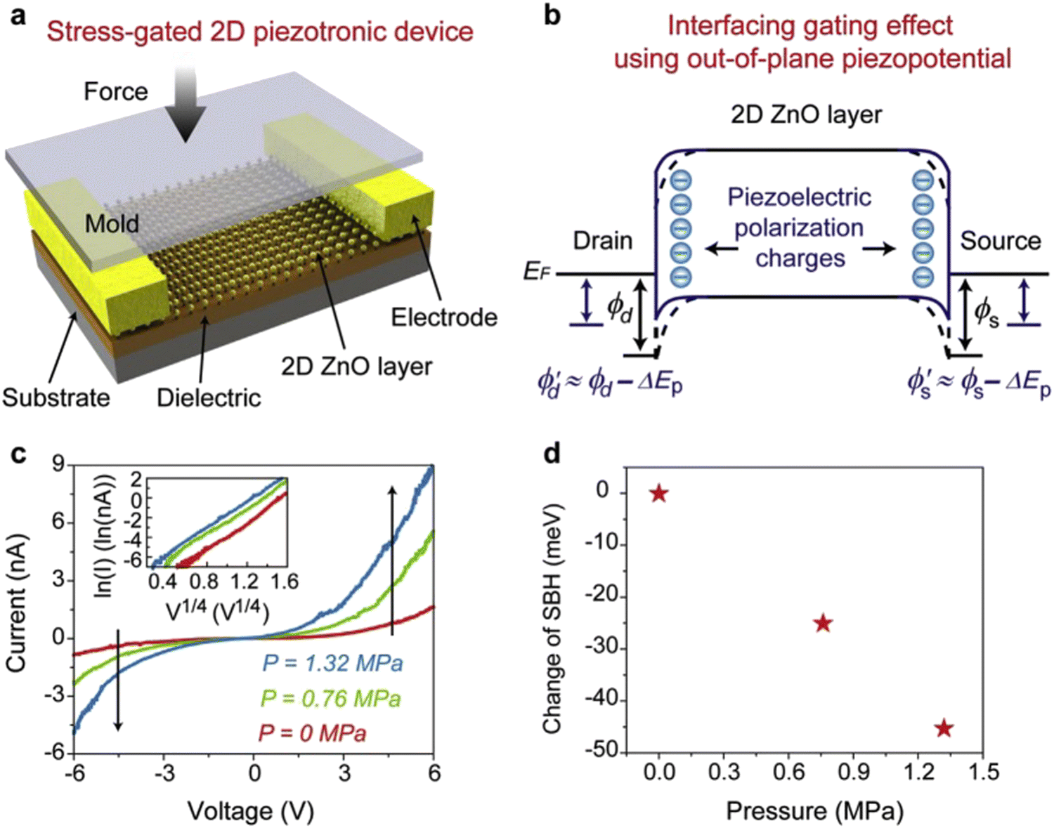 | ||
| Fig. 27 (a and b) Schematic device diagram of the stress-gated 2D layer-based piezotronics device and band diagram. (c) IV characteristic of the 2D ZnO FET piezotronics device under mechanical stress. (d) Response of the SBH with application of the pressure from the device. Reprinted with permission from ref. 129. Copyright 2019 Elsevier. | ||
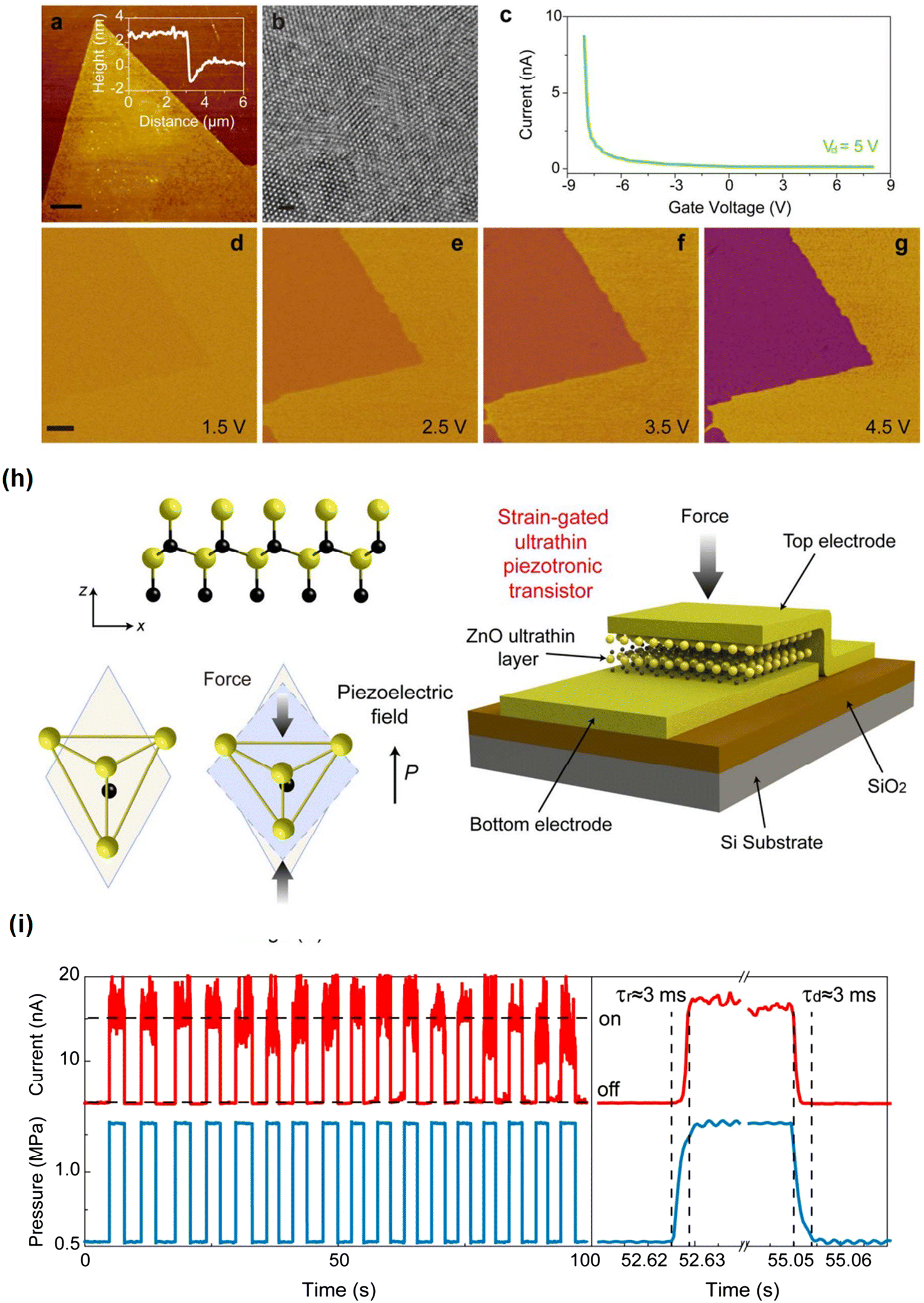 | ||
| Fig. 28 (a) AFM topography image of the ultrathin film ZnO nanosheets. (b) HRTEM image of the ZnO ultrathin film. (c) Electronic property of the ZnO ultrathin film showing the p-nature of the ZnO ultrathin film. (d–g) Amplitudes versus applied voltages (1.5–6.5 V), showing inverse piezoelectricity. (h) Schematic presentation of the ultrathin piezotronic 2D ZnO-based transistor. (i) Real-time measurement of the current through an ultrathin piezotronic transistor. Reprinted with permission from ref. 130. Copyright 2018 American Chemical Society. | ||
The output voltage and current density obtained from various piezoelectric nanogenerators based on different morphologies of the ZnO and SnO2 nanostructures are summarized in Table 1. The results showed that the change in the morphologies of the piezoelectric nanostructures led to the drastic changes in the output performances of the nanogenerators.
| S. no. | Nanostructures | Output voltage | Output current/current density | Ref. |
|---|---|---|---|---|
| 1 | V-ZnO nanosheet | — | 1.5 μA cm−2 | 272 |
| 2 | Pure ZnO nanosheet | 0.44 V | 6.5 μA cm−2 | 274 |
| 3 | SnO2/PVDF nanocomposite | 42 V | 6.25 μA cm−2 | 282 |
| 4 | SnO2/ZnO NW arrays | 0.55 V | — | 283 |
| 5 | ZnO nanostrands | 150 mV | 400 nA | 290 |
| 6 | ZnO nanorods | ∼3 V | 20 nA | 291 |
| 7 | Li-ZnO nanowires | ∼180 V | ∼50 μA | 292 |
| 8 | Sound driven ZnO nanowire | 50 mV | — | 293 |
| 9 | ZnO nanodiscs | 17 V | 150 nA | 294 |
| 10 | NiO-ZnO heterostructure | 430 mV | 40 nA cm−2 | 295 |
| 11 | Au-ZnO nanorods | 2V | 1 μA cm−2 | 296 |
| 12. | ZnO nanosheet | 0.924 V | 6 μA | 297 |
| 13 | ZnO nanowires film | 1.5 V | 25 nA | 298 |
| 14 | ZnO nanotubes | 35 mV | — | 299 |
| 15 | ZnO-polycarbonate nanocomposites | 1.15 V | 100 μA | 300 |
6. Conclusions and future outlook
This current review discussed and analyzed the recent works that addressed the synthesis of the various metal oxide nanostructures and their potential uses as solar cells, humidity sensors, and applications in biomedical and piezoelectric nanogenerators. This review has extensively discussed the effect of the morphologies of the two metal oxides, ZnO and SnO2 nanostructures, on the growth parameters and their crystal growth habits. The importance of the ZnO nanostructures, such as ZnO and SnO2 tetrapod-like morphologies, for versatile applications are discussed in detail. The surface modification of ZnO and SnO2, and the other device enhancement factors (like the particle size, concentration, morphologies, defect and charge transports) in the ZnO and SnO2 metal oxide nanostructures are summarized. The power conversion efficiencies of the flexible perovskite and dye-sensitized solar cells have a significant impact on the band gap and crystalline defects presented in the metal oxide nanostructures. Various combinations of metal oxide nanostructures with interfacial modifications have been reported to improve the performance and stability of the solar cell. Biological application of the ZnO and SnO2 nanostructures as antimicrobial agents, anticancer agents and their antilarvicidal activity are presented in the current review, as these materials exhibits unique physicochemical and structural properties, such as shape, zeta potential, crystallinity and porosity. The effective potency of the ZnO nanostructures against various viruses, including SARS-COV-2, has also been discussed. Furthermore, the review article covers the interesting applications of the ZnO nanostructures as flexible piezoelectric nanogenerators and as tiny energy-harvesting devices. The 1D and 2D ZnO nanostructures and their morphological effects on the output performance of the flexible piezoelectric nanogenerator are also addressed. In addition, this review shows that the doping, defects control and surface passivation in the metal oxide nanostructures can tailor the performance of the nanogenerator. Moreover, the application of the metal oxide SnO2 nanostructures as reinforcement materials with various polymers as a flexible nanogenerator and the effect of SnO2 on the device performance were discussed. The morphological change in the metal oxide nanomaterials can enhance the efficiency of solar cells, sensor, biological activity and output performance of the piezoelectric nanogenerators. Despite many studies and the progress that has been made so far in terms of the morphological importance of the metal oxide nanostructures, there is still much room for further growth and device performance improvements. The major challenges that need to be controlled are the various types of native defects in the nanostructures to achieve their superior applications in the sensors and solar cells. With a strong interfacial bonding and their ability to bind with the various viruses, antibodies with the nanostructure surfaces are among the critical parameters that need to be enhanced. Moreover, in terms of increasing the performance of the piezoelectric nanostructures-based nanogenerator, especially for the output current density, the interfaces of the top and bottom electrodes with optimized work functions need to be more effective than the present progress. Moreover, the integration of the ZnO and SnO2 nanostructures with the polymer and their dispersion also need to improve. Overall, the coupling of the piezoelectric nanogenerator along with the solar cell system and biosensors has lead to the creation and design of a new and sustainable efficient hybrid solar-mechanical energy harvester system and the fabrication of self-powered biomedical applications.Conflicts of interest
The authors declare that there is no conflict of interest.Acknowledgements
Manoj Kumar Gupta is thankful to CSIR, India for the CSIR-Young Scientist Award (OLP-201) and CSIR Raman Research Fellowship.References
- C. Buzea, I. I. Pacheco and K. Robbie, Biointerphases, 2007, 2, MR17–MR71 CrossRef PubMed.
- D. Agarwal, C. O. Aspetti, M. Cargnello, M. Ren, J. Yoo, C. B. Murray and R. Agarwal, Nano Lett., 2017, 17, 1839–1845 CrossRef CAS PubMed.
- E. Roduner, Chem. Soc. Rev., 2006, 35, 583–592 RSC.
- R. F. Service, Science, 2001, 293, 782 CrossRef CAS PubMed.
- D. Agarwal, M.-L. Ren, J. S. Berger, J. Yoo, A. Pan and R. Agarwal, Nano Lett., 2019, 19, 1204–1209 CrossRef CAS PubMed.
- J. N. Tiwari, R. N. Tiwari and K. S. Kim, Prog. Mater. Sci., 2012, 57, 724–803 CrossRef CAS.
- A. Glezer, Russ. Metall. Fuels, 2011, 4, 263–269 CrossRef.
- P. C. Ray, Chem. Rev., 2010, 110, 5332–5365 CrossRef CAS PubMed.
- K. L. Kelly, E. Coronado, L. L. Zhao and G. C. Schatz, J. Phys. Chem. B, 2003, 107, 668–677 CrossRef CAS.
- K.-S. Lee and M. A. El-Sayed, J. Phy. Chem. B, 2006, 110, 19220–19225 CrossRef CAS PubMed.
- C. J. Murphy, T. K. Sau, A. M. Gole, C. J. Orendorff, J. Gao, L. Gou, S. E. Hunyadi and T. Li, J. Phys. Chem. B, 2005, 109, 13857–13870 CrossRef CAS PubMed.
- D. Agarwal, J. Yoo, A. Pan and R. Agarwal, Nano Lett., 2019, 19, 7950–7956 CrossRef CAS PubMed.
- X. Hu, J. Gong, L. Zhang and J. C. Yu, Adv. Mater., 2008, 20, 4845–4850 CrossRef CAS.
- L. Qin, J. Xu, X. Dong, Q. Pan, Z. Cheng, Q. Xiang and F. Li, Nanotechnology, 2008, 19, 185705 CrossRef PubMed.
- S. Taguchi, M. Saruyama, T. Teranishi and Y. Kanemitsu, Phys. Rev. B: Condens. Matter Mater. Phys., 2011, 83, 155324 CrossRef.
- C. J. Murphy, Anal. Chem., 2002, 74, 520A–526A CrossRef CAS PubMed.
- M. Asta, S. M. Kauzlarich, K. Liu, A. Navrotsky and F. E. Osterloh, Mater. Matters, 2007, 2, 3–6 CAS.
- R. Ladj, A. Bitar, M. Eissa, Y. Mugnier, R. Le Dantec, H. Fessi and A. Elaissari, J. Mater. Chem. B, 2013, 1, 1381–1396 RSC.
- A. N. Shipway, E. Katz and I. Willner, Chem. Phys. Chem., 2000, 1, 18–52 CrossRef CAS PubMed.
- M. Ahamed, M. S. AlSalhi and M. Siddiqui, Clin. Chim. Acta, 2010, 411, 1841–1848 CrossRef CAS PubMed.
- E. Katz and I. Willner, Angew. Chem., Int. Ed., 2004, 43, 6042–6108 CrossRef CAS PubMed.
- T. M. Tolaymat, A. M. El Badawy, A. Genaidy, K. G. Scheckel, T. P. Luxton and M. Suidan, Sci. Total Environ., 2010, 408, 999–1006 CrossRef CAS PubMed.
- O. V. Salata, J. Nanobiotechnol., 2004, 2, 3 CrossRef PubMed.
- L. H. Rashidi, H. Homayoni and W. Chen, Rev. Nanosci. Nanotechnol, 2014, 3, 31–51 CrossRef CAS.
- X.-M. Qian and S. Nie, Chem. Soc. Rev., 2008, 37, 912–920 RSC.
- J. L. Elechiguerra, J. Reyes-Gasga and M. J. Yacaman, J. Mater. Chem., 2006, 16, 3906–3919 RSC.
- J. Li, H. Yu, S. M. Wong, X. Li, G. Zhang, P. G.-Q. Lo and D.-L. Kwong, Appl. Phys. Lett., 2009, 95, 243113 CrossRef.
- C. c Delacour, B. Pannetier, J.-C. Villegier and V. Bouchiat, Nano Lett., 2012, 12, 3501–3506 CrossRef CAS PubMed.
- J. Lee, P. Lee, H. Lee, D. Lee, S. S. Lee and S. H. Ko, Nanoscale, 2012, 4, 6408–6414 RSC.
- Q. Kuang, C. Lao, Z. L. Wang, Z. Xie and L. Zheng, J. Am. Chem. Soc., 2007, 129, 6070–6071 CrossRef CAS PubMed.
- M. Zhong, D. Xu, X. Yu, K. Huang, X. Liu, Y. Qu, Y. Xu and D. Yang, Nano Energy, 2016, 28, 12–18 CrossRef CAS.
- D. Akinwande, L. Tao, Q. Yu, X. Lou, P. Peng and D. Kuzum, IEEE Nanotechnol. Mag., 2015, 9, 6–14 Search PubMed.
- B. K. Teo and X. Sun, J. Cluster Sci., 2006, 17, 529–540 CrossRef CAS.
- W. Lu and C. M. Lieber, Nat. Mater., 2007, 6, 841–850 CrossRef CAS PubMed.
- K. Gregorczyk and M. Knez, Prog. Mater. Sci., 2016, 75, 1–37 CrossRef CAS.
- R. S. Devan, R. A. Patil, J. H. Lin and Y. R. Ma, Adv. Funct. Mater., 2012, 22, 3326–3370 CrossRef CAS.
- J. Zheng, Q. Jiang and J. Lian, Appl. Surf. Sci., 2011, 257, 5083–5087 CrossRef CAS.
- Y. Zhang, L. Wang, X. Liu, Y. Yan, C. Chen and J. Zhu, J. Phys. Chem. B, 2005, 109, 13091–13093 CrossRef CAS PubMed.
- D. Fan, W. Shen, M. Zheng, Y. Zhu and J. Lu, J. Phys. Chem. C, 2007, 111, 9116–9121 CrossRef CAS.
- W.-J. Lee and G.-H. Lee, Korean J. Mater. Res., 2017, 27, 530–533 CrossRef CAS.
- T. Ghoshal, S. Biswas, S. Kar, A. Dev, S. Chakrabarti and S. Chaudhuri, Nanotechnology, 2008, 19, 065606 CrossRef PubMed.
- J. Tawale, K. Dey, R. Pasricha, K. Sood and A. Srivastava, Thin Solid Films, 2010, 519, 1244–1247 CrossRef CAS.
- A. Khan, S. N. Khan and W. M. Jadwisienczak, Sci. Adv. Mater., 2010, 2, 572–577 CrossRef CAS.
- L. Feng, A. Liu, M. Liu, Y. Ma, J. Wei and B. Man, Mater. Charact., 2010, 61, 128–133 CrossRef CAS.
- L. Ma, Z. Wei, X. Ye, J. Lin, L. Hu and T. Guo, Ceram. Int., 2017, 43, 6096–6104 CrossRef CAS.
- Z. R. Dai, Z. W. Pan and Z. L. Wang, Adv. Funct. Mater., 2003, 13, 9–24 CrossRef CAS.
- N. Shaalan, T. Yamazaki and T. Kikuta, Sens. Actuators, B, 2011, 153, 11–16 CrossRef CAS.
- N. Van Hieu, Sens. Actuators, B, 2010, 150, 112–119 CrossRef.
- X. Wu, J. Sui, W. Cai and F. Qu, Mater. Chem. Phys., 2008, 112, 325–328 CrossRef CAS.
- Y. Lingmin, F. Xinhui, Q. Lijun, M. Lihe and Y. Wen, Appl. Surf. Sci., 2011, 257, 3140–3144 CrossRef.
- R. Rahman, S. Karim, D. Kamaruzaman and Z. Zulkifli, J. Fundam. Appl. Sci., 2017, 9, 909–920 CrossRef CAS.
- T.-L. Phan, S. Yu, R. Vincent, N. Dan and W. Shi, J. Lumin., 2010, 130, 1142–1146 CrossRef CAS.
- M. C. Newton, S. Firth, T. Matsuura and P. A. Warburton, J. Phys.: Conf. Ser., 2006, 26, 251–255 CrossRef.
- W. Lee, M.-C. Jeong and J.-M. Myoung, Acta Mater., 2004, 52, 3949–3957 CrossRef CAS.
- T. Tillotson, A. Gash, R. Simpson, L. Hrubesh, J. Satcher and J. Poco, J. Non-Cryst. Solids, 2001, 285, 338–345 CrossRef CAS.
- J. Lee, A. Easteal, U. Pal and D. Bhattacharyya, Curr. Appl. Phys., 2009, 9, 792–796 CrossRef.
- S. F. Mousavi, F. Davar and M. Loghman-Estarki, J. Mater. Sci.: Mater. Electron., 2016, 27, 12985–12995 CrossRef CAS.
- G. S. Wu, T. Xie, X. Y. Yuan, Y. Li, L. Yang, Y. H. Xiao and L. D. Zhang, Solid State Commun., 2005, 134, 485–489 CrossRef CAS.
- J. Joo, S. G. Kwon, J. H. Yu and T. Hyeon, Adv. Mater., 2005, 17, 1873–1877 CrossRef CAS.
- J. Li, S. Srinivasan, G. He, J. Kang, S. Wu and F. Ponce, J. Cryst. Growth, 2008, 310, 599–603 CrossRef CAS.
- A. K. Zak, M. E. Abrishami, W. A. Majid, R. Yousefi and S. Hosseini, Ceram. Int., 2011, 37, 393–398 CrossRef CAS.
- M. Farhadi-Khouzani, Z. Fereshteh, M. R. Loghman-Estarki and R. S. Razavi, J. Sol-Gel Sci. Technol., 2012, 64, 193–199 CrossRef CAS.
- J. Hasnidawani, H. Azlina, H. Norita, N. Bonnia, S. Ratim and E. Ali, Procedia Chem., 2016, 19, 211–216 CrossRef CAS.
- S. Bagherian and A. K. Zak, Mater. Sci. Semicond. Process., 2016, 56, 52–58 CrossRef CAS.
- I. H. Kadhim and H. A. Hassan, J. Electr. Mater., 2017, 46, 1419–1426 CrossRef CAS.
- A. D. Bhagwat, S. S. Sawant, B. G. Ankamwar and C. M. Mahajan, J. Nano- Electron. Phys., 2015, 7, 04037 Search PubMed.
- Q. Dong, H. Su, D. Zhang and F. Zhang, Nanotechnology, 2006, 17, 3968 CrossRef CAS.
- S. Gnanam and V. Rajendran, Dig. J. Nanomater. Bios., 2010, 5, 699–704 Search PubMed.
- A. Beniwal, V. Srivastava and S. Sharma, Mater. Res. Express, 2019, 6, 046421 CrossRef.
- V. Kumar, P. Rajaram and Y. Goswami, Optik, 2016, 127, 2490–2494 CrossRef CAS.
- M. Masjedi-Arani and M. Salavati-Niasari, J. Mol. Liq., 2017, 248, 197–204 CrossRef CAS.
- S. Sōmiya and R. Roy, Bull. Mater. Sci., 2000, 23, 453–460 CrossRef.
- G. W. Morey, J. Am. Ceram. Soc., 1953, 36, 279–285 CrossRef CAS.
- S. B. Kondawar, S. A. Acharya and S. R. Dhakate, Adv. Mater. Lett., 2011, 2, 362–367 CrossRef CAS.
- B. Cheng and E. T. Samulski, Chem. Commun., 2004, 986–987 RSC.
- E. Kowsari and M. R. Ghezelbash, Mater. Lett., 2012, 68, 17–20 CrossRef CAS.
- C. Cheng, B. Liu, H. Yang, W. Zhou, L. Sun, R. Chen, S. F. Yu, J. Zhang, H. Gong, H. Sun and H. J. Fan, ACS Nano, 2009, 3, 3069–3076 CrossRef CAS PubMed.
- K. C. Patil, S. T. Aruna and T. Mimani, Curr. Opin. Solid State Mater. Sci., 2002, 6, 507–512 CrossRef CAS.
- K. C. Patil, S. T. Aruna and S. Ekambaram, Curr. Opin. Solid State Mater. Sci., 1997, 2, 158–165 CrossRef CAS.
- S. T. Aruna and A. S. Mukasyan, Curr. Opin. Solid State Mater. Sci., 2008, 12, 44–50 CrossRef CAS.
- Y.-N. Zhao, M.-S. Cao, H.-B. Jin, X.-L. Shi, X. Li and S. Agathopoulos, J. Nanosci. Nanotechnol., 2006, 6, 2525–2528 CrossRef CAS PubMed.
- J. Quan, H. A. Colorado, P.-C. Yeh and J.-M. Yang, Ceram. Int., 2016, 42, 13053–13060 CrossRef CAS.
- F. Gu, S. F. Wang, M. K. Lü, G. J. Zhou, D. Xu and D. R. Yuan, Langmuir, 2004, 20, 3528–3531 CrossRef CAS PubMed.
- L. Chen, W. Song, C. Xie, L. Lin and J. Wang, Mater. Lett., 2007, 61, 4603–4605 CrossRef CAS.
- P. G. Krishna, P. P. Ananthaswamy, P. Trivedi, V. Chaturvedi, N. B. Mutta, A. Sannaiah, A. Erra and T. Yadavalli, Mater. Sci. Eng., C, 2017, 75, 1026–1033 CrossRef PubMed.
- H. H. Nersisyan, J. H. Lee, J.-R. Ding, K.-S. Kim, K. V. Manukyan and A. S. Mukasyan, Prog. Energy Combust. Sci., 2017, 63, 79–118 CrossRef.
- B. Babu, A. Kadam, R. Ravikumar and C. Byon, J. Alloys Compd., 2017, 703, 330–336 CrossRef CAS.
- Z. Chen, Y. Zhu, Q. Duan, A. Chen and Z. Tang, J. Am. Ceram. Soc., 2019, 102, 42–47 CrossRef CAS.
- Z. L. Wang, J. Phys.: Condens. Matter, 2004, 16, R829 CrossRef CAS.
- W. L. Hughes and Z. L. Wang, Appl. Phys. Lett., 2003, 82, 2886–2888 CrossRef CAS.
- S. Minne, S. Manalis and C. Quate, Appl. Phys. Lett., 1995, 67, 3918–3920 CrossRef CAS.
- T. Parker, N. Condon, R. Lindsay, F. Leibsle and G. Thornton, Surf. Sci., 1998, 415, L1046–L1050 CrossRef CAS.
- O. Dulub, L. A. Boatner and U. Diebold, Surf. Sci., 2002, 519, 201–217 CrossRef CAS.
- B. Meyer and D. Marx, Phys. Rev. B: Condens. Matter Mater. Phys., 2003, 67(2003), 035403 CrossRef.
- X. Jin, M. Götz, S. Wille, Y. K. Mishra, R. Adelung and C. Zollfrank, Adv. Mater., 2013, 25, 1342–1347 CrossRef CAS PubMed.
- M. C. Newton and P. A. Warburton, ZnO tetrapod nanocrystals, Mater. Today, 2007, 10, 50–54 CrossRef CAS.
- D. J. Milliron, S. M. Hughes, Y. Cui, L. Manna, J. Li, L.-W. Wang and A. P. Alivisatos, Nature, 2004, 430, 190–195 CrossRef CAS PubMed.
- J. Gong, S. Yang, H. Huang, J. Duan, H. Liu, X. Zhao, R. Zhang and Y. Du, Small, 2006, 2, 732–735 CrossRef CAS PubMed.
- F. Wang, Z. Ye, D. Ma, L. Zhu and F. Zhuge, Mater. Lett., 2005, 59, 560–563 CrossRef CAS.
- Z. Chen, Z. Shan, M. Cao, L. Lu and S. X. Mao, Nanotechnology, 2004, 15, 365 CrossRef CAS.
- C.-Y. Yeh, Z. Lu, S. Froyen and A. Zunger, Phys. Rev. B: Condens. Matter Mater. Phys., 1992, 46, 10086 CrossRef CAS PubMed.
- A. Ashrafi and C. Jagadish, J. Appl. Phys., 2007, 102, 071101 CrossRef.
- L. Manna, D. J. Milliron, A. Meisel, E. C. Scher and A. P. Alivisatos, Nat. Mater., 2003, 2, 382–385 CrossRef CAS PubMed.
- H. Yan, R. He, J. Pham and P. Yang, Adv. Mater., 2003, 15, 402–405 CrossRef CAS.
- S. Avilov, A. Tuchin, A. Shebanov and E. Domashevskaya, Crystallogr. Rep., 2019, 64, 212–215 CrossRef CAS.
- M. C. Newton, S. Firth and P. A. Warburton, Appl. Phys. Lett., 2006, 89, 072104 CrossRef.
- Y. K. Mishra, G. Modi, V. Cretu, V. Postica, O. Lupan, T. Reimer, I. Paulowicz, V. Hrkac, W. Benecke, L. Kienle and R. Aelung, ACS Appl. Mater. Interfaces, 2015, 7, 14303–14316 CrossRef CAS PubMed.
- O. Lupan, L. Chow and G. Chai, Sens. Actuators, B, 2009, 141, 511–517 CrossRef CAS.
- S. Rackauskas, K. Mustonen, T. Järvinen, M. Mattila, O. Klimova, H. Jiang, O. Tolochko, H. Lipsanen, E. Kauppinen and A. G. Nasibulin, Nanotechnology, 2012, 23, 095502 CrossRef PubMed.
- L. Yan, A. Uddin and H. Wang, Nanomater. Nanotechnol., 2015, 5, 19 CrossRef.
- S. Rackauskas, O. Klimova, H. Jiang, A. Nikitenko, K. A. Chernenko and S. D. Shandakov, et al. , J. Phys. Chem. C, 2015, 119, 16366–16373 CrossRef CAS.
- Y. K. Mishra, S. Kaps, A. Schuchardt, I. Paulowicz, X. Jin, D. Gedamu, S. Wille, O. Lupan and R. Adelung, KONA Powder Part. J., 2014, 31, 92–110 CrossRef.
- Q. Luo, Y. Qiu, P. Xu, D. Zhu, Z. Cheng and H. Fan, Mater. Lett., 2016, 182, 138–142 CrossRef CAS.
- W. Yu, X. Li and X. Gao, Cryst. Growth Des., 2005, 5, 151–155 CrossRef CAS.
- Y. Ding, Z. L. Wang, T. Sun and J. Qiu, Appl. Phys. Lett., 2007, 90, 153510 CrossRef.
- J. Tawale, A. Kumar, A. Mohan and A. Srivastava, Opt. Mater., 2013, 35, 1335–1341 CrossRef CAS.
- G. Modi, Adv. Nat. Sci.: Nanosci. Nanotechnol., 2015, 6, 033002 Search PubMed.
- N. Kopidakis, W. J. Mitchell, J. Van De Lagemaat, D. S. Ginley, G. Rumbles and S. E. Shaheen, Appl. Phys. Lett., 2006, 89, 103524 CrossRef.
- D. Calestani, M. Zha, R. Mosca, A. Zappettini, M. Carotta, V. Di Natale and L. Zanotti, Sens. Actuators, B, 2010, 144, 472–478 CrossRef CAS.
- A. Wei, L. Pan and W. Huang, Mater. Sci. Eng. B, 2011, 176, 1409–1421 CrossRef CAS.
- Y. Qiu and S. Yang, Adv. Funct. Mater., 2007, 17, 1345–1352 CrossRef CAS.
- M. Thepnurat, T. Chairuangsri, N. Hongsith, P. Ruankham and S. Choopun, ACS Appl. Mater. Interfaces, 2015, 7, 24177–24184 CrossRef CAS PubMed.
- K. Sun, J. Qi, Q. Zhang, Y. Yang and Y. Zhang, Nanoscale, 2011, 3, 2166–2168 RSC.
- S. A. Mahmoud and O. A. Fouad, Sol. Energy Mater. Sol. Cells, 2015, 136, 38–43 CrossRef CAS.
- W. Chen, Y. Qiu and S. Yang, Phys. Chem. Chem. Phys., 2012, 14, 10872–10881 RSC.
- J. M. Szarko, J. K. Song, C. W. Blackledge, I. Swart, S. R. Leone, S. Li and Y. Zhao, Chem. Phys. Lett., 2005, 404, 171–176 CrossRef CAS.
- L. Wei, X. Zhang, B. Wang, C. Lou, Z. Zhu, Z. Zhao, L. Chi and H. Kai, IEEE Electron Device Lett., 2008, 29, 452–455 CAS.
- D. J. Clark, L. Yuan, C. O. Otieno, G. Zhou and J. I. Jang, Solid State Commun., 2014, 181, 9–14 CrossRef CAS.
- L. Wang, S. Liu, Z. Zhang, X. Feng, L. Zhu, H. Guo, W. Ding, L. Chen, Y. Qin and Z. L. Wang, Nano Energy, 2019, 60, 724–733 CrossRef CAS.
- L. Wang, S. Liu, G. Gao, Y. Pang, X. Yin, X. Feng, L. Zhu, Y. Bai, L. Chen, T. Xiao, X. Wang, Y. Qin and Z. L. Wang, ACS Nano, 2018, 12, 4903–4908 CrossRef CAS PubMed.
- Y. Liu, C. Zheng, W. Wang, C. Yin and G. Wang, Adv. Mater., 2001, 13, 1883–1887 CrossRef CAS.
- V. Ivashchenko, B. Rud, A. Gonchar, L. Ivashchenko and O. Butenko, Powder Metall. Met. Ceram., 2012, 51, 353–362 CrossRef CAS.
- L. Jiang, G. Sun, Z. Zhou, S. Sun, Q. Wang, S. Yan, H. Li, J. Tian, J. Guo, B. Zhou and Q. Xin, J. Phys. Chem. B, 2005, 109, 8774–8778 CrossRef CAS PubMed.
- S. Pianaro, P. R. Bueno, E. Longo and J. A. Varela, J. Mater. Sci. Lett., 1995, 14, 692–694 CrossRef CAS.
- Y. Chen, Q. Li, Y. Liang, T. Wang, Q. Zhao and D. Yu, App. Phys. Lett., 2004, 85, 5682–5684 CrossRef CAS.
- Z. Liu, D. Zhang, S. Han, C. Li, T. Tang, W. Jin, X. Liu, B. Lei and C. Zhou, Adv. Mater., 2003, 15, 1754–1757 CrossRef CAS.
- Y. Wang, X. Jiang and Y. Xia, J. Am. Chem. Soc., 2003, 125, 16176–16177 CrossRef CAS PubMed.
- Y. Liu, Y. Jiao, Z. Zhang, F. Qu, A. Umar and X. Wu, ACS Appl. Mater. Interfaces, 2014, 6, 2174–2184 CrossRef CAS PubMed.
- K. Suematsu, Y. Shin, Z. Hua, K. Yoshida, M. Yuasa, T. Kida and K. Shimanoe, ACS Appl. Mater. Interfaces, 2014, 6, 5319–5326 CrossRef CAS PubMed.
- S. Gubbala, V. Chakrapani, V. Kumar and M. K. Sunkara, Adv. Funct. Mater., 2008, 18, 2411–2418 CrossRef CAS.
- H. J. Snaith and C. Ducati, Nano Lett., 2010, 10, 1259–1265 CrossRef CAS PubMed.
- J. S. Chen and X. W. D. Lou, Small, 2013, 9, 1877–1893 CrossRef CAS PubMed.
- X. Zhou, L. J. Wan and Y. G. Guo, Adv. Mater., 2013, 25, 2152–2157 CrossRef CAS PubMed.
- H. G. Yang and H. C. Zeng, Angew. Chem., 2004, 116, 6056–6059 CrossRef.
- J. Hu, X. Ma, N. Shang, Z. Xie, N. Wong, C. S. Lee and S. T. Lee, J. Phys. Chem. B, 2002, 106, 3823–3826 CrossRef CAS.
- Y. Wang, J. Y. Lee and H. C. Zeng, Chem. Mater., 2005, 17, 3899–3903 CrossRef CAS.
- Z. Wang, D. Luan, F. Y. C. Boey and X. W. Lou, J. Am. Chem. Soc., 2011, 133, 4738–4741 CrossRef CAS PubMed.
- M. S. Park, Y. M. Kang, G. X. Wang, S. X. Dou and H. K. Liu, Adv. Funct. Mater., 2008, 18, 455–461 CrossRef CAS.
- Y. Liu and M. Liu, Adv. Funct. Mater., 2005, 15, 57–62 CrossRef.
- S. Luo, J. Fan, W. Liu, M. Zhang, Z. Song, C. Lin, X. Wu and P. K. Chu, Nanotechnology, 2006, 17, 1695 CrossRef CAS PubMed.
- H. G. Yang and H. C. Zeng, Angew. Chem., Int. Ed., 2004, 43, 5930–5933 CrossRef CAS PubMed.
- J. S. Tawale, G. Gupta, A. Mohan, A. Kumar and A. K. Srivastava, Sens. Actuators, B, 2014, 201, 369–377 CrossRef CAS.
- F. Gu, S. F. Wang, M. K. Lü, G. J. Zhou, D. Xu and D. R. Yuan, J. Phys. Chem. B, 2004, 108, 8119–8123 CrossRef CAS.
- F. Gu, S. Wang, H. Cao and C. Li, Nanotechnology, 2008, 19, 095708 CrossRef PubMed.
- K. G. Dhinakar, T. Selvalakshmi, S. M. Sundar and A. C. Bose, J. Mater. Sci.: Mater. Electron., 2016, 27, 5818–5824 CrossRef CAS.
- E. Albanese, C. Di Valentin, G. Pacchioni, F. Sauvage, S. Livraghi and E. Giamello, J. Phys. Chem. C, 2015, 119, 26895–26903 CrossRef CAS.
- H. Wang and A. L. Rogach, Chem. Mater., 2013, 26, 123–133 CrossRef.
- N. Salah, S. Habib, A. Azam, M. S. Ansari and W. M. Al-Shawafi, Nanomater. Nanotechnol., 2016, 6, 17 CrossRef.
- M. Parthibavarman, V. Hariharan and C. Sekar, Mater. Sci. Eng., C, 2011, 31, 840–844 CrossRef CAS.
- M. Batzill, Sensors, 2006, 6, 1345–1366 CrossRef CAS.
- A. Tricoli, Biosensors, 2012, 2, 221–233 CrossRef CAS PubMed.
- L.-Y. Jiang, X.-L. Wu, Y.-G. Guo and L.-J. Wan, J. Phys. Chem. C, 2009, 113, 14213–14219 CrossRef CAS.
- H. Wang, K. Dou, W. Y. Teoh, Y. Zhan, T. F. Hung, F. Zhang, J. Xu, R. Q. Zhang and A. L. Rogach, Adv. Funct. Mater., 2013, 23, 4847–4853 CAS.
- N. Van Hieu, Sens. Actuators, B, 2010, 150, 112–119 CrossRef.
- E. Lackner, J. Krainer, R. Wimmer-Teubenbacher, F. Sosada, M. Deluca, C. Gspan, K. Rohracher, E. Wachmann and A. Kock, Mater. Today: Proc., 2017, 4, 7128–7131 Search PubMed.
- Y. Xu, W. Zheng, X. Liu, L. Zhang, L. Zheng, C. Yang, N. Pinna and J. Zhang, Mater. Horiz., 2020, 7, 1519–1527 RSC.
- E. Lackner, J. Krainer, R. Wimmer-Teubenbacher, F. Sosada, C. Gspan, K. Rohracher, E. Wachmann and A. Kock, Procedia Eng., 2016, 168, 297–300 CrossRef CAS.
- G. Mutinati, E. Brunet, S. Steinhauer, A. Köck, J. Teva, J. Kraft, J. Siegert, F. Schrank and E. Bertagnolli, Procedia Eng., 2012, 47, 490–493 CrossRef CAS.
- M. Grätzel, Nature, 2001, 414, 338–344 CrossRef PubMed.
- Q. Zhao, T. Xie, L. Peng, Y. Lin, P. Wang, L. Peng and D. Wang, J. Phys. Chem. C, 2007, 111, 17136–17145 CrossRef CAS.
- Z. Chen, Y. Tang, C. Liu, Y. Leung, G. Yuan, L. Chen, Y. Wang, I. Bello, J. Zapien, W. Zhang, C. Lee and S. Lee, J. Phys. Chem. C, 2009, 113, 13433–13437 CrossRef CAS.
- S. Yun, J. Lee, J. Chung and S. Lim, J. Phys. Chem. Solids, 2010, 71, 1724–1731 CrossRef CAS.
- J. Han, F. Fan, C. Xu, S. Lin, M. Wei, X. Duan and Z. L. Wang, Nanotechnology, 2010, 21, 405203 CrossRef PubMed.
- A. B. Martinson, J. W. Elam, J. T. Hupp and M. J. Pellin, Nano Lett., 2007, 7, 2183–2187 CrossRef CAS PubMed.
- K. Keis, J. Lindgren, S.-E. Lindquist and A. Hagfeldt, Langmuir, 2000, 16, 4688–4694 CrossRef CAS.
- Y.-K. Syu, Y. Tingare, C.-Y. Yeh, J.-S. Yang and J.-J. Wu, RSC Adv., 2016, 6, 59273–59279 RSC.
- C.-P. Lee, C.-T. Li, M.-S. Fan, S.-R. Li, Y.-J. Huang, L.-Y. Chang, C.-M. Tseng, S.-S. Sun, J.-J. Lin and K.-C. Ho, Electrochim. Acta, 2016, 210, 483–491 CrossRef CAS.
- D. Barpuzary, A. S. Patra, J. V. Vaghasiya, B. G. Solanki, S. S. Soni and M. Qureshi, ACS Appl. Mater. Interfaces, 2014, 6, 12629–12639 CrossRef CAS PubMed.
- J. X. Zhao, Y. Z. Zheng, X. H. Lu, J. F. Chen, X. Tao and W. Zhou, ChemPhysChem, 2013, 14, 1977–1984 CrossRef CAS PubMed.
- N. Eswaramoorthy and R. Kamatchi, J. Mater. Sci.: Mater. Electron., 2021, 32, 24138–24151 CrossRef CAS.
- T. Pauportè, The Future of Semiconductor Oxides in Next-Generation Solar Cells, Elsevier, 2018, pp. 3–43 Search PubMed.
- L. Zuo, Z. Gu, T. Ye, W. Fu, G. Wu, H. Li and H. Chen, J. Am. Chem. Soc., 2015, 137, 2674–2679 CrossRef CAS PubMed.
- D. Liu and T. L. Kelly, Nat. Photonics, 2014, 8, 133–138 CrossRef CAS.
- J. Dong, J. Shi, D. Li, Y. Luo and Q. Meng, Appl. Phys. Lett., 2015, 107, 073507 CrossRef.
- K. Mahmood and S. B. Park, Electron. Mater. Lett., 2013, 9, 161–170 CrossRef CAS.
- A. Wibowo, M. A. Marsudi, M. I. Amal, M. B. Ananda, R. Stephanie, H. Ardy and L. J. Diguna, RSC Adv., 2020, 10, 42838 RSC.
- Y.-Z. Zheng, E.-F. Zhao, F.-L. Meng, X.-S. Lai, X.-M. Dong, J.-J. Wu and X. Tao, J. Mater. Chem. A, 2017, 5, 12416–12425 RSC.
- X. Dong, H. Hu, B. Lin, J. Ding and N. Yuan, Chem. Commun., 2014, 50, 14405–14408 RSC.
- Y. Chen, Y. Hu, Q. Meng, H. Yan, W. Shuai and Z. Zhang, J. Mater. Sci.: Mater. Electron., 2019, 30, 4726–4736 CrossRef CAS.
- H. Wang, T. Kubo, J. Nakazaki and H. Segawa, ACS Energy Lett., 2017, 2, 2110–2117 CrossRef CAS.
- T. Kawawaki, H. Wang, T. Kubo, K. Saito, J. Nakazaki, H. Segawa and T. Tatsuma, ACS Nano, 2015, 9, 4165–4172 CrossRef CAS PubMed.
- F. Yang, Y. Xu, M. Gu, S. Zhou, Y. Wang, K. Lu, Z. Liu, X. Ling, Z. Zhu and J. Chen, J. Mater. Chem. A, 2018, 6, 17688–17697 RSC.
- J. Yang, J. Lee, J. Lee and W. Yi, J. Power Sources, 2019, 421, 124–131 CrossRef CAS.
- L. Wang, D.-B. Li, K. Li, C. Chen, H.-X. Deng, L. Gao, Y. Zhao, F. Jiang, L. Li and F. Huang, Nat. Energy, 2017, 2, 1–9 Search PubMed.
- X. Wen, A. Nowak-Król, O. Nagler, F. Kraus, N. Zhu, N. Zheng, M. Müller, D. Schmidt, Z. Xie and F. Würthner, Angew. Chem., 2019, 131, 13185–13189 CrossRef.
- F.-I. Lai, J.-F. Yang, W.-X. Liao and S.-Y. Kuo, Sci. Rep., 2017, 7, 14927 CrossRef PubMed.
- X. Pu, J. Liu, J. Liang, Y. Xia, W. Feng, Y. Wang and X. Yu, RSC Adv., 2014, 4, 23149–23154 RSC.
- W. Ke, G. Fang, Q. Liu, L. Xiong, P. Qin, H. Tao, J. Wang, H. Lei, B. Li and J. Wan, J. Am. Chem. Soc., 2015, 137, 6730–6733 CrossRef CAS PubMed.
- I. J. Park, S. Park, D. H. Kim, H. Jeong and S. Lee, Mater. Lett., 2017, 202, 48–51 CrossRef CAS.
- S. Gubbala, V. Chakrapani, V. Kumar and M. K. Sunkara, Adv. Funct. Mater., 2008, 18, 2411–2418 CrossRef CAS.
- X. Hou, Y. Hu, H. Jiang, J. Huo, Y. Li and C. Li, J. Mater. Chem. A, 2013, 1, 13814–13820 RSC.
- G. S. Han, H. S. Chung, D. H. Kim, B. J. Kim, J.-W. Lee, N.-G. Park, I. S. Cho, J.-K. Lee, S. Lee and H. S. Jung, Nanoscale, 2015, 7, 15284–15290 RSC.
- K. Mahmood, B. S. Swain and A. Amassian, Adv. Energy Mater., 2015, 5, 1500568 CrossRef.
- P. Chen, X. Yin, M. Que, Y. Yang and W. Que, RSC Adv., 2016, 6, 57996–58002 RSC.
- Y. Lv, P. Wang, B. Cai, Q. Ma, X. Zheng, Y. Wu, Q. Jiang, J. Liu and W. H. Zhang, Sol. RRL, 2018, 2, 1800133 CrossRef.
- C. Gao, S. Yuan, B. Cao and J. Yu, Chem. Eng. J., 2017, 325, 378–385 CrossRef CAS.
- Q. Liu, M. C. Qin, W. J. Ke, X. L. Zheng, Z. Chen, P. L. Qin, L. B. Xiong, H. W. Lei, J. W. Wan and J. Wen, Adv. Funct. Mater., 2016, 26, 6069–6075 CrossRef CAS.
- G. Yang, H. W. Lei, H. Tao, X. L. Zheng, J. J. Ma, Q. Liu, W. J. Ke, Z. L. Chen, L. B. Xiong, P. L. Qin, Z. Chen, M. C. Qin, X. H. Lu, Y. F. Yan and G. J. Fang, Small, 2017, 13, 1601769 CrossRef PubMed.
- W. Q. Wu, D. Chen, Y. B. Cheng and R. A. Caruso, Sol. RRL, 2017, 1, 1700117 CrossRef.
- H. H. Niu, C. L. Fang, X. T. Wei, H. Wang, L. Wan, Y. Li, X. L. Mao, J. Z. Xu and R. Zhou, Dalton Trans., 2021, 50, 6477–6487 RSC.
- J. Chen, H. Dong, L. Zhang, J. Li, F. Jia, B. Jiao, J. Xu, X. Hou, J. Liu and Z. Wu, J. Mater. Chem. A, 2020, 8, 2644–2653 RSC.
- X. Gong, Q. Sun, S. Liu, P. Liao, Y. Shen, C. Grätzel, S. M. Zakeeruddin, M. Grätzel and M. Wang, Nano Lett., 2018, 18, 3969–3977 CrossRef CAS PubMed.
- J. Duan, Q. Xiong, B. Feng, Y. Xu, J. Zhang and H. Wang, Appl. Surf. Sci., 2017, 391, 677–683 CrossRef CAS.
- Y. Qiang, Y. Xie, Y. Qi, P. Wei, H. Shi, C. Geng and H. Liu, Sol. Energy, 2020, 201, 523–529 CrossRef CAS.
- M. Hu, L. Zhang, S. She, J. Wu, X. Zhou, X. Li, D. Wang, J. Miao, G. Mi, H. Chen, Y. Tian, B. Xu and C. Cheng, Sol. RRL, 2020, 4, 1900331 CrossRef CAS.
- H. Dong, S. Pang, Y. Xu, Z. Li, Z. Zhang, W. Zhu, D. Chen, H. Xi, Z. Lin, J. Zhang, Y. Hao and C. Zhang, ACS Appl. Mater. Interfaces, 2020, 12, 54703–54710 CrossRef CAS PubMed.
- Y. W. Noh, I. S. Jin, K. S. Kim, S. H. Park and J. W. Jung, J. Mater. Chem. A, 2020, 8, 17163–17173 RSC.
- Z. Liu, K. Deng, J. Hu and L. Li, Angew. Chem., Int. Ed., 2019, 58, 11497–11504 CrossRef CAS PubMed.
- Y. Ai, W. Liu, C. Shou, J. Yan, N. Li, Z. Yang, W. Song, B. Yan, J. Sheng and J. Ye, Sol. Energy, 2019, 194, 541–547 CrossRef CAS.
- Z. Zhang, J. Zhang, N. Chen and L. Qu, Energy Environ. Sci., 2012, 5, 8869–8890 RSC.
- J. J. Yoo, G. Seo, M. R. Chua, T. G. Park, Y. Lu, F. Rotermund, Y. K. Kim, C. S. Moon, N. J. Jeon, J. P. Correa-Baena, V. Bulovic, S. S. Shin, M. G. Bawendi and J. Seo, Nature, 2021, 590, 587–593 CrossRef CAS PubMed.
- B. Roose, C. M. Johansen, K. Dupraz, T. Jaouen, P. Aebi and U. Steiner, J. Mater. Chem. A, 2018, 6, 1850–1857 RSC.
- N. Ren, B. Chen, R. Li, P. Wang, S. Mazumdar, B. Shi, C. Zhu, Y. Zhao and X. Zhang, Sol. RRL, 2021, 5, 2000795 CrossRef CAS.
- L. Xiong, M. Qin, C. Chen, J. Wen, G. Yang, Y. Guo, J. Ma, Q. Zhang, P. Qin, S. Li and G. Fang, Adv. Funct. Mater., 2018, 28, 1706276 CrossRef.
- Q. Dong, C. Zhu, M. Chen, C. Jiang, J. Guo, Y. Feng, Z. Dai, S. K. Yadavalli, M. Hu, X. Cao, Y. Li, Y. Huang, Z. Liu, Y. Shi, L. Wang, N. P. Padture and Y. Zhou, Nat. Commun., 2021, 12, 973 CrossRef CAS PubMed.
- Q. Dong, M. Chen, Y. Liu, F. T. Eickemeyer, W. Zhao, Z. Dai, Y. Yin, C. Jiang, J. Feng, S. Jin, S. Liu, S. M. Zakeeruddin, M. Grätzel, N. P. Padture and Y. Shi, Joule, 2021, 5, 1587–1601 CrossRef CAS.
- M. M. Tavakoli, F. Giordano, S. M. Zakeeruddin and M. Gratzel, Nano Lett., 2018, 18, 2428–2434 CrossRef CAS PubMed.
- (a) A. R. Verma, S. Pathak, A. K. Srivastava, S. Prawer and S. Tomljenovic-Hanic, J. Alloys Compd., 2021, 876, 160175 CrossRef; (b) B. S. Jiang, K. Lin and M. Cai, Front. Chem., 2020, 8, 580 CrossRef PubMed.
- S. Faisal, H. Jan, S. A. Shah, S. Shah, A. Khan, M. T. Akbar, M. Rizwan, F. Jan, Wajidullah, N. Akhtar, A. Khattak and S. Syed, ACS Omega, 2021, 6, 9709–9722 CrossRef CAS PubMed.
- R. T. Selvi, A. P. S. Prasanna, R. Niranjan, M. Kaushik, T. Devasena, J. Kumar, R. Chelliah, D.-H. Oh, S. Swaminathan and G. D. Venkatasubbu, Appl. Surf. Sci., 2018, 449, 603–609 CrossRef.
- J. Prakash, K. S. Venkataprasanna and G. D. Venkatasubbu, New J. Chem., 2022, 46, 13325–13344 RSC.
- J. Prakash, K. S. Venkataprasanna, D. Prema, S. M. Sahabudeen, S. D. Banita and G. D. Venkatasubbu, Toxicol. Mech. Methods, 2020, 30, 508–525 CrossRef CAS PubMed.
- S. M. I. Rayyif, H. B. Mohammed, C. Curuţiu, A. C. Bîrcă, A. M. Grumezescu, B. Ş. Vasile, L. M. Diţu, V. Lazăr, M. C. Chifiriuc, G. Mihăescu and A. M. Holban, Materials, 2021, 14, 3084 CrossRef CAS PubMed.
- Y. K. Mishra, R. Adelung, C. Röhl, D. Shukla, F. Spors and V. Tiwari, Antiviral Res., 2011, 92, 305–312 CrossRef CAS PubMed.
- A. Tavakoli, A. Ataei-Pirkooh, G. M. Sadeghi, F. Bokharaei-Salim, P. Sahrapour, S. J. Kiani, M. Moghoofei, M. Farahmand, D. Javanmard and S. H. Monavari, Nanomedicine, 2018, 13, 2675–2690 CrossRef CAS PubMed.
- G. H. Attia, Y. S. Moemen, M. Youns, A. M. Ibrahim, R. Abdou and M. A. El Raey, Colloids Surf., B, 2021, 203, 111724 CrossRef CAS PubMed.
- R. Medhi, P. Srinoi, N. Ngo, H.-V. Tran and T. R. Lee, ACS Appl. Nano Mater., 2020, 3, 8557–8580 CrossRef CAS.
- J. Zhang, H. Zeng, J. Gu, H. Li, L. Zheng and Q. Zou, Progress and Prospects on Vaccine Development against SARS-CoV-2, Vaccines, 2020, 8, 153 CrossRef CAS PubMed.
- U. M. T. M. Gunathilaka, W. A. P. P. de Silva, S. P. Dunuweera and R. M. G. Rajapakse, RSC Adv., 2021, 11, 8857–8866 RSC.
- P. P. Dhavan and B. L. Jadhav, SN Appl. Sci., 2020, 2, 843 CrossRef CAS.
- K. Velsankar, S. Sudhahar, G. M. aheshwaran and M. Krishna Kumar, J. Photochem. Photobiol., B, 2019, 200, 111650 CrossRef PubMed.
- A. B. Moghaddam, M. Moniri, S. Azizi, R. Abdul Rahim, A. Bin Ariff, M. Navaderi and R. Mohamad, Genes, 2017, 8, 281 CrossRef PubMed.
- M. M. Housseiny and E. Z. Gomaa, J. Bot, 2019, 59, 319–337 Search PubMed.
- T. Zhang, E. Du, Y. Liu, J. Cheng, Z. Zhang, Y. Xu, S. Qi and Y. Chen, Int. J. Nanomed., 2020, 15, 1457–1468 CrossRef CAS PubMed.
- S. Matussin, M. H. Harunsani, A. L. Tan and M. M. Khan, ACS Sustainable Chem. Eng., 2020, 8, 3040–3054 CrossRef CAS.
- M. P. Nikolova and M. S. Chavali, Biomimetics, 2020, 5, 27 CrossRef CAS PubMed.
- V. K. Vidhu and D. Philip, Spectrochim. Acta, Part A, 2015, 134, 372–379 CrossRef CAS PubMed.
- A. Ayeshamariam, M. T. M. Begam, M. Jayachandran, G. P. Kumar and M. J. Bououdina, Int. J. Bioassays, 2013, 2, 304–311 CAS.
- A. Bhawna, K. Choudhary, A. Gupta, S. Kumar, P. Kumar, R. P. Singh, P. Singh and V. Kumar, Front. Nanotechnol, 2020, 2, 595352 CrossRef.
- M. Sathishkumar and S. Geethalakshmi, Mater. Today: Proc., 2020, 20, 54–63 CAS.
- I. Fatimah, G. Purwiandono, H. Hidayat, S. Sagadevan, S. A. I. S. M. Ghazali, W.-C. Oh and R.-A. Doong, Nanomaterials, 2021, 11, 3012 CrossRef CAS PubMed.
- S. A. Khan, S. Kanwal, K. Rizwan and S. Shahid, Microb. Pathog., 2018, 125, 366–384 CrossRef CAS PubMed.
- J. Trigilio, T. E. Antoine, I. Paulowicz, Y. K. Mishra, R. Adelung and D. Shukla, PLoS One, 2012, 7, e48147 CrossRef CAS PubMed.
- G.-B. Hong and C.-J. Jiang, Mater. Lett., 2017, 194, 164–167 CrossRef CAS.
- R. V. Kamaraj P, A. Maruthapillai and D. Sundaramurthy, World J. Pharm. Pharm. Sci., 2014, 3, 382–388 Search PubMed.
- T. Sinha, M. Ahmaruzzaman, P. P. Adhikari and R. Bora, ACS Sustainable Chem. Eng., 2017, 5, 4645–4655 CrossRef CAS.
- H. Li, Q. Li, Y. Li, X. Sang, H. Yuan and B. Zheng, Front. Bioeng. Biotechnol., 2020, 8, 768 CrossRef PubMed.
- H. Lv, C. Wu, X. Liu, A. Bai, Y. Cao, W. Shang, L. Hu and Y. Liu, BioMed Res. Int., 2018, 2018, 8526190 Search PubMed.
- A. P. S. Prasanna, K. S. Venkataprasanna, B. Pannerselvam, V. Asokan, R. S. Jeniffer and G. D. Venkatasubbu, J. Fluoresc., 2020, 30, 1075–1083 CrossRef CAS PubMed.
- W. Guo, C. Tan, K. Shi, J. Li, X.-X. Wang, B. Sun, X. Huang, Y.-Z. Long and P. Jiang, Nanoscale, 2018, 10, 17751–17760 RSC.
- Q. Xu, J. Wen and Y. Qin, Nano Energy, 2021, 86, 106080 CrossRef CAS.
- X. Cao, Y. Xiong, J. Sun, X. Zhu, Q. Sun and Z. L. Wang, Adv. Funct. Mater., 2021, 2102983 CrossRef CAS.
- J. Zhou, P. Fei, Y. Gu, W. Mai, Y. Gao, R. Yang, G. Bao and Z. L. Wang, Nano Lett., 2008, 8, 3973–3977 CrossRef CAS PubMed.
- J. Briscoe, E. Bilotti and S. Dunn, Appl. Phys. Lett., 2012, 201, 093902 CrossRef.
- R. Zhang, H. Andersson, M. Olsen, M. Hummelgard, S. Edvardsson, H.-E. Nilsson and H. Olin, Nano Energy, 2014, 3, 10–15 CrossRef CAS.
- R. Kurniawan, F. Willy, E. Nurfani, S. Muhammady, M. Sutjahja, T. Winata and Y. Darma, Mater. Res. Exp., 2017, 4, 024003 CrossRef.
- A. Onodera and M. Takesada, Advanced Ferroelectricity, 2013, ch. 11, pp. 231–253 Search PubMed.
- P. Chand, A. Gaur and A. Kumar, Adv. Mater. Lett., 2013, 4, 220–2224 CrossRef.
- Z. L. Wang, Appl. Phys. A, 2007, 88, 7–15 CrossRef CAS.
- Y. Zhang and L. Li, Nano Energy, 2016, 22, 533–538 CrossRef CAS.
- Z. L. Wang and J. Song, Science, 2006, 312, 242 CrossRef CAS PubMed.
- M. K. Gupta, J.-H. Lee, K. Y. Lee and S.-W. Kim, ACS Nano, 2013, 7, 8932–8939 CrossRef CAS PubMed.
- K. Y. Lee, J. Bae, S. M. Kim, J.-H. Lee, G. C. Yoon, M. K. Gupta, S. Kim, H. Kim, J. Park and S.-W. Kim, Nano Energy, 2014, 8, 165–173 CrossRef CAS.
- K.-H. Kim, B. Kumar, K. Y. Lee, H.-K. Park, J.-H. Lee, H. H. Lee, H. Jun, D. Lee and S.-W. Kim, Sci. Rep., 2013, 3, 2017 CrossRef PubMed.
- X. Q. Fang, J.-X. Liu and V. Gupta, Nanoscale, 2013, 5, 1716–1726 RSC.
- S. Dai, M. Gharbi, P. Sharma and H. S. Park, J. Appl. Phys., 2011, 110, 104305 CrossRef.
- M. Minary-Jolandan, R. A. Bernal, I. Kuljanishvili, V. Parpoil and H. D. Espinosa, Nano Lett., 2012, 12, 970 CrossRef CAS PubMed.
- G. Lu, K. L. Huebner, L. E. Ocola, M. G. Josifovska and J. Chen, J. Nanomaterials, 2006, 60828 Search PubMed.
- D. A. Popescu and F. B. Verduraz, Catal. Today, 2001, 70, 139–154 CrossRef.
- Z. Huang, J. Zhu, Y. Hu, Y. Zhu, G. Zhu, L. Hu, Y. Zi and W. Huang, Nanomaterials, 2022, 12, 632 CrossRef CAS PubMed.
- E. Elangovan and K. Ramamurthi, J. Optoelectron. Adv. Mater., 2003, 5, 45–54 CAS.
- E. Kar, N. Bose, B. Dutta, S. Banerjee, N. Mukherjee and S. Mukherjee, Energy Convers. Manage., 2019, 184, 600–608 CrossRef CAS.
- D. Zhu, Y. Fu, W. Zang, Y. Zhao, L. Xing and X. Xue, Sens. Actuators, B, 2014, 205, 12–19 CrossRef CAS.
- C. Pan, J. Zhai and Z. L. Wang, Chem. Rev., 2019, 119, 9303–9359 CrossRef CAS PubMed.
- C. Liu, M. Peng, A. Yu, J. Liu, M. Song, Y. Zhang and J. Zhai, Nano Energy, 2016, 26, 417–424 CrossRef CAS.
- Y. Zhang, C. Liu, J. Liu, J. Xiong, J. Liu, K. Zhang, Y. Liu, M. Peng, A. Yu, A. Zhang, Y. Zhang, Z. Wang, J. Zhai and Z. L. Wang, ACS Appl. Mater. Interfaces, 2016, 8, 1381–1387 CrossRef CAS PubMed.
- M. Song, Y. Liu, A. Yu, Y. Zhang, J. Zhai and Z. L. Wang, Nano Energy, 2019, 55, 341–347 CrossRef CAS.
- F. Xue, L. Chen, J. Chen, J. Liu, L. Wang, M. Chen, Y. Pang, X. Yang, G. Gao, J. Zhai and Z. L. Wang, Adv. Mater., 2016, 28, 3391–3398 CrossRef CAS PubMed.
- Q. Zheng, M. Peng, Z. Liu, S. Li, R. Han, H. Ouyang, Y. Fan, C. Pan, W. Hu, J. Zhai, Z. Li and Z. L. Wang, Sci. Adv., 2021, 7, eabe7738 CrossRef CAS PubMed.
- J. Kaur and H. Singh, J. Mater. Sci.: Mater. Electron., 2019, 30, 4437–4445 CrossRef CAS.
- Y. H. Ko, G. Nagaraju and J. S. Yu, Nanoscale Res. Lett., 2013, 8, 511 CrossRef PubMed.
- S. H. Shin, Y. H. Kim, M. H. Lee, J. Y. Jung, J. H. Seol and J. Nah, ACS Nano, 2014, 8, 10844–10850 CrossRef CAS PubMed.
- S. N. Cha, J. S. Seo, S. M. Kim, H. J. Kim, Y. J. Park, S. W. Kim and J. M. Kim, Adv. Mater., 2010, 22, 4726–4730 CrossRef CAS PubMed.
- K. Verma, D. K. Bharti, S. Badatya, A. K. Srivastava and M. K. Gupta, Nanoscale Adv., 2020, 2, 2044–2051 RSC.
- B. Yin, Y. Qiu, H. Zhang, J. Lei, Y. Chang, J. Ji, Y. Luo, Y. Zhao and L. Hu, Nano Energy, 2015, 14, 95–101 CrossRef CAS.
- S. Lu, Q. Liao, J. Qi, S. Liu, Y. Liu, Q. Liang, G. Zhang and Y. Zhang, Nano Res., 2016, 9, 372–379 CrossRef CAS.
- R. Zhang, M. Hummelgård, M. Olsen, J. Örtegren and H. Olin, Semicond. Sci. Technol., 2017, 32, 054002 CrossRef.
- Y. Hu, C. Xu, Y. Zhang, L. Lin, R. L. Snyde and Z. L. Wang, Adv. Mater., 2011, 23, 4068–4071 CrossRef CAS PubMed.
- Y. Xi, J. Song, S. Xu, R. Yang, Z. Gao, C. Hu and Z. L. Wang, J. Mater. Chem., 2009, 19, 9260–9264 RSC.
- S. Stassi, C. Valentina, C. Ottone, A. Chiodoni, C. F. Pirri and G. Canavese, Nano Energy, 2015, 3, 474–481 CrossRef.
| This journal is © The Royal Society of Chemistry 2022 |