
 Open Access Article
 This Open Access Article is licensed under a
 Creative Commons Attribution 3.0 Unported Licence
Pulsed laser deposition for conformal growth of MoS2 on GaN nanorods for highly efficient self-powered photodetection†
Deependra Kumar
Singh
 ,
Rohit Kumar
Pant
,
Karuna Kar
Nanda
* and
Saluru Baba
Krupanidhi
*
,
Rohit Kumar
Pant
,
Karuna Kar
Nanda
* and
Saluru Baba
Krupanidhi
*
Materials Research Centre, Indian Institute of Science, Bangalore - 560012, India. E-mail: nanda@iisc.ac.in; sbk@iisc.ac.in
First published on 25th June 2022
Abstract
Nanostructure-based photodetectors (PDs) have recently attracted intensive attention due to their immense potential in high performance next-generation photonic devices. Herein, we report a self-powered, ultrafast and broadband PD based on conformally grown MoS2 on GaN nanorods (NRs). The higher aspect-ratio and extensively exposed edges of conformal 2D materials provide a large interface for better optical absorption and light harvesting. The device has been realized by the deposition of MoS2 by pulsed laser deposition on GaN NRs/Si grown via molecular beam epitaxy. The MoS2/GaN/Si-based 1D–2D conformal PD exhibits a high photoresponse in a broad range of wavelengths (300–1000 nm) in the self-powered mode. The maximum responsivity of the PD is found to be ∼14.22 A W−1 with ultrafast rise and fall times of 38.8 and 8.2 μs, respectively. Our findings demonstrate that conformal PDs based on the MoS2/GaN NR heterojunction hold promising potential for applications in the field of optoelectronics.
1 Introduction
Over the last few years, photodetectors (PDs) have become an integral component of most of the semiconductor-based systems as they find use in various fields such as defense and missile technology, communication systems, environmental and industrial monitoring, and so on.1,2 A critical parameter associated with PDs is their energy consumption.3 They generally require an external energy source for their operation and this adds to the overall cost of the device system.3 Thus, the present research on PDs emphasizes self-powered PDs and photovoltaics,4–7 and various strategies have been employed to achieve self-powered detection. These include utilizing devices based on p–n junctions, the photothermoelectric effect, asymmetric contacts in linear configurations, heterojunctions having a large difference in the carrier concentrations of the constituent semiconductors, and so on. Recent advancements in the study of two-dimensional (2D) materials, especially molybdenum disulfide (MoS2),8–10 have shown promising results for self-powered optoelectronic systems because of their outstanding properties such as large carrier mobility, high light absorption properties, high current on/off ratio, the absence of dangling bonds at the surface, etc.11–17 Moreover, heterostructures of MoS2 with the established conventional three-dimensional (3D) semiconductors such as gallium nitride (GaN) offer the utilization of both the unique properties of MoS2 as well as the matured technology of III-nitrides.9,18 GaN is a very important wide band gap semiconductor which finds its applications in high speed and power devices, and is currently used in defense technology, wireless communication systems, radars, ultraviolet PDs, and electronic warfare systems.19 Hence, integration of MoS2 with GaN can be very interesting because of the complimentary nature of the electrical and optical properties of these two material systems, in terms of their band gaps and electronic mobilities. In addition, such integrations can open up a window to boost the device's responsivity as well as wavelength detection range, to achieve a broadband spectral response.To date, intensive research has been done on the growth of MoS2 on planar GaN thin films for photodetection. Huang et al.20 have shown an n-MoS2/p-GaN heterostructure, exhibiting a responsivity of ∼105 A W−1 at 532 nm under applied reverse bias. Jain et al.21 have reported on the current transport in MoS2 grown on GaN and AlGaN thin films. Zhang et al.22 have reported the design of a two-dimensional MoS2/GaN van der Waals (vdW) heterostructure PD consisting of few-layer p-type MoS2 and very thin n-type GaN flakes. Zhuo et al.9 have demonstrated a deep ultraviolet (UV) PD based on an MoS2/GaN heterojunction, showing a responsivity of 187 mA W−1 in the self-biased mode. Recently, Singh et al.23 have reported an MoS2/GaN/Si-based PD showing a broadband photoresponse, with an ultrahigh responsivity in the near infrared region (23.81 A W−1 at 995 nm) under self-powered conditions. However, the responsivity in the UV-visible region is very low with the reversal of charge transport. Overall, it can be seen that most of these devices suffer from either narrowband detection or low responsivities under self-powered conditions. To overcome such limitations, considerable study is being done on one-dimensional (1D) nanostructures such as nanowires and nanorods (NRs) because of their exceptional chemical and physical properties, such as higher surface area and so on.24–26 As of now, only a few reports exist where MoS2 has been grown with an alternative structure, that is, its vertical growth or growth along 1D nanostructures.27,28 Cai et al.29 have reported the photovoltaic conversion and the interfacial charge transfer mechanism in C60/MoS2 0D–2D mixed-dimensional vdW heterostructures based on atomic-bond-relaxation consideration and first-principles calculations. Compared to monolayer MoS2, it is observed that the C60/MoS2 heterostructures show a type II band alignment along with lower interface reflectivity, thereby leading to an improvement in the power conversion efficiency. Jariwala et al.30 have presented a concise and critical review of emerging mixed-dimensional vdW heterostructure devices. Liu et al.31 have also reviewed the progress, challenges as well as the opportunities of vdW materials integration in their perspective. In the case of NRs, the channel width is very low, which leads to easier charge transport to metal electrodes, resulting in ultrafast photodetection. Moreover, due to the higher aspect-ratio and extensively exposed surfaces of the NRs, heterostructures of 1D GaN with MoS2 can lead to better device performance, offering great potential in various nanoscale electronic and optoelectronic devices. Thus, it is very crucial to explore devices based on the conformal growth of MoS2 over GaN NRs, which can be promising for photodetection.
In this article, we demonstrate the fabrication of a MoS2/GaN NRs/Si 1D–2D heterostructure and report the photoresponse behavior of the device based on this heterostructure. Interestingly, the device exhibits broadband photodetection (300–1000 nm) at 0 V with a maximum responsivity of ∼14.22 A W−1 at a wavelength of 900 nm for low light intensity (0.075 mW cm−2). The electrical characteristics of the device show an excellent photoresponse, with an ultrafast response/recovery time of 38.8/8.2 μs. The mechanism of the self-powered photoresponse is explained on the basis of the energy band diagrams of the heterojunction. The present work shows the importance of conformal heterostructures for the fabrication of highly efficient PDs.
2 Materials and methods
Synthesis and characterization of the MoS2/GaN NRs/Si heterostructure
GaN NRs were grown on Si(111) using Omicron Nanotechnology molecular beam epitaxy (MBE) system. Prior to deposition, the Si substrate (1 cm2 in area) was cleaned using a standard cleaning procedure reported elsewhere.32 The substrate was further cleaned thermally inside the MBE chamber at 1000 °C for 30 min. After thermal cleaning, GaN NRs were grown at a substrate temperature of 860 °C for 3 h. Ultra-high purity gallium was evaporated from a standard Knudsen effusion cell and the temperature and beam equivalent pressure were maintained at 960 °C and 1.22 × 10⁻⁷ mbar, respectively. During the growth process, the nitrogen pressure was kept at 1.2 × 10⁻⁴ mbar with a flow rate of 2 sccm, whereas the forward RF-power of the plasma source was maintained at 450 W.MoS2 was further deposited by pulsed laser deposition (PLD) on the MBE-grown GaN NRs/Si using a physical mask of 1000 μm diameter. The laser energy was kept at 200 mJ, resulting in a laser fluence of ∼1 J cm−2. The number of laser shots was fixed to 1000. The details regarding the preparation of the MoS2 target as well as the other PLD parameters for synthesis of MoS2 have been given in our previous report.33 For structural examination of the prepared heterojunction, μ-Raman spectroscopy and high-resolution X-ray photoelectron spectroscopy (HRXPS) were carried out using a LabRAM HR (532 nm laser) and a Thermo Scientific K-Alpha XPS (monochromatic X-ray beam: Al target), respectively. Scanning electron microscopy (SEM) was done using an Ultra55 FE-SEM Karl Zeiss EDS. Cross-sectional transmission electron microscopy (TEM) and energy dispersive spectroscopy (EDS) were performed using a 300 kV Titan Themis from FEI. TEM lamella preparation was done using a PIPS II: Precision Ion Polishing System from Gatan. High resolution X-ray diffraction (HRXRD) measurements were done using a diffractometer (manufactured by Bruker (Discover D8)) equipped with a Cu-Kα target of monochromatic wavelength (λ = 1.5404 Å) operating at 40 kV/40 mA.
Photodetection and electrical measurements
The electrical and photodetection measurements of the device were performed as described elsewhere.33 Al (100 nm) and Cr/Au (10 nm/100 nm) circular metal electrodes (diameter − 600 μm each) were deposited by thermal evaporation at the bottom (Si) of the device and by e-beam evaporation at the top (MoS2) of the device, respectively. Hence, the effective area of the device becomes 0.502 mm2. The schematic of the MoS2/GaN NRs/Si-based device is illustrated in Fig. S1 of the ESI.†3 Results and discussion
To confirm the formation of the 2H phase of MoS2, the μ-Raman spectrum and glancing angle HRXRD pattern are shown in Fig. S2 of the ESI.† The characteristic Raman modes of MoS2 (A1g and E12g) observed at 407.52 and 381.68 cm−1,10,33 along with the XRD peak28 at ∼14.1°, confirm the presence of the 2H phase of MoS2. To get an insight into the growth morphology of MoS2 on GaN NRs, scanning electron microscopy (SEM) and transmission electron microscopy (TEM) were done. Fig. 1(a and b) show the top surface and cross-sectional morphology of the GaN NRs acquired through SEM. It is evident from this figure that the growth density of the NRs is medium with the Si substrate exposed in between NRs, and the average length of the NRs is ∼180 nm. The bird's-eye view SEM image of MoS2/GaN NRs is shown in Fig. S3 of the ESI.†Fig. 1(c) shows the cross-sectional TEM-energy dispersive spectroscopy (EDS) micrographs of the MoS2/GaN NRs/Si heterostructure. Overall, these results confirm the conformal growth of MoS2 on the GaN NRs.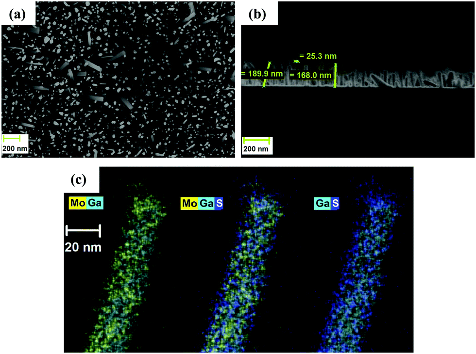 | ||
| Fig. 1 SEM images of GaN NRs on Si showing the (a) top surface and (b) cross-sectional view. (c) Cross-sectional TEM-EDS micrographs of MoS2/GaN NRs, indicating conformal growth of MoS2 around the GaN NRs. | ||
For the performance evaluation of the MoS2/GaN NRs/Si-based PD, spectral response studies were conducted in the wavelength range of 300–1000 nm (0.075 mW cm−2) under self-powered conditions and the results are shown in Fig. 2(a). The response is observed in the entire wavelength range, and the maximum response is obtained at 900 nm. Responsivity starts to increase from the UV region to the visible region, and becomes maximum in the NIR region. Due to the non-uniform and thin coating of MoS2 on GaN NRs as well as Si, a considerable amount of UV and visible light is absorbed by GaN and Si. Hence, a significant photoresponse is obtained in the UV-visible region, in contrast to the PD based on a thicker MoS2 film on GaN thin film/Si as demonstrated in our previous report.23 In the NIR region, the response becomes maximum around 900 nm as the absorbed photons lead to band-to-band transitions in MoS2 and Si, following which the photon energy becomes insufficient to excite the electrons present in the valence band of MoS2 and Si. Thus, the responsivity follows the behavior as observed in Fig. 2(a). I–V characteristics in the dark and under light illumination (λ = 900 nm) are presented in Fig. 2(b). The maximum photocurrent is seen at zero bias (inset of Fig. 2(b)), which shows the self-powered behavior of the PD. The variation in the photocurrent with light intensity was studied and the log(photocurrent) vs. log(power density) plot is shown in Fig. 2(c). Linear fitting of the curve shows a nonlinear dependence of photocurrent on the power density of the incident light (Iph ∝ Pθ, θ = 0.25). This non-unity value of θ suggests that complex processes are involved in the generation of charge carriers i.e., trapping and recombination.34,35Fig. 2(d) depicts the variation of the responsivity and detectivity with illumination power density. Responsivity decreases with an increase in the power density of the incident light source, which can be related to the enhanced recombination or scattering rate of photogenerated charge carriers, because their concentration increases at higher power densities. Just like responsivity, detectivity follows a similar trend and decreases with increasing power density, as the two quantities are directly proportional to each other, and the dark current is the same for different incident power densities. The variation of sensitivity and gain with incident power density is shown in Fig. S4 (ESI†). The temporal response of the device is measured at 0 V (Fig. 3(a)) and a reproducible and stable photoresponse is observed. From the I–t plot, the time interval between the two sampling points comes out to be ∼100 ms, which is limited by the experimental setup. Hence, to estimate the rise and fall time constants with precision and accuracy, an ultrafast time measurement setup has been used (Fig. 3(b)), and the details of this setup have been described elsewhere.33Fig. 3(c–e) depict the transient response of the detector at different chopper frequencies (1, 5 and 10 kHz), and the response/recovery times of the device were estimated by fitting a single response–recovery cycle with given first-order exponential equations. The estimated response/recovery times are as follows: 1 kHz – 164.9/93.8 μs, 5 kHz – 57.2/16.9 μs, and 10 kHz – 38.8/8.2 μs.
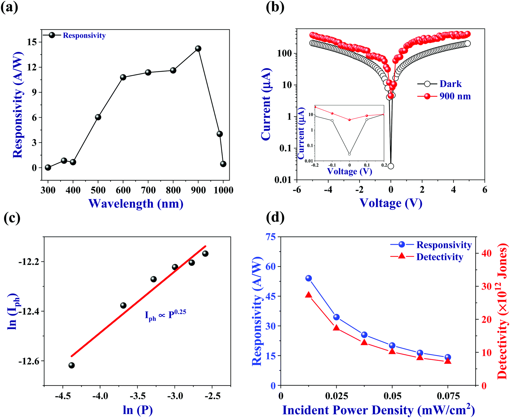 | ||
| Fig. 2 (a) Spectral response, (b) dark and illuminated I–V characteristics of the device (the inset shows a zoomed view of the I–V characteristics near zero bias), (c) variation in photocurrent with different power intensities of irradiated light, and (d) variation in responsivity and detectivity with different power densities of irradiated light for the MoS2/GaN NRs/Si-based device. | ||
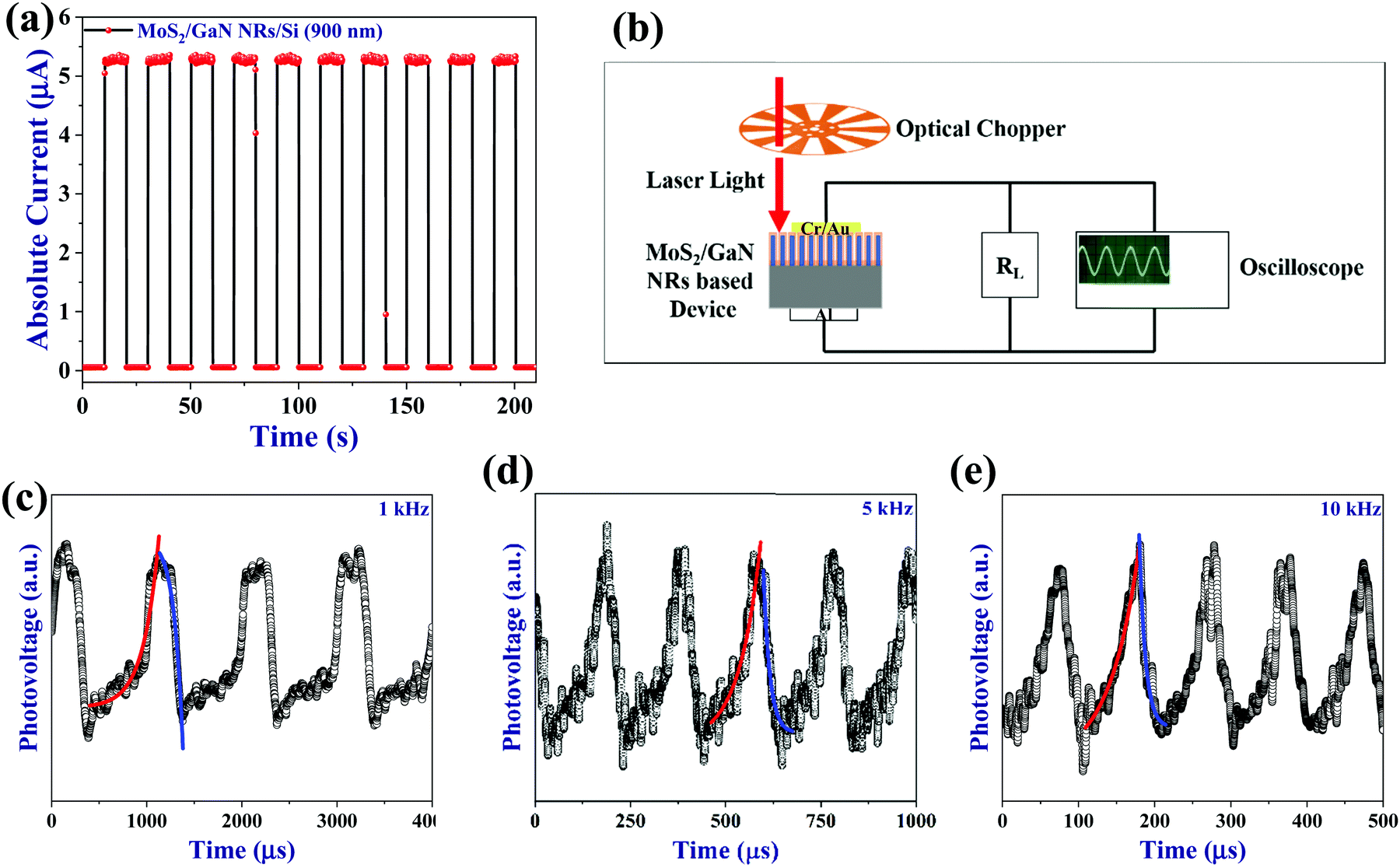 | ||
| Fig. 3 (a) Temporal response of the MoS2/GaN NRs/Si device at 0 V under 900 nm light illumination, (b) schematic of the ultrafast time measurement setup. Temporal response of the MoS2/GaN NRs/Si device at a frequency of (c) 1 kHz, (d) 5 kHz and (e) 10 kHz measured with the ultrafast measurement setup. | ||
It is seen that the response time of the PD is slower than the recovery time. As observed from the power law, the response of a semiconductor to incident photons is a complex process. Therefore, during the photogeneration of carriers, traps and surface states might be playing a significant role, leading to a slower response. In contrast, when the illumination is switched off, a fast charge carrier recombination leads to a quick recovery. A similar trend has been seen in previously reported NR-based PDs.36
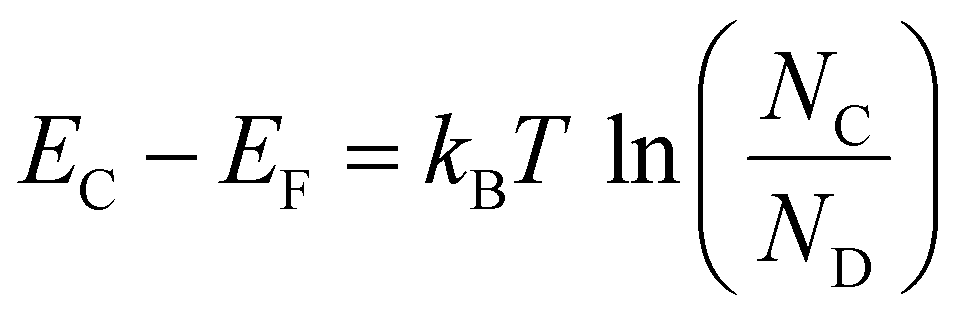
The probable working mechanism of the MoS2/GaN NRs/Si-based PD is explained with the help of the energy band diagrams of the heterojunction. The band gaps of MoS2 and Si have been taken to be ∼1.34 and ∼1.11 eV, respectively, from our previous reports.10,33 The band gap of GaN has been estimated from diffuse reflectance spectroscopy, and is found to be ∼3.37 eV (Fig. S5 of the ESI†). In this case, two different heterojunctions, MoS2/GaN/Si and MoS2/Si, come into the picture as MoS2 is also directly deposited on Si. Using Hall measurements for MoS2/Si and the Si substrate, the carrier concentrations (ND) of MoS2 and Si have been estimated to be ∼4.3 × 10¹⁶ and ∼3.1 × 1012 cm−3, respectively. For estimating the carrier concentration of GaN, we have taken a GaN thin film sample and the carrier concentration is observed to be ∼1.8 × 1019 cm−3. All three samples (MoS2, GaN and Si) show unintentional n-type behavior, and the values of EC − EF are calculated for all three semiconductors using eqn (1):37
 | (1) |
 | (2) |
 | (3) |
 ) of eqn (2) corresponds to the difference in the energy of the Mo core level with respect to its valence band maximum (VBM) and is found to be 228.44 eV (Fig. 4(a)). The subsequent term
 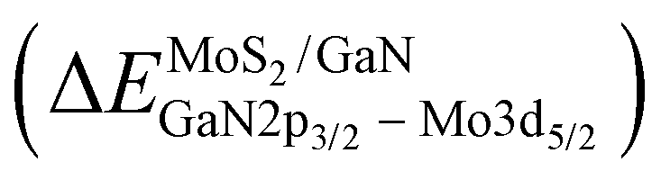 of eqn (2) refers to the energy difference of the Ga and Mo core levels, and is estimated to be 888.60 eV (Fig. 4(b)). The last term (
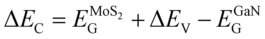
 ) of eqn (2) denotes the energy of the core level of Ga relative to its respective VBM, which is observed to be 1114.88 eV (Fig. 4(c)). Hence, from eqn (2), ΔEV is calculated to be 2.16 eV. In eqn (3), EGaNG and
 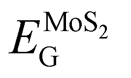 represent the band gaps of GaN and MoS2, respectively. Thus, from eqn (3), ΔEC is found to be 0.28 eV.
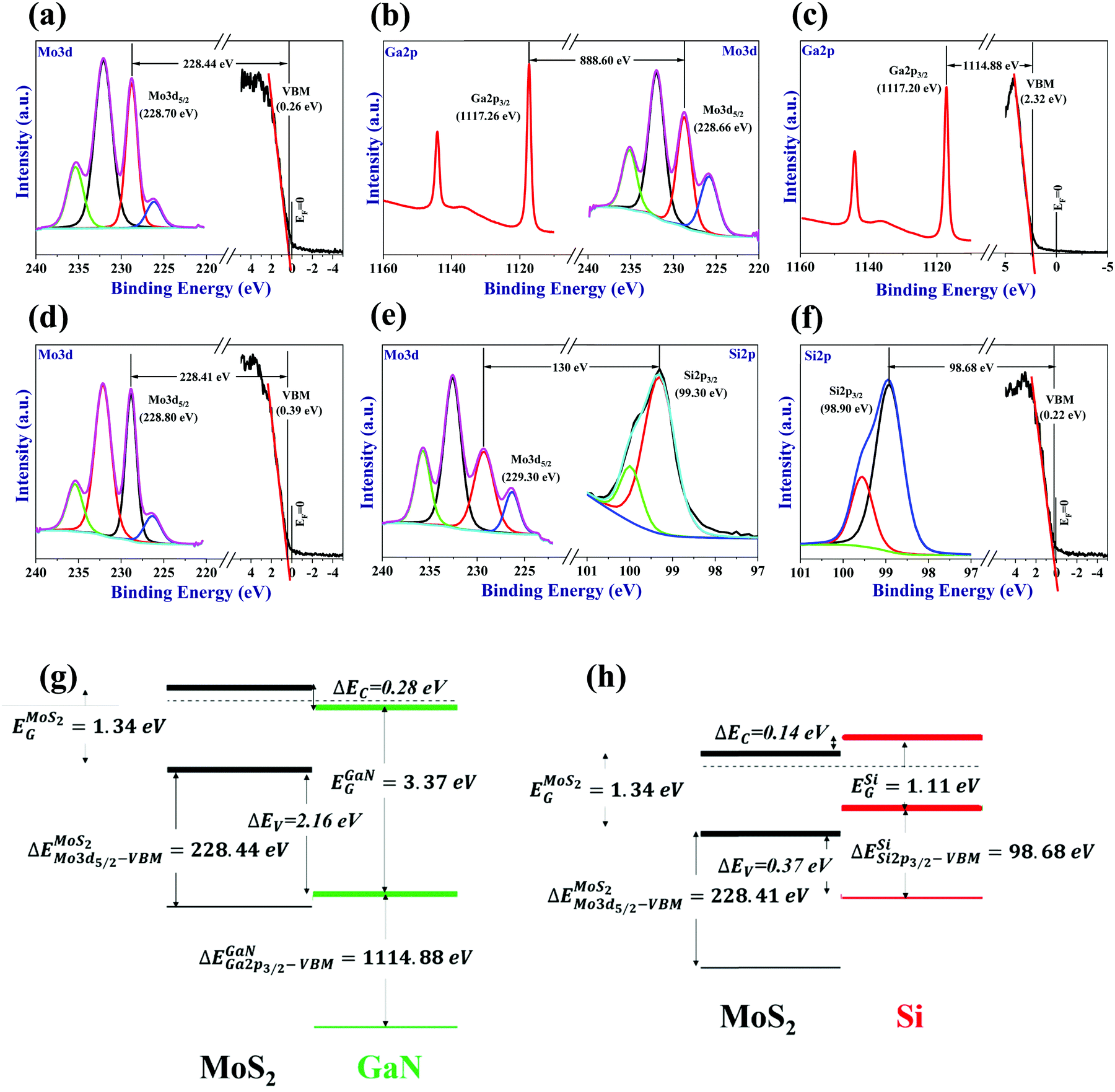 | ||
| Fig. 4 For MoS2/GaN, (a) Mo3d core level and valence band spectra (VBS) acquired from MoS2, (b) Ga2p and Mo3d core-level spectra of the MoS2/GaN heterojunction, and (c) Ga2p core level and VBS of the GaN epilayer. For MoS2/Si, (d) Mo3d core level and VBS acquired from MoS2, (e) Mo3d and Si2p core-level spectra of the MoS2/Si heterojunction, and (f) Si2p core level and VBS of the Si substrate. Band alignment at (g) MoS2/GaN and (h) MoS2/Si heterojunctions. | ||
Similarly, the band offset parameters of MoS2/Si have been determined by substituting the appropriate terms in eqn (2) and (3) with the corresponding values, as shown in Fig. 4(d–f). The VBO and CBO values for the MoS2/Si heterojunction are observed to be −0.37 and −0.14 eV, respectively. Here, the negative sign indicates that the band edges of MoS2 are below those of Si. Based on these band offset values as well as the values of EC − EF obtained from eqn (1), the band alignments at the MoS2/GaN and MoS2/Si heterointerfaces are shown in Fig. 4(g and h). The corresponding energy band diagrams of the MoS2/GaN/Si and MoS2/Si heterojunctions are shown in Fig. S6 (ESI†) and are in agreement with the band alignments evaluated through HRXPS measurements.
When the device is illuminated, electrons and holes are generated at both the MoS2 as well as the Si side. Due to the overall built-in potential developed in the MoS2/GaN NRs/Si heterojunction, electrons in the Si side move into the conduction band of MoS2. Moreover, these electrons are then collected by the electrode at the MoS2 side, whereas the holes remain in the valence bands of MoS2 and Si as depicted in Fig. 5(a). On the other hand, for the MoS2/Si heterojunction, the built-in potential is directed from the MoS2 towards the Si side. Thus, the electrons present in the conduction band of MoS2 and Si are collected by the electrode at the MoS2 side, whereas the photogenerated holes move towards the Si side and are collected by the metal contact on Si because of the built-in potential as shown in Fig. 5(b). In addition, the remnant photogenerated holes in the valence bands of MoS2 and Si in the MoS2/GaN/Si heterojunction move into the valence band of Si (as MoS2 is continuously distributed all over GaN NRs and Si) and are collected by the electrode at the Si side.
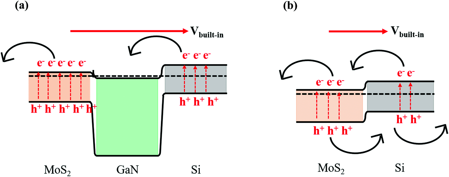 | ||
| Fig. 5 Carrier transport in the self-powered mode for (a) MoS2/GaN NRs/Si and (b) MoS2/Si heterojunctions depicted by energy band diagrams. | ||
Responsivity, detectivity, gain and sensitivity are some important figures of merit used to assess the performance of a detector. We have calculated these figures of merit for a light illumination intensity of 0.075 mW cm−2 at 0 V (λ = 900 nm). The responsivity (Rλ) is the ratio of the photocurrent generated to the incident power density and is calculated by using the following equation:39
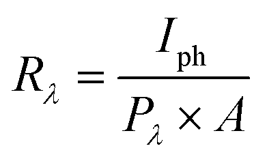 | (4) |
The specific detectivity (D*) can be determined by the relation:39
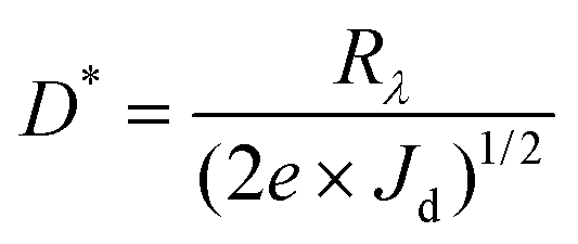 | (5) |
Sensitivity (S) is the ratio of the photocurrent to the dark current of the PD. It is determined using the following equation:39
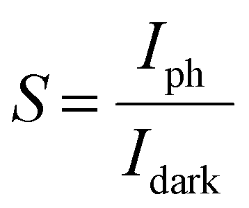 | (6) |
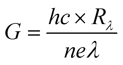
The gain (G) of a PD,39 which can be defined as the number of photogenerated electrons detected per incident photon, assuming that the external quantum efficiency (η) is 100%, is calculated using the following equation:
 | (7) |
From these results, the responsivity, detectivity, sensitivity and gain are estimated to be 14.22 A W−1, 2.72 × 10¹³ Jones, ∼1.17 × 10², and 74.49, respectively, in the self-biased mode (light intensity = 0.075 mW cm−2). The gain achieved for the device is greater than unity, and this can be ascribed to the strong built-in potential present at the interface, which results in effective carrier separation and hole trapping due to the adsorption/desorption of oxygen species. Due to the sulfur vacancies in MoS2, atmospheric oxygen gets adsorbed, capturing the free electrons. When the junction is illuminated with light, electron–hole pairs are created and the photogenerated holes discharge the negatively charged oxygen ions from MoS2. Overall, the adsorption and desorption of the oxygen species on the MoS2 surface play a crucial role in the trapping of holes and prolong the mean lifetime of the holes. When the mean lifetime of the holes becomes larger than the transit time of the electrons, a high internal gain can be achieved.33,40,41 To reveal the influence and the importance of MoS2, spectral response measurements of the MoS2/GaN NRs/Si-based device (in the top–top contact configuration, i.e. by taking both the contacts from the top) as well as the GaN NRs/Si-based device have been carried out in the self-powered mode for comparison. It has been observed that the maximum responsivity in the case of the top–top contact configuration is ∼1.83 A W−1 (at a wavelength of 986 nm), whereas, for the case of the GaN NRs/Si-based PD, the maximum responsivity is found to be ∼150 mA W−1 (at a 364 nm wavelength). Moreover, the response in this case is higher in the UV region as compared to that in the visible/NIR region due to the absence of MoS2. These results are presented in Fig. S7 of the ESI.†
The performance parameters of our device are summarized in Table 1 and compared with those of several reported PDs from the literature (working wavelength in the NIR region). It can be clearly deduced from this comparison that our hybrid NRs-based device shows excellent performance exhibiting a self-biased, broadband and ultrafast photoresponse. These results show that devices based on the 1D–2D conformal architecture can be a route towards the advancement of futuristic electronics. We have also compared our MoS2/GaN NRs/Si-based PD with a previously reported MoS2/GaN film/Si-based device.23 It may be noted that the device shows a broadband photoresponse along with a much-pronounced response in the visible region as GaN NRs also contribute to the photocurrent, in contrast to the narrow range detection obtained in the case of the GaN film-based PD.23 Furthermore, the response is maximum at 900 nm instead of 995 nm.23 We believe the differences are due to the very low thickness of MoS2 on GaN NRs. Moreover, due to the lower channel width in the case of GaN NRs, the response/recovery is much faster as compared to the GaN film-based device. In addition, the phenomenon of polarity inversion is missing in the present case, and the most plausible reason for this could be the low thickness as well as the non-uniform distribution of MoS2 over GaN NRs, which may result in the development of thermoelectric potential which is insufficient to separate electrons and holes. Furthermore, the difference in the observed photodetection behavior may also be due to the different growth orientations of GaN in the case of MoS2/GaN film/Si and MoS2/GaN NRs/Si-based PDs. Thus, a thorough study is required for better understanding of these different behaviors.
| Photodetector | Bias (V) | Responsivity (mA W−1) | Detectivity (Jones) | Rise/fall time (ms) |
|---|---|---|---|---|
| MoS2/GaN42 | 20 | ∼5 × 10⁻¹ @ 900 nm | − | −/− |
| GeSe43 | 2 | 63 @ 900 nm (1.5 W m−2) | 8 × 10⁸ | − |
| PbS quantum dots/graphene44 | 4 | 6.81 × 10³ @ 900 nm (27.5 μW) | − | 300/3.2 × 103 |
| MoTe2/monolayer graphene45 | V D = 1 | 9.71 × 10⁵ @ 1064 nm (202 μW) | 1.55 × 10¹¹ | 78/375 |
| MoTe246 | V D = 10, VG = 10 | 24 @ 1060 nm (20 nW) | 1.30 × 10⁹ | 1.6/1.3 |
| Black phosphorus47 | V D = −1, VG = −15 | ∼1 × 10⁶ @ 900 nm (5 mW cm−2) | − | ∼5/− |
| WSe2/SnSe248 | V D = −3, VG = −100 | 3.96 × 10⁵ @ 980 nm (100 mW cm−2) | 4.40 × 10¹⁰ | 16/45 |
| MoS2/Si49 | 0 | 300 @ 808 nm (10 mW cm−2) | ∼1013 | 0.003/0.040 |
| MoS2/GaN50 | 1 | 8 × 10⁴ @ 850 nm (2 mW cm−2) | − | ∼2.4 × 10³/∼9 × 103 |
| MoS2/GaN NRs/Si (this work) | 0 | 1.42 × 10⁴ @ 900 nm (0.075 mW cm−2) | 2.72 × 10¹³ | 0.039/0.008 |
4 Conclusions
In conclusion, we have reported the conformal growth of MoS2 on GaN NRs and a broadband, self-biased and ultrafast PD based on the MoS2/GaN NRs/Si heterostructure is demonstrated. The PD shows a high photoresponsivity of 14.22 A W−1 in the self-powered mode for low intensity light illumination along with an ultrafast photoresponse with a rise/fall time of 38.8/8.2 μs. We believe that this study could provide a very important step towards engineering core–shell nanostructured devices in the field of low power optoelectronics.Conflicts of interest
The authors declare no conflicts of interest.Acknowledgements
The authors thank Dr. Arun Malla Chowdhury, Dr. Basanta Roul and Ms. Malti Kumari for useful discussions and help in characterization. The authors acknowledge Prof. Kausik Majumdar and Mr Nithin Abraham from the Department of Electrical Communication Engineering, Indian Institute of Science, Bangalore, India for their assistance in ultrafast time measurements. The authors are thankful to Mr. Ambresh M. for his help in TEM and its sample preparation. The authors also thank Mr. Debashis Tripathy from the Department of Inorganic and Physical Chemistry, Indian Institute of Science, Bangalore, India for assistance in HRXPS measurements. D. K. S. is thankful to the Council of Scientific and Industrial Research (CSIR), Government of India, New Delhi and Indian Institute of Science, Bangalore, India for providing a senior research fellowship and research associateship, respectively. S. B. K. acknowledges the INSA senior scientist fellowship.References
- S. M. Hatch, J. Briscoe and S. Dunn, A Self-Powered ZnO-Nanorod/CuSCN UV Photodetector Exhibiting Rapid Response, Adv. Mater., 2013, 25(6), 867–871 CrossRef CAS PubMed.
- D. K. Singh, K. K. Nanda and S. B. Krupanidhi, Pulsed Laser Deposition of Transition Metal Dichalcogenides-Based Heterostructures for Efficient Photodetection, in Practical Applications of Laser Ablation, ed. D. Yang, IntechOpen, 2021 DOI:10.5772/intechopen.94236.
- R. Pant, D. K. Singh, A. M. Chowdhury, B. Roul, K. K. Nanda and S. B. Krupanidhi, Next-Generation Self-Powered and Ultrafast Photodetectors Based on III-Nitride Hybrid Structures, APL Mater., 2020, 8(2), 020907 CrossRef CAS.
- W. Wu, Q. Zhang, X. Zhou, L. Li, J. Su, F. Wang and T. Zhai, Self-Powered Photovoltaic Photodetector Established on Lateral Monolayer MoS2-WS2 Heterostructures, Nano Energy, 2018, 51, 45–53 CrossRef CAS.
- R. K. Singh, J. Kumar, A. Kumar, V. Kumar, R. Kant and R. Singh, Poly(3-Hexylthiophene): Functionalized Single-Walled Carbon Nanotubes: (6,6)-Phenyl-C61-Butyric Acid Methyl Ester Composites for Photovoltaic Cell at Ambient Condition, Sol. Energy Mater. Sol. Cells, 2010, 94(12), 2386–2394 CrossRef CAS.
- K. L. Kumawat, D. K. Singh, K. K. Nanda and S. B. Krupanidhi, Solution-Processed SnSe2-RGO based Bulk Heterojunction for Self-Powered and Broadband Photodetection, ACS Appl. Electron. Mater., 2021, 3(7), 3131–3138 CrossRef CAS.
- U. Varshney, N. Aggarwal and G. Gupta, Current Advances in Solar-Blind Photodetection Technology: Using Ga2O3 and AlGaN, J. Mater. Chem. C, 2022, 10(5), 1573–1593 RSC.
- R. Wadhwa, A. V. Agrawal, D. Kushavah, A. Mushtaq, S. K. Pal and M. Kumar, Investigation of charge transport and band alignment of MoS2-ReS2 heterointerface for high performance and self-driven broadband photodetection, Appl. Surf. Sci., 2021, 569, 150949 CrossRef CAS.
- R. Zhuo, Y. Wang, D. Wu, Z. Lou, Z. Shi, T. Xu, J. Xu, Y. Tian and X. Li, High-Performance Self-Powered Deep Ultraviolet Photodetector Based on MoS2/GaN p–n Heterojunction, J. Mater. Chem. C, 2018, 6(2), 299–303 RSC.
- D. K. Singh, B. Roul, R. Pant, A. M. Chowdhury, K. K. Nanda and S. B. Krupanidhi, Different Types of Band Alignment at MoS2/(Al, Ga, In)N Heterointerfaces, Appl. Phys. Lett., 2020, 116(25), 252102 CrossRef CAS.
- G. Konstantatos, Current Status and Technological Prospect of Photodetectors Based on Two-Dimensional Materials, Nat. Commun., 2018, 9(1), 5266 CrossRef CAS PubMed.
- N. Huo, Y. Yang, Y.-N. Wu, X.-G. Zhang, S. T. Pantelides and G. Konstantatos, High Carrier Mobility in Monolayer CVD-Grown MoS2 through Phonon Suppression, Nanoscale, 2018, 10(31), 15071–15077 RSC.
- N. Huo and G. Konstantatos, Ultrasensitive All-2D MoS2 Phototransistors Enabled by an out-of-Plane MoS2 PN Homojunction, Nat. Commun., 2017, 8(1), 572 CrossRef PubMed.
- M.-H. Chiu, W.-H. Tseng, H.-L. Tang, Y.-H. Chang, C.-H. Chen, W.-T. Hsu, W.-H. Chang, C.-I. Wu and L.-J. Li, Band Alignment of 2D Transition Metal Dichalcogenide Heterojunctions, Adv. Funct. Mater., 2017, 27(19), 1603756 CrossRef.
- N. Li, Z. Wei, J. Zhao, Q. Wang, C. Shen, S. Wang, J. Tang, R. Yang, D. Shi and G. Zhang, Atomic Layer Deposition of Al2O3 Directly on 2D Materials for High-Performance Electronics, Adv. Mater. Interfaces, 2019, 6(10), 1802055 CrossRef.
- M. Long, P. Wang, H. Fang and W. Hu, Progress, Challenges, and Opportunities for 2D Material Based Photodetectors, Adv. Funct. Mater., 2019, 29(19), 1803807 CrossRef.
- F. Gao, H. Yang and P. Hu, Interfacial Engineering for Fabricating High-Performance Field-Effect Transistors Based on 2D Materials, Small Methods, 2018, 2(6), 1700384 CrossRef.
- D. K. Singh, Layered Metal Dichalcogenides-Based Hybrid Devices for Resistive Sensing, Indian Institute of Science, India, 2021 Search PubMed.
- M. Meneghini, G. Meneghesso and E. Zanoni, Power GaN Devices: Materials, Applications and Reliability, Power Electronics and Power Systems, Springer International Publishing, Cham, 2017 DOI:10.1007/978-3-319-43199-4.
- C.-Y. Huang, C. Chang, G.-Z. Lu, W.-C. Huang, C.-S. Huang, M.-L. Chen, T.-N. Lin, J.-L. Shen and T.-Y. Lin, Hybrid 2D/3D MoS2/GaN Heterostructures for Dual Functional Photoresponse, Appl. Phys. Lett., 2018, 112(23), 233106 CrossRef.
- S. K. Jain, R. R. Kumar, N. Aggarwal, P. Vashishtha, L. Goswami, S. Kuriakose, A. Pandey, M. Bhaskaran, S. Walia and G. Gupta, Current Transport and Band Alignment Study of MoS2/GaN and MoS2/AlGaN Heterointerfaces for Broadband Photodetection Application, ACS Appl. Electron. Mater., 2020, 2(3), 710–718 CrossRef CAS.
- X. Zhang, J. Li, Z. Ma, J. Zhang, B. Leng and B. Liu, Design and Integration of a Layered MoS2/GaN van der Waals Heterostructure for Wide Spectral Detection and Enhanced Photoresponse, ACS Appl. Mater. Interfaces, 2020, 12(42), 47721–47728 CrossRef CAS PubMed.
- D. K. Singh, R. K. Pant, K. K. Nanda and S. B. Krupanidhi, Differentiation of Ultraviolet/Visible Photons from near Infrared Photons by MoS2/GaN/Si-Based Photodetector, Appl. Phys. Lett., 2021, 119(12), 121102 CrossRef CAS.
- L. Goswami, N. Aggarwal, M. Singh, R. Verma, P. Vashishtha, S. K. Jain, J. Tawale, R. Pandey and G. Gupta, GaN Nanotowers Grown on Si(111) and Functionalized with Au Nanoparticles and ZnO Nanorods for Highly Responsive UV Photodetectors, ACS Appl. Nano Mater., 2020, 3(8), 8104–8116 CrossRef CAS.
- M. S. Son, S. I. Im, Y. S. Park, C. M. Park, T. W. Kang and K.-H. Yoo, Ultraviolet Photodetector Based on Single GaN Nanorod p–n Junctions, Mater. Sci. Eng., C, 2006, 26(5–7), 886–888 CrossRef CAS.
- M. Reddeppa, S. B. Mitta, T. Chandrakalavathi, B.-G. Park, G. Murali, R. Jeyalakshmi, S.-G. Kim, S. H. Park and M.-D. Kim, Solution-Processed Au@rGO/GaN Nanorods Hybrid-Structure for Self-Powered UV, Visible Photodetector and CO Gas Sensors, Curr. Appl. Phys., 2019, 19(8), 938–945 CrossRef.
- G. Yang, Y. Gu, P. Yan, J. Wang, J. Xue, X. Zhang, N. Lu and G. Chen, Chemical Vapor Deposition Growth of Vertical MoS2 Nanosheets on p-GaN Nanorods for Photodetector Application, ACS Appl. Mater. Interfaces, 2019, 11, 8453–8460 CrossRef CAS PubMed.
- A. V. Agrawal, K. Kaur and M. Kumar, Interfacial Study of Vertically Aligned N-Type MoS2 Flakes Heterojunction with p-Type Cu–Zn–Sn–S for Self-Powered, Fast and High Performance Broadband Photodetector, Appl. Surf. Sci., 2020, 514, 145901 CrossRef CAS.
- B. Cai, Y. Zhao, Z. Zhang and G. Ouyang, Interfacial Charge Transfer and Photovoltaic Properties in C60/MoS 2 0D–2D van der Waals Heterostructures, Phys. Status Solidi RRL, 2021, 15(10), 2100311 CrossRef CAS.
- D. Jariwala, T. J. Marks and M. C. Hersam, Mixed-Dimensional van der Waals Heterostructures, Nat. Mater., 2017, 16(2), 170–181 CrossRef CAS PubMed.
- Y. Liu, Y. Huang and X. Duan, van der Waals Integration before and beyond Two-Dimensional Materials, Nature, 2019, 567(7748), 323–333 CrossRef CAS PubMed.
- B. Roul, R. Pant, S. Chirakkara, G. Chandan, K. K. Nanda and S. B. Krupanidhi, Enhanced UV Photodetector Response of ZnO/Si With AlN Buffer Layer, IEEE Trans. Electron Devices, 2017, 64(10), 4161–4166 CAS.
- D. K. Singh, R. Pant, A. M. Chowdhury, B. Roul, K. K. Nanda and S. B. Krupanidhi, Defect-Mediated Transport in Self-Powered, Broadband, and Ultrafast Photoresponse of a MoS2/AlN/Si-Based Photodetector, ACS Appl. Electron. Mater., 2020, 2(4), 944–953 CrossRef CAS.
- D. K. Singh, R. Pant, B. Roul, A. M. Chowdhury, K. K. Nanda and S. B. Krupanidhi, Temperature-Dependent Electrical Transport and Optoelectronic Properties of SnS2/p-Si Heterojunction, ACS Appl. Electron. Mater., 2020, 2(7), 2155–2163 CrossRef CAS.
- Q. Zhao, W. Wang, F. Carrascoso-Plana, W. Jie, T. Wang, A. Castellanos-Gomez and R. Frisenda, The Role of Traps in the Photocurrent Generation Mechanism in Thin InSe Photodetectors, Mater. Horiz., 2020, 7(1), 252–262 RSC.
- P. Feng, J. Y. Zhang, Q. H. Li and T. H. Wang, Individual β-Ga2O3 Nanowires as Solar-Blind Photodetectors, Appl. Phys. Lett., 2006, 88(15), 153107 CrossRef.
- B. Roul, R. Pant, A. M. Chowdhury, G. Chandan, D. K. Singh, S. Chirakkara, K. K. Nanda and S. B. Krupanidhi, Highly Responsive ZnO/AlN/Si Heterostructure-Based Infrared- and Visible-Blind Ultraviolet Photodetectors With High Rejection Ratio, IEEE Trans. Electron Devices, 2019, 66(3), 1345–1352 CAS.
- E. A. Kraut, R. W. Grant, J. R. Waldrop and S. P. Kowalczyk, Precise Determination of the Valence-Band Edge in X Ray Photoemission Spectra, Phys. Rev. Lett., 1980, 44(24), 1620–1623 CrossRef CAS.
- D. K. Singh, B. Roul, K. K. Nanda and S. B. Krupanidhi, Group III-Nitrides and Their Hybrid Structures for Next-Generation Photodetectors, in Light-Emitting Diodes and Photodetectors - Advances and Future Directions, ed. M. Casalino, IntechOpen, 2021 DOI:10.5772/intechopen.95389.
- W. Jin, Y. Ye, L. Gan, B. Yu, P. Wu, Y. Dai, H. Meng, X. Guo and L. Dai, Self-Powered High Performance Photodetectors Based on CdSe Nanobelt/Graphene Schottky Junctions, J. Mater. Chem., 2012, 22(7), 2863 RSC.
- J. Wang, Y. Chang, L. Huang, K. Jin and W. Tian, Designing CdS/Se Heterojunction as High-Performance Self-Powered UV-Visible Broadband Photodetector, APL Mater., 2018, 6(7), 076106 CrossRef.
- S. V. Solanke, S. Rathkanthiwar, A. Kalra, R. K. Mech, M. Rangarajan, S. Raghavan and D. N. Nath, Integration of multi-layered materials with wide bandgap semiconductors for multi-spectral photodetectors: Case for MoS2/GaN and β-In2Se3/GaN, Semicond. Sci. Technol., 2019, 34(7), 075020 CrossRef CAS.
- Z. Wang, M. Li, X. P. Gao and Z. Zhang, Broadband photodetection of GeSe films of vertically grown nanoflakes, ACS Appl. Electron. Mater., 2019, 1(11), 2236–2243 CrossRef CAS.
- B. Cook, M. Gong, D. Ewing, M. Casper, A. Stramel, A. Elliot and J. Wu, Inkjet Printing Multicolor Pixelated Quantum Dots on Graphene for Broadband Photodetection, ACS Appl. Nano Mater., 2019, 2(5), 3246–3252 CrossRef CAS.
- W. Yu, S. Li, Y. Zhang, W. Ma, T. Sun, J. Yuan, K. Fu and Q. Bao, Near-infrared photodetectors based on MoTe2/graphene heterostructure with high responsivity and flexibility, Small, 2017, 13(24), 1700268 CrossRef PubMed.
- H. Huang, J. Wang, W. Hu, L. Liao, P. Wang, X. Wang, F. Gong, Y. Chen, G. Wu, W. Luo and H. Shen, Highly sensitive visible to infrared MoTe2 photodetectors enhanced by the photogating effect, Nanotechnology, 2016, 27(44), 445201 CrossRef PubMed.
- M. Huang, M. Wang, C. Chen, Z. Ma, X. Li, J. Han and Y. Wu, Broadband black-phosphorus photodetectors with high responsivity, Adv. Mater., 2016, 28(18), 3481–3485 CrossRef CAS PubMed.
- H. Xue, Y. Dai, W. Kim, Y. Wang, X. Bai, M. Qi, K. Halonen, H. Lipsanen and Z. Sun, High photoresponsivity and broadband photodetection with a band-engineered WSe2/SnSe2 heterostructure, Nanoscale, 2019, 11(7), 3240–3247 RSC.
- L. Wang, J. Jie, Z. Shao, Q. Zhang, X. Zhang, Y. Wang, Z. Sun and S. T. Lee, MoS2/Si heterojunction with vertically standing layered structure for ultrafast, high-detectivity, self-driven visible–near infrared photodetectors, Adv. Funct. Mater., 2015, 25(19), 2910–2919 CrossRef CAS.
- S. K. Jain, M. X. Low, P. D. Taylor, S. A. Tawfik, M. J. S. Spencer, S. Kuriakose, A. Arash, C. Xu, S. Sriram, G. Gupta, M. Bhaskaran and S. Walia, 2D/3D Hybrid of MoS2/GaN for a High-Performance Broadband Photodetector, ACS Appl. Electron. Mater., 2021, 3(5), 2407–2414 CrossRef CAS.
Footnote |
| † Electronic supplementary information (ESI) available: Schematic of the device, Raman spectra and glancing angle XRD of MoS2, morphology of MoS2/GaN NRs, variation of sensitivity and gain with power density of the incident light for the MoS2/GaN NRs/Si based device, band gap estimation of GaN, energy band diagrams of MoS2/GaN/Si and MoS2/Si heterojunctions, responsivity as a function of wavelength for the MoS2/GaN NRs/Si-based device in two different configurations: top–top contact and top–bottom contact, along with a comparison with the GaN NRs/Si-based device. See DOI: https://doi.org/10.1039/d2ma00577h |
| This journal is © The Royal Society of Chemistry 2022 |