
 Open Access Article
 This Open Access Article is licensed under a Creative Commons Attribution-Non Commercial 3.0 Unported Licence
Memristive perovskite solar cells towards parallel solar energy harvesting and processing-in-memory computing†
Konstantinos
Rogdakis
 *ab,
Michalis
Loizos
a,
George
Viskadouros
a and
Emmanuel
Kymakis
*ab
*ab,
Michalis
Loizos
a,
George
Viskadouros
a and
Emmanuel
Kymakis
*ab
aDepartment of Electrical & Computer Engineering, Hellenic Mediterranean University (HMU), Heraklion 71410, Crete, Greece. E-mail: krogdakis@hmu.gr; kymakis@hmu.gr
bInstitute of Emerging Technologies (i-EMERGE) of HMU Research Center, Heraklion 71410, Crete, Greece
First published on 11th July 2022
Abstract
The heterogeneity of peculiar ions and carriers observed in hybrid organic/inorganic materials is the source of their emergent cross-coupled light and electric field tuneable functions with potential utility in novel opto-electronic applications. Notably, mixed halide perovskites (HPs) have been used as active layers in high performing perovskite solar cells (PSCs) that led to efficient solar energy harvesting. Their rich dynamics enabled by inherently coupled ionic and electronic degrees of freedom have also led to the demonstration of optoelectronic memristors that emulate synaptic- and neural-like dynamics. Consequently, a printable single material stack fabricated at low temperature combining both solar energy harvesting and memristive functionalities attainable at low switching voltages would constitute a transformational breakthrough. In this study, we have demonstrated an inverted PSC with an average power conversion efficiency (PCE) of ∼17% that with appropriate electric biasing procedure exhibits stable resistance switching characteristics at low voltages without losing its PCE performance even after thousands of switching cycles (hereafter this device is termed as MemPVCell). In particular, the MemPVCell demonstrates a high resistance state (HRS) to low resistance state (LRS) ratio of up to 105 and light-tunable switching cycles in the millisecond regime with an endurance of 3 × 10³ cycles with no detectable HRS/LRS ratio drop. During state retention tests, the HRS exhibits no change in time, while the LRS gradually increases resulting in an overall HRS/LRS ratio retention of up to 3600 s with less than a 30% drop of its initial value in the optimum device configuration. Corresponding PCE performance was monitored after using multiple dc resistance switching loops and pulsed endurance cycles, demonstrating full PCE recovery to its initial value within a few minutes of rest. Complementary transient electrochemical impedance spectroscopy (EIS) measurements supported the MemPVCell switching effects. Aiming at further improving the device performance, modifications of MemPVCell's layered structure were investigated, a process that allowed identification of each layer's impact on the parallel photovoltaic and memristive switching characteristics. As a proof of concept towards neuromorphic circuits, basic synaptic functionalities tunable by light are demonstrated such as potentiation and depreciation protocols, short-term plasticity (STP) and long-term plasticity (LTP) effects and associated spike-timing dependent plasticity (STDP).
Introduction
Technologies implementing autonomous smart devices into an Internet-of-Things (IoT) network are increasingly required in our society. A largely distributed network of wireless sensors and wearables is currently connected in the cloud. One of the most challenging bottlenecks in achieving the future vision of the IoT involves powering a multitude of devices, therefore posing critical requirements on their power consumption. These IoT platforms create a robust demand for energy for their power supply, while their ever-increasing number requires ultra-low-power edge-device computing for big data processing.1 The inherent bottlenecks of Si-based CMOS processors due to their energy inefficient von Neumann computation architecture associated with the ‘memory wall’ issue2 lead to unsustainable energy cost in IoT data-centric intensive tasks.3 IoT edge devices4 are usually not capable of data processing and rely on energy-consuming and high-latency cloud communication. Most Si-based IoT devices depend on a battery as their power source, and, therefore, fail to meet the design goals of lifetime power supply, low-cost, reliable sensing, and secure data transmission, demanding radically new material approaches, as well as novel device physics and computing principles.Energy harvesting is a potential alternative to evade recurrent battery replacement, while distinct neuromorphic memristive crossbar arrays are promising solutions for IoT-oriented energy efficient computing,5 pattern recognition and visual pre-processing,6 presenting unique advantages over von Neumann architectures. Several emerging device concepts beyond a von Neumann architecture have led to some successful commercial products, such as Adesto's Moneta electrochemical metallization memory for low-energy applications.7 Two terminal (2T) memristors have attracted great interest as single synaptic units with high scalability, 3D integration capability, and fast switching speed.3,5,6 Large area memristor crossbar arrays have the potential to perform vector-matrix multiplication directly utilizing Ohm's and Kirchhoff's laws, while their inherent properties render them suitable for both digital and analogue computation.3
Memristors’ processing-in-memory can impact numerous application areas upon resolving the sneak path current and half-select issues.3,5 Conventional memristors operating in a linear regime show an output of high current, potentially limiting their power efficiency and scalability.5–7 Alternatively, lower conductance nonlinear memristors, such as those that are ferroelectric based, have the potential for linear computation at ultralow currents towards 100 Gops mW−1.8 Optoelectronic memristors9 have become promising candidates for artificial vision, allowing temporary memory and real-time processing of visual information and sensory data.6 However, challenges such as reliability, device-to-device variation, and large-scale integration exist due to sophisticated fabrication and complex device architectures (rigid, costly), hindering memristive hardware from going mainstream.
The first generation neuromorphic synaptic devices were based on oxide memristors and have demonstrated advantages in terms of scalability, speed, and power consumption. However, “scaling up” toward a practical system size by “scaling down” device dimensions is increasingly challenging.10 New approaches in materials, devices, architecture, and algorithm design are necessary to emulate the scale, functional connectivity, and energy efficiency of biological spiking neural networks.
Hybrid organic/inorganic material-based electronics offer the promise of a mixed ionic/electronic conductivity that has led to systems exhibiting basic functions of neural networks, including synaptic-level functions, such as short- and long-term plasticity (STP and LTP), and system-level properties such as spatiotemporal processing and homeostatic control.11–14 The mechanical properties of organic materials match those of tissues, and the working mechanisms, involving ions, in addition to electrons, are compatible with human physiology.15 Another advantage of organic materials is the potential to introduce novel fabrication techniques relying on additive manufacturing (AM) amenable to one-of-a-kind form factors, making printable organic neuromorphic devices a perfect fit where bioinspiration and bio-integration are required.15
Among the many other types of electronic devices,16–22 perovskite materials were also utilized in memristor devices, initially in their oxide form before the emergence of mixed halide perovskite (HP) materials, due to their ferroelectric properties.23 HPs owing to their intrinsic hysteresis and abundance of charge migration pathways are very promising for memristor applications,24–29 apart from their exceptional power conversion efficiency (PCE) acting as active layers in solar cells.30–33 Since the first report on organic–inorganic HP-based memristors,34 various perovskite compounds have been employed: these include HPs,35 2D organic–inorganic perovskites,36 all-inorganic perovskites,37 and lead-free38 perovskites. Notably, hybrid HPs also intrinsically incorporate richer dynamics in their switching behavior when compared to their inorganic counterparts. Specifically for HPs, apart from the coexistence and coupling of ionic and electronic degrees of freedom, unique is also the light/electrically tunable majority carrier concentrations, opening the path to solar brain realization.1,39 Moreover, hybrid HPs were used in memristive devices that can be programmed to two or more stable conductance states for analogue computing.10
Resistive switching in perovskites is reported to have either an electroforming origin attributed to the formation and rupture of a conductive filament between the bottom and top electrode40,41 or an interface-dominated switching mechanism.42,43 In Table S1 (ESI†), a literature summary of various perovskite-based memristors is shown in comparison with the devices of the present study indicating their high endurance. In the majority of the reported studies, the electrochemically active Ag is used as the top electrode, thus the application of an electric bias results in the migration of Ag cations and the formation of a conducting bridge between the Ag top and the bottom electrode (usually ITO or Pt). The chemical composition of the perovskite active layer was shown to affect the memristive properties of the devices, whereas the mobile Br−, MA+ and I− are reported to be sources of limited endurance and retention characteristics.27,41 In particular, the incorporation of multiple cations such as Rb while suppressing the MA/Rb ratio41 is reported to be beneficial for filament stability resulting in improved endurance and retention characteristics.
Light illumination is shown to have different effects on the memristor current depending on whether the charge transport mechanism is either filament40,41 or interface dominated.42,43 In devices where a filament is formed (mainly originating from iodine vacancies (VI)), light illumination leads to current suppression. This is attributed to a light-assisted ion-vacancy recombination process enabled by photo-induced halide redistribution that leads to filament suppression and thus overall resistance increase upon illumination.44,45 In the case of interface-dominated memristive switching, light exposure leads to an overall current enhancement that is attributed to a photogenerated electric field that lowers interface Schottky barriers driven by trapped photogenerated holes or vacancies.42,43 Table S2 (ESI†) presents a comparison of different memristor technologies in terms of switching characteristics and mechanisms, while in Table S3 (ESI†), a literature overview of various memristive technologies is presented in terms of multifunctionalities offered such as PV, memory, photo-memristor and -synaptic functions.
HP memristor devices can exhibit good properties with ON/OFF ratios ranging from 10 up to 106, but are typically higher than 103. The endurance and retention of these devices can be up to 103–104 cycles and 103–105 s, respectively.46 For instance, Zhou et al. fabricated CH3NH3PbI3−XClX memristors with light-tuneable switching behavior and the ability to perform logic operations. The devices exhibited an ON/OFF ratio of 104, an endurance of 50 cycles and a retention time of 4 × 10⁴ s.
In addition, along with traditional oxide memristors that have shown synaptic and photo-synaptic ability,47,48 both HP and 2D material-based devices have also shown photo-synaptic abilities. In 2016, Xiao et al. reported a MAPbI3-based memristor with applications in neuromorphic computing.49 To compensate for the stability issues, the toxicity and the environmental hazard mitigation of Pb, lead-free devices are also being employed. These low-dimensional layered compounds ensure memristors with low operating voltages and switching yield compared to HP devices, with excellent properties and higher ON/OFF ratios compared to 3D lead-based compounds. The endurance and retention of these devices are in the range of 102–103 cycles and 104–105 s, respectively.50 Gil Kim et al. fabricated memristor devices based on 2D perovskites with an ON/OFF ratio of 108, an endurance and retention of 103 cycles and 104 s, respectively. Furthermore, these devices have shown synaptic behavior.51 The wide variety and range of optoelectronic phenomena these materials portray offer immense potential to multibit memory storage and multimodal accessibility that could be utilized for neuromorphic computing. As an example of 2D material-based memristors, Abnavi et al. reported a MoS2 memristor device and photo-synapses.52 Seo et al. fabricated an h-BN/WSe2 optic-neural synaptic device, demonstrating color-mixed pattern recognition.53
Notably, it was recently demonstrated by M. L. Cantu et al. that additive engineering in HPs can be used to control shallow defects leading to optimized ion mobility and migration, hence establishing a route for efficient and highly stable PSCs.54 A hybrid photovoltaic memristor, namely an organic solar cell with an inverted structure incorporating a ferroelectric transition metal oxide as an electron transport layer (ETL), was demonstrated in the pioneering work of L. Cantu et al., indicating the ability to control the short circuit current (Jsc) by switching the ferroelectric polarization of the ETL.39,55 A similar photovoltaic memristive solar cell with a planar normal structure using a perovskite active layer and a ferroelectric ETL was also reported by the same group.56 Their work opened the path towards a light-tuneable memristor; however, the ferroelectric oxide requires a high temperature for its synthesis – a process incompatible with flexible substrates, – while it also limits the PCE to low values of ∼11% and requires high switching voltages (>15 V).55,56
IoT technologies could benefit from neuromorphic flexible systems based on HPs that could offer massively parallel computing within a more fault-tolerant architecture, opening the path towards reducing the manufacturing cost and power consumption at the IoT edge.5 A fully printable memristive PSC structure could, therefore, exhibit enhanced performance by combining features of both solar cells and memristors in a single stack, enabling light and electrical tunability at low manufacturing temperatures and being compatible with flexible substrates. In this work, we have demonstrated a memristive PSC (termed as MemPVCell) fulfilling the above requirements using a quadruple cation-based perovskite. MemPVCell demonstrates a PCE of ∼17% that upon appropriate memristive channel formation exhibits stable resistance switching characteristics tuneable at low voltages (<1 V) without losing its PCE performance even after thousands of switching cycles. Depending on the MemPVCell layers’ structure, an HRS/LRS ratio of up to 105 was reported with a cycling endurance of >3 × 10³ s with no apparent HRS/LRS ratio drop and extended retention characteristics for the HRS and the LRS (zero and 30% change in the HRS and the LRS, respectively, after 3.6 × 10³ s). Parallel monitoring of the MemPVCell PCE after stress-inducing dc and ac memristive switching measurements revealed a full PCE recovery to its initial value within a few minutes at rest. Lastly, basic synaptic functionalities such as STP and LTP, as well as potentiation and depreciation pulse protocols were demonstrated towards the implementation of neuromorphic circuits.
Experimental section
Device fabrication
Pre-patterned 2.5 × 1.5 cm2 glass/ITO substrates (Naranjo) with a sheet resistance of ∼20 Ω sq−1 were cleaned by subsequent ultrasonication in a liquid soap solution, deionized water, acetone, and isopropanol bath for 10 minutes each. The samples were dried in an oven for 30 minutes, following a UV-ozone treatment for 20 minutes. Then, a thin layer (∼5–10 nm) of poly[bis(4-phenyl)(2,4,6-trimethylphenyl)amine] (PTAA, Solaris, Mw = 20–70 kDa) from a 2 mg mL−1 solution in toluene (Honeywell Research chemicals, ≥99.7%) was spin-coated at 6000 rpm for 30 s. The samples were annealed at 110 °C for 10 minutes. The quadruple cation-based Cs0.05Rb0.04(FA0.85MA0.15)0.91Pb(I0.85Br0.15)3 perovskite solution was prepared by dissolving 0.2 M MABr (GreatCell Solar), 1.14 M FAI (GreatCell Solar), 0.2 M PbBr2 (Alfa Aesar) and 1.24 M PbI2 (TCI America) in 4![[thin space (1/6-em)]](https://www.rsc.org/images/entities/char_2009.gif) :1 V/V anhydrous dimethylformamide (DMF) (99.8%, Sigma Aldrich):dimethyl sulfoxide (DMSO) (99.9%, Sigma Aldrich) 4:1, following the addition of 5% v/v of 1.5 M CsI (Alfa Aesar) and 4% v/v of 1.5 M RbI (Alfa Aesar) stock solutions in DMSO and DMF:DMSO 4:1, respectively. For the perovskite deposition, 45 μL of the solution was dynamically spin-coated on the PTAA films at an angular speed of 6000 rpm for 45 s. 20 seconds prior to the end of the spinning process, the samples were washed with 200 μL of anhydrous chlorobenzene (99.8%, Sigma Aldrich). Subsequently, the samples were annealed at 100 °C for 45 minutes. The PC60BM (99%, Solenne) electron transport layer was deposited by spin coating 45 μL of a 20 mg mL−1 solution in chlorobenzene at 2000 rpm for 60 s. Then, 45 μL of a 0.5 mg mL−1 bathocuproine solution (BCP) (96%, Sigma Aldrich) in IPA (99.5% extra dry, ACROS Organics) was spin coated at 4000 rpm for 45 s. Finally, 100 nm of Ag was deposited by thermal evaporation under a high vacuum of 10−6 mbar. Extended details on perovskite film formulation and characterization, as well as PSC device fabrication processing can be found in our previous reports.32,33
:1 V/V anhydrous dimethylformamide (DMF) (99.8%, Sigma Aldrich):dimethyl sulfoxide (DMSO) (99.9%, Sigma Aldrich) 4:1, following the addition of 5% v/v of 1.5 M CsI (Alfa Aesar) and 4% v/v of 1.5 M RbI (Alfa Aesar) stock solutions in DMSO and DMF:DMSO 4:1, respectively. For the perovskite deposition, 45 μL of the solution was dynamically spin-coated on the PTAA films at an angular speed of 6000 rpm for 45 s. 20 seconds prior to the end of the spinning process, the samples were washed with 200 μL of anhydrous chlorobenzene (99.8%, Sigma Aldrich). Subsequently, the samples were annealed at 100 °C for 45 minutes. The PC60BM (99%, Solenne) electron transport layer was deposited by spin coating 45 μL of a 20 mg mL−1 solution in chlorobenzene at 2000 rpm for 60 s. Then, 45 μL of a 0.5 mg mL−1 bathocuproine solution (BCP) (96%, Sigma Aldrich) in IPA (99.5% extra dry, ACROS Organics) was spin coated at 4000 rpm for 45 s. Finally, 100 nm of Ag was deposited by thermal evaporation under a high vacuum of 10−6 mbar. Extended details on perovskite film formulation and characterization, as well as PSC device fabrication processing can be found in our previous reports.32,33
MemPVCell device characterization
The J–V characteristics of the MemPVCell devices operating as PSCs were tested in a N2-filled glovebox using an ABB solar simulator (Oriel) equipped with a 450W Xenon lamp and an AM 1.5 G filter. The intensity was calibrated at 100 mW cm−2 by a KG5-window Si reference cell. The J–V curves were recorded at a constant scan rate of 20 mV s−1 using a multiplexor test board system (Ossila), and no device preconditioning was applied before the measurements. A black metallic aperture mask was used during each measurement to fix the active area of the PSC close to 0.04 cm2.The external quantum efficiency (EQE) spectra were recorded using a QE-T system from Enlitech. A chopping frequency of 60 Hz was used. The calibration of the light intensity was performed using a quartz-window Si solar cell. The integrated current density was calculated by integrating the product between the spectral response of the test cell and the reference AM 1.5G solar spectrum. Optoelectrical characterization was performed using a transient module of a commercially available measurement platform, ARKEO (Cicci Research s.r.l.). Spring contact probes were used to access the postsynaptic MemPVcell electrodes. Transient photovoltage (TPV) experiments were performed in a small perturbation mode for a duration of 1 ms by maintaining the intensity of the light pulse to less than 10% of the background voltage. The measured devices follow a mono-exponential voltage decay. Transient photocurrent (TPC) measurements were performed under large perturbations for a duration of 200 μs under a duty cycle of 0.8. For TPV and TPC measurements, the devices were connected to an external resistance of 1 MΩ and 50 Ω, respectively. Both the signals of open circuit voltage (for TPV) and short circuit current (for TPC) were monitored after passing them through voltage and impedance amplifiers. For the observation of the photoinduced charge extraction through linearly increasing voltage (photo-CELIV) measurements, a 470 nm fast LED source driven by 100 mA current and exhibiting a Lambertian radiation pattern was used. The relaxation pulse width was set to 20 μs, charged by a 50000 V s−1 ramp, following a 13 μs delay after the injection pulse. Collected signals were processed through a transimpedance amplifier and passed through a 100 MHz bandwidth digitizer running in a single shot mode. EIS spectra were recorded at different direct current (dc) biases varying from 0 to 1 V, while sweeping frequency varying from 100 Hz to 1 MHz.
The same setup (ARKEO) was also used for the memristive switching characteristics. For the dc switching loops, the dc voltage was swept between −1 and 1 V (or higher values during the process of memristive channel formation) while measuring the current flowing through the structure at different illumination, scanning rate and compliance current (Icc) conditions. For the pulsed switching measurements, a specific pulsed memristor module was developed in collaboration with Cicci Research s.r.l., offering the option to define completely custom waveforms to be applied to the device using the convenient Arkeo waveform generator tool. In particular, arbitrarily customizable voltage pulses (either single or train of pulses) with the desired number of pulses, pulse amplitude and duration were generated and applied while monitoring the device resistance. Specific pulse protocols were defined for performing endurance and retention measurements as well as for STP, LTP and potentiation and depreciation behaviour as detailed in the corresponding plots.
Results and discussion
Structural composition and energy diagram of MemPVCell
A schematic illustration of MemPVCell having an inverted PSC structure is shown in Fig. 1(a) and (b); it consists of the glass/ITO/PTAA/Perovskite/PC60BM/BCP/Ag material stack. The sketch of the layers’ energy diagram is graphically presented in Fig. 1(c). Hereafter, the cells using this full material stack are named MemPVCell-1. The cells without incorporating the BCP interlayer are named MemPVCell-2. Finally, cells without incorporating PCBM or PTAA are named MemPVCell-3 and MemPVCell-4, respectively.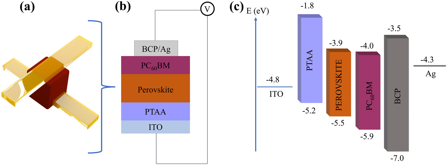 | ||
| Fig. 1 MemPVCell schematic structure and energy bands. (a) Schematic illustration of the MemPVCell device having an inverted PSC structure and (b) consisting of a glass/ITO/PTAA/Perovskite/PC60BM/BCP/Ag material stack. (c) Graphic representation of the layer's energy diagram. | ||
Steady state photovoltaic characterization of MemPVCell devices
The photovoltaic performance of the MemPVCell device was initially evaluated prior to performing memristive switching measurements. Fig. 2 and the corresponding tables show typical J–V characteristics and corresponding extraction of the photovoltaic parameters of 30 MemPVCell-1 and 30 MemPVCell-2 (thus with and without BCP, respectively). The statistical variation of power conversion efficiency (PCE), fill factor (FF), short circuit current (Jsc) and open circuit voltage (Voc) of 30 devices of each set is depicted in Fig. 2. The J–V curves and photovoltaic parameters of the champion devices are shown in Fig. 3. MemPVCell-1 devices exhibit an average PCE of 17.07% (champion PCE = 17.97%), while devices without BCP (MemPVCell-2) demonstrate a lower PCE of 15.35% (champion PCE = 16.26%). The main limiting factor of MemPVCell-2 is reported to be the lower FF value associated with the less Ohmic contact between Ag and PCBM in the absence of BCP – an insulating layer that helps in avoiding related Schottky barriers at metal semiconductor interfaces.32,33 Despite the lower PCE of MemPVCell-2 devices, the absence of BCP is reported to be beneficial for the memristive switching properties, which will be shown later in the manuscript.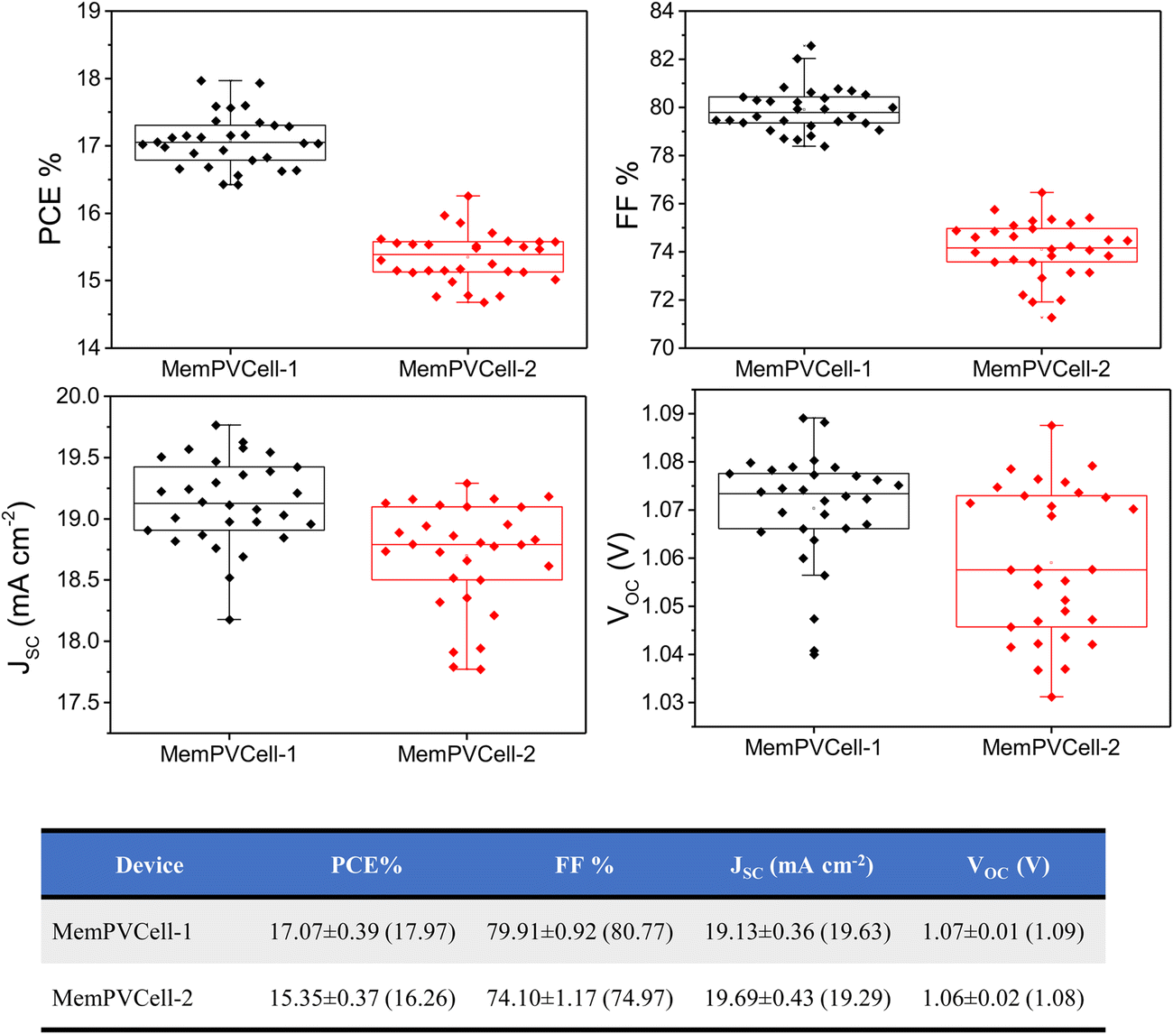 | ||
| Fig. 2 Extraction of the photovoltaic parameters of the multiple MemPVCell-1 and MemPVCell-2 devices. Statistical variation of power conversion efficiency (PCE), fill factor (FF), short circuit current (Jsc) and open circuit voltage (Voc) of 30 devices of each set. | ||
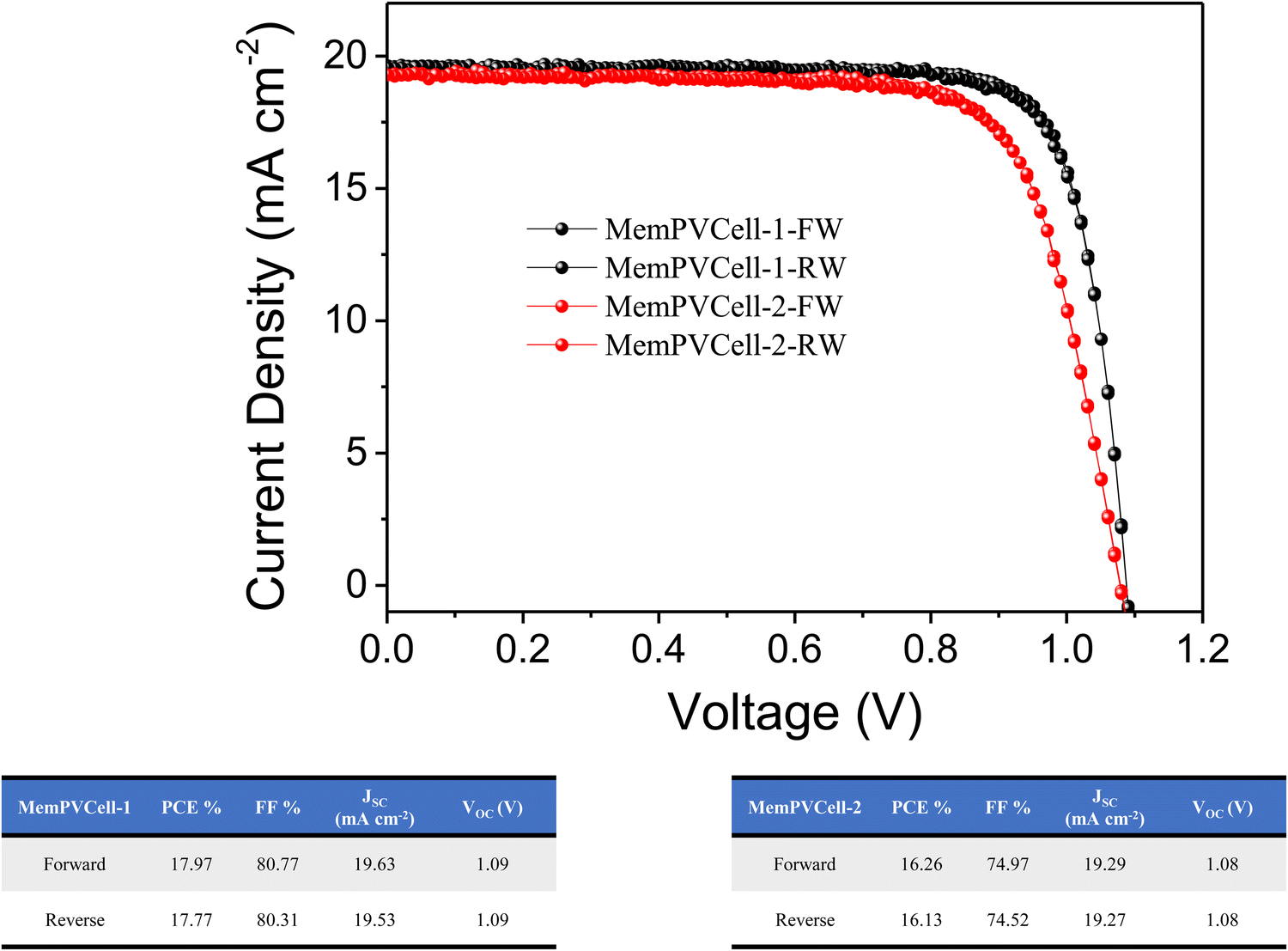 | ||
| Fig. 3 J–V curves and photovoltaic parameters of champion devices of MemPVCell-1 and MemPVCell-2 for reverse and forward scan directions. | ||
Transient photovoltaic characterization of MemPVCell
Transient photovoltage (TPV), TPC, Photo-CELIV and EQE measurements were performed in a typical MemPVCell-1 device and plotted in Fig. S1–S4 (ESI†), respectively. Small perturbation TPV decays followed a single exponential trend, which can result from either a charge carrier annihilation or a three-body recombination. Since the excitons in perovskites dissociate after 2 ps upon generation and our measurement covers a μs-scale, we can safely disregard the potential exciton contribution.32,33 Hence, the measured decay curves are the consequence of the electron–hole recombination, and the transient tail can directly yield the carrier lifetimes. The carrier lifetimes (∼5 μs) were extracted from the corresponding transient tail of TPV decay curves (Fig. S1, ESI†) that follow a single exponential trend.The TPC measurements were performed in a high perturbation regime (0.8 duty cycle) and show the absence of deep trap states in all the tested samples (Fig. S2, ESI†). The drift mobility of electrons/holes was probed using charge extraction by linearly increasing voltage (photo-CELIV) at various light pulse delay points. Furthermore, the drift mobility was derived from the extracted charge represented by the part of the transient superimposed over the displacement current level (Fig. S3, ESI†). Taking into account the fact that perovskites are not highly disordered materials and according to the equation proposed by Lorrmann et al., mobility can be derived:57
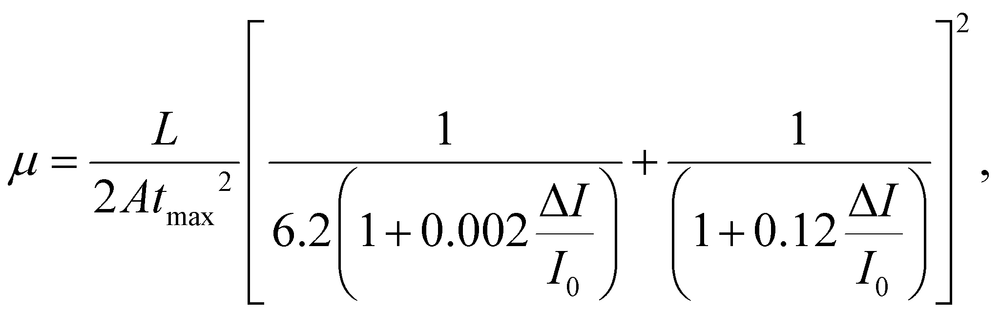
Fig. S4 (ESI†) shows the EQE spectrum of a typical device together with the calculated current density, which matches the Jsc value extracted from J–V curves. Fig. S5 (ESI†) depicts typical EIS data of MemPVCell-1 before the formation of a memristive channel, at different direct current (dc) biases varying from 0 to 1 V, while sweeping the frequency from 100 Hz to 1 MHz. In all cases, standard EIS arcs appear showing that the series resistance decreases as the dc bias increases. In the next section, we will discuss EIS data in the HRS and LRS after forming the memristive channel.
Resistance switching characteristics of MemPVCell devices
Fig. 4 shows dc voltage sweeps of the MemPVCell-1 device by varying the memristive channel forming process by setting different values of compliance current, Icc (1 and 10 mA).27,35 Moreover, different voltage scanning rates (10 mV s−1, 50 mV s−1, 100 mV s−1) were tested to identify how these parameters affect the Vset and Vreset values as well as the ON/OFF ratio (Table 1).35 The memristive channel in a pristine sample was achieved by applying a positive voltage exceeding the required threshold of ∼2 V. The dc voltage was applied to the Ag top electrode, while the ITO bottom electrode was grounded for all relevant measurements.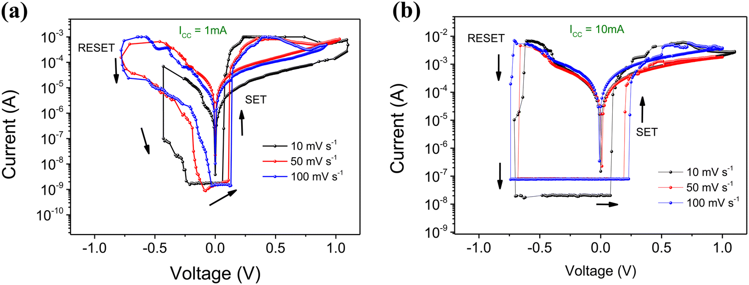 | ||
| Fig. 4 Influence of the scan rate and compliance current on resistive switching of MemPVCell-1. Switching memristive characteristics of MemPVCell-1 by sweeping the dc bias from −1 to 1 V at different scanning rates (10 mV s−1, 50 mV s−1, 100 mV s−1) and compliance current applied [1 mA (a) and 10 mA (b)]. | ||
| Scan rate (mV s−1) | V set (V) | V reset (V) | On/off ratio |
|---|---|---|---|
| I cc = 10 mA | |||
| 10 | 0.09 ± 0.01 | −0.58 ± 0.02 | 9.9 × 10⁴ |
| 50 | 0.19 ± 0.06 | −0.66 ± 0.05 | 2.5 × 10⁴ |
| 100 | 0.22 ± 0.03 | −0.71 ± 0.04 | 8.5 × 10⁴ |
| I cc = 1 mA | |||
| 10 | 0.07 ± 0.01 | −0.47 ± 0.05 | 1.0 × 10⁴ |
| 50 | 0.09 ± 0.01 | −0.69 ± 0.09 | 8.0 × 10³ |
| 100 | 0.12 ± 0.02 | −0.79 ± 0.04 | 5.2 × 10³ |
Stable bipolar resistive switching loops were obtained for each tested condition with an ON/OFF ratio ranging from 103 to 105, while a low (∼100–200 mV) positive voltage, Vset, results in HRS to LRS transition. The HRS is restored upon exceeding a moderate (∼700 mV) negative voltage threshold, Vreset. Table 1 summarizes the MemPVCell-1's ON/OFF ratio, Vset and Vreset dependence on scanning rate and Icc. The general trend is that Vset and Vreset increase as the scanning rate or Icc increases with a bigger influence on Vreset.35 The ON/OFF ratio also increases at high Icc values, reaching a value up to 105. Targeting the high ON/OFF ratio, initial high barriers between the active layer and the electrodes are reported in the majority of HP-based memristors34–38 by avoiding the insertion of electron and hole transport layers in the structure. Although this is the route of memristive performance improvement, however at a cost of high power and voltage operation, these energy barriers also render these structures incompatible with efficient solar energy harvesting.
Fig. 5 presents the statistical distribution of 15 different MemPVCell-1 and 15 different MemPVCell-2 devices measured at the scanning rate and Icc of 10 mV s−1 and 10 mA, respectively. It is apparent that MemPVCell-1 devices compared to MemPVCell-2 devices exhibit a slightly higher Vset (∼0.15 ± 0.06 V compared to 0.13 ± 0.04 V) while having a slightly lower Vreset (−0.65 ± 0.10 V compared to −0.75 ± 0.06 V). Overall, MemPVCell-2 exhibits less variation in resistive switching voltages measured among multiple cells of the same type (Table S4, ESI†). Fig. S6 (ESI†) depicts up to 125 consecutive dc resistance switching loops for both MemPVCell-1 (Fig. S6a, ESI†) and MemPVCell-2 (Fig. S6b, ESI†) devices revealing that both devices have excellent resistance state stability.
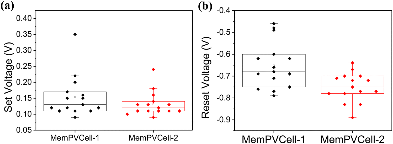 | ||
| Fig. 5 Resistive switching voltage statistics for 15 MemPVCell-1 (black data) and 15 MemPVCell-2 devices (red data). MemPVCell-1 devices exhibit a slightly higher Vset while having a slightly lower Vreset compared to MemPVCell-2. Icc = 10 mA and a scanning rate of 10 mV s−1 were used. | ||
Mechanism and light tuning of resistance switching characteristics
After analyzing the DC resistive switching behavior of the MemPVCell devices, it is crucial to examine whether the underlying mechanism responsible for the resistive switching is filament-based (either Ag or VI migration) or interface-dominated. The proposed mechanism for MemPVCell is the formation/rupture of VI enabled filaments,40,41,44,45 which is based on two arguments: the first argument lies in the abrupt increase/decrease of current by orders of magnitude after exceeding the switching threshold (SET/RESET process), under DC voltage sweeps. Nevertheless, this argument only precludes the interfacial switching case and cannot distinguish whether the filament originates in Ag or halide vacancies in the perovskite active layer or if it is a combination of both. The second argument is presented in Fig. 6. In this measurement, consecutive identical pulses of increasing light illumination were applied to the as-formed MemPVCell-1 device. In Fig. 6(a), consecutive pulses of 1 V amplitude and 10 ms width were applied for light intensities of 8, 16, 25, 40, 60 and 80 mW cm−2, respectively. The resistance of MemPVCell-1 increases with increasing light intensity and eventually approaches the HRS, indicating the rupture of VI filaments enabled by photo-induced halide (iodine) redistribution.44,45 Increasing the pulse width (1 V, 100 ms) as shown in Fig. 6(b) minimizes the light induced resistance enhancement although it cannot prevent the device resistance to increase approaching 1000 Ohm. On the other hand, increasing the pulse amplitude at 2 V (width either 10 ms, Fig. 6(c), or 50 ms, Fig. 6(d)) does have a stronger impact on the device LRS by setting its initial value below 100 Ohm under dark conditions (in contrast with the 1 V pulse case where the LRS under dark conditions is about 300 Ohm). It should be noted that even under 76 mW cm−2 light illumination, the LRS value lies around 300 Ohm. Overall, the higher pulse amplitude leads to the formation of a stronger filament and thus a lower LRS value (both under dark and light conditions), a situation that opposes the rupture of VI filaments and compensates for the effect of light on the active layer. Finally, increasing the pulse width from 10 ms to 50 ms under the same amplitude of 2 V further stabilizes the LRS to lower values while making its light tunability range lie between 70 and 130 Ohm under the dark and 76 mW cm−2, respectively. This light controlled LRS value could open the path for analogue computing processes apart from digital neuromorphic circuit applications. A similar behavior was observed in the case of MemPVCell-2.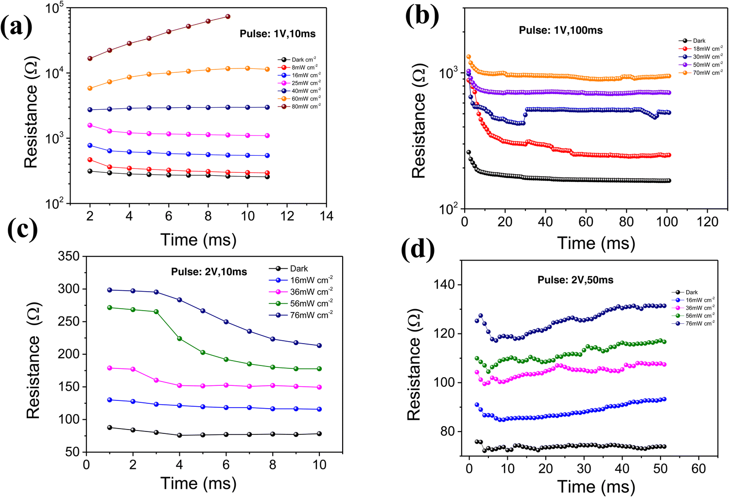 | ||
| Fig. 6 Light tuning of the resistance state of MemPVCell-1 under different illumination and electric pulse conditions. An electric pulse of the amplitude and duration of (a) 1 V, 10 ms, (b) 1 V, 100 ms, (c) 2 V, 10 ms, and (d) 2 V, 50 ms was applied to set the sample close to the LRS. Light illumination was varied from dark conditions up to 80 mW cm−2. | ||
We then investigated the effect of light illumination on the DC resistive switching of MemPVCell-1. Corresponding dc switching measurements under the light illumination of 50 mW cm−2 are presented in Fig. S7 (ESI†). Table S5a (ESI†) also shows the Vset and Vreset values for light intensities of 8 and 16 mW cm−2. It should be noted that under light, the Vset increases while the Vreset becomes less negative, indicating that light-generated carriers prevent the transition from the HRS to LRS while assisting the opposite transition from the LRS to HRS enabled by a light-modulated carriers’ barrier.40,42,58,59 The same trend is evident in Table S5b (ESI†), showing the dependence of Vset and Vreset as a function of scan rate. As the scan rate decreases, the set voltage significantly decreases, meaning that prolonged light illumination assists the reset process and the rupture of VI filaments. Similarly, the set voltage is reduced for the decreasing scan rate, as the prolonged electric field application reduces the switching threshold to the LRS under illumination. Our results are in agreement with photo-induced iodide redistribution44 and annihilation of Frenkel defects45 that were shown to lead to current suppression under light illumination in HP memristors.60 In particular, these measurements verify the existence of iodine filaments as the primary mechanism responsible for resistive switching, indicating that the increase/decrease of device conductance is attributed to the increase/decrease of  concentration. Contribution from Ag migration also cannot be excluded. A similar behavior was observed for the case of MemPVCell-2.
Finally, we have investigated how the EIS spectra are affected (Fig. S8, ESI†) by applying a dc bias and sweeping it across the Vset threshold of ∼150 mV. The sample is initialized in the HRS at zero bias, while when the bias is above 0.1 V, a transition from an arch-shaped spectrum to an almost vertical line is observed indicating a gradual transition to the LRS.61
Endurance and retention characteristics of MemPVCell devices
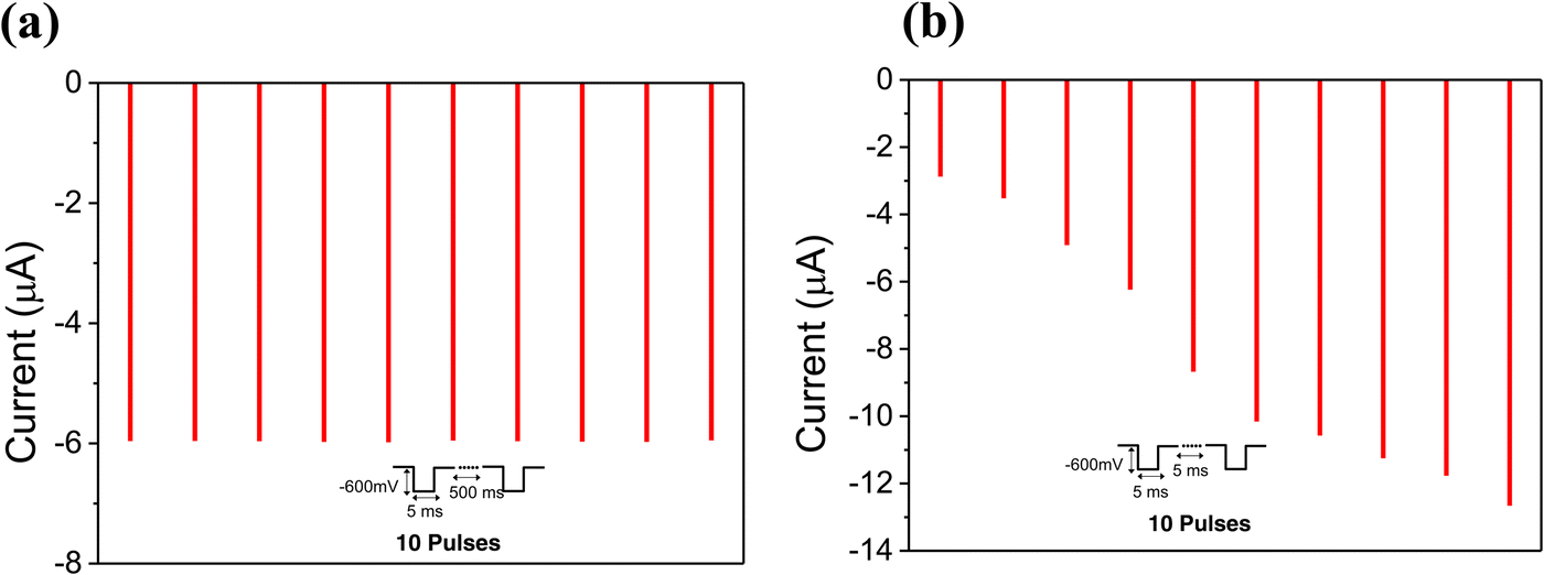
To investigate further the HRS and LRS stability, we implemented standard state endurance and retention measurements using ac pulses for both types of samples.24–28Fig. 7 depicts thousands of HRS to LRS cycling loops, indicating the overall high endurance of MemPVCell-1 and -2 devices. For these measurements, we used a large number of ac pulses up to 3 × 10³ cycles having the pulse amplitude of ±1 V and the duration of 100 ms. Both devices exhibit a zero change in the HRS/LRS ratio even after 3 × 10³ switching cycles. The purple shadow around the data points reflects the variation of thousands of switching pulses, revealing the high stability of the HRS and LRS under fast ac excitations. For the specific pulses’ configuration, MemPVCell-1 shows an initial HRS/LRS ratio of ∼103, while MemPVCell-2 has a value of ∼104, indicating the beneficial role on switching characteristics when BCP is not included in the structure. This is directly related to the development of Schottky barriers when BCP is absent in the device that results in less current conduction and thus higher HRS values. Overall, the high endurance of MemPVCell devices is likely to be linked to the multi-cation nature of the quadruple perovskite and especially to the beneficial role of Rb and the suppressed MA contribution.41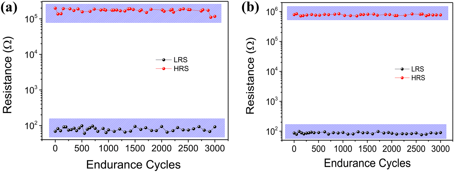 | ||
| Fig. 7 Cycling endurance of (a) MemPVCell-1 and (b) MemPVCell-2. The following pulse settings were used: number of pulses up to 3 × 10³, amplitude ±1 V, pulse duration 100 ms. For resistance reading, a pulse with the amplitude of ± 10 mV and the duration of 10 ms was used. | ||
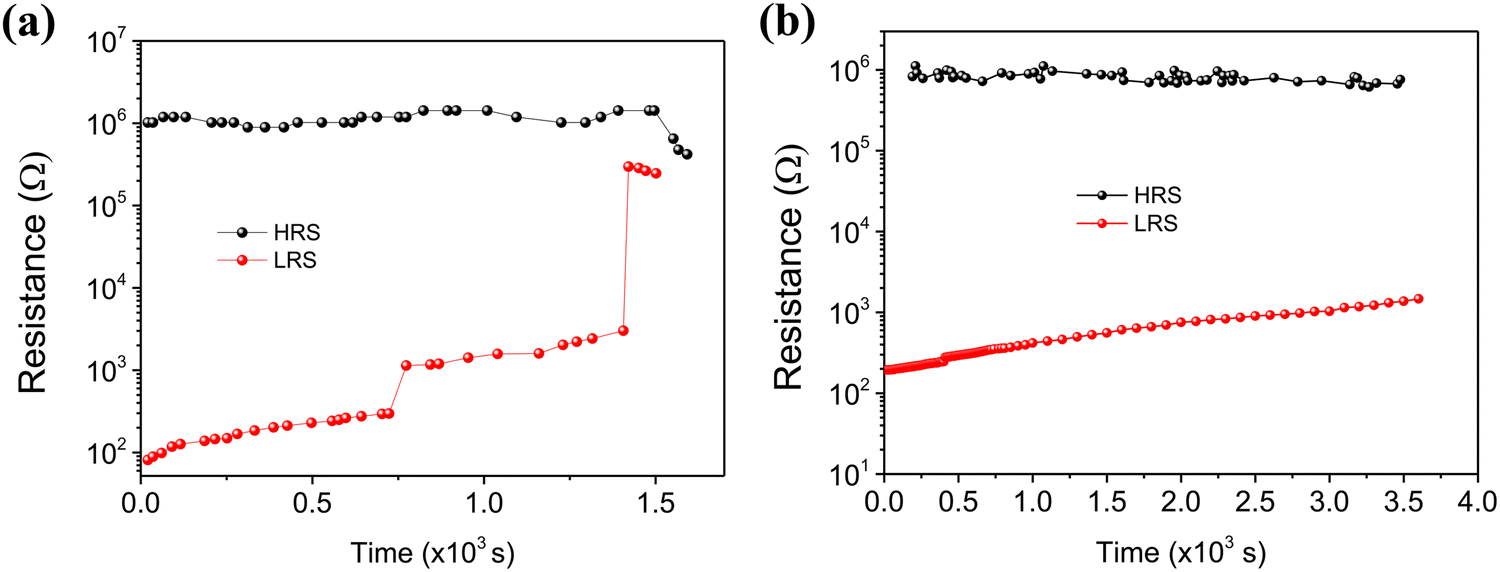
Moreover, retention characteristics of the HRS and LRS for both MemPVCell-1 and -2 are presented in Fig. 8. The initial HRS was set by applying a pulse with the amplitude of −1 V and the duration of 100 ms, while the LRS was set by applying a pulse with the amplitude of +1 V. The HRS demonstrates a superior retention showing no change even after 3500 s for both types of sample. On the other hand, the LRS exhibits a gradual increase in the initial value (∼200 Ohm) with time. In the case of MemPVCell-1, after ∼1300 s, we observed a sudden permanent switch from the LRS to the HRS. Notably, MemPVCell-2 exhibits a much better stability of LRS with time, resulting in a 30% resistance increase after 3500 s. Overall, the HRS/LRS ratio of MemPVCell-2 depicts a retention of more than 70% of its initial value, while MemPVCell-1 retains only 10% of its initial value after 3500 s. Therefore, the MemPVCell-2 device structure offers a much-improved LRS retention behaviour that also results in higher HRS/LRS ratio retention. The retention of MemPVCell-1 was also studied for ±2 V pulse amplitude. In this case, the on/off ratio reduced to 100, compared to the 1 V case. The results are shown in Table S6 (ESI†).
 | ||
| Fig. 8 Resistance state retention of (a) MemPVCell-1 and (b) MemPVCell-2. The following pulse settings were used: amplitude ±1 V and pulse duration 500 ms. For resistance reading, a pulse with the amplitude of ±20 mV and the duration of 10 ms every 5 s was used. | ||
Correlation between PCE performance and memristive switching
The key advantage of the proposed MemPVCell structure is the ability to use the same material stack for parallel solar energy harvesting and neuromorphic computation tasks going beyond von Neumann architectures. To investigate how the initial PCE performance of the MemPVCell device prior to memristive channel formation is affected by the resistance switching loops, we have plotted in Fig. 9(a), corresponding characteristics in pristine cells, after 50 and 100 switching loops for both MemPVCell-1 and MemPVCell-2. After 100 consecutive dc switching loops, the PCE of MemPVCell-1 remains at 92% of its initial value, whereas MemPVCell-2 retains 96% its PCE value even after 125 switching loops. For both samples, the stressful process of memristive switching loops did not affect the PCE performance significantly, while MemPVCell-2 exhibits a faster recovery process. To investigate how the ac switching excitations also affect the PCE performance, as shown in Fig. 9(b) we plot how the PCE of the MemCell-1 device is recovered with time after pulsed endurance tests. In particular, we continuously monitor the PCE of the device over time after performing 3000 endurance cycles. We report that the PCE is significantly dropped immediately after these stressful excitations, however a quick recovery is observed within a timeframe of a few minutes.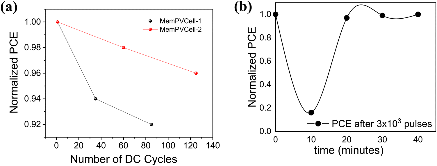 | ||
| Fig. 9 (a) Correlation between the PCE and number of dc resistance switching loops for MemPVCell-1 and MemPVCell-2 devices. For the loops, dc scans from −1 to 1 V using Icc = 10 mA and a scanning rate of 100 mV s−1 were used. (b) PCE recovery after pulsed endurance tests of the MemPVCell-1 device. The following pulse settings were used: number of pulses 3 × 10³, amplitude ±1 V, pulse duration 100 ms. For resistance reading, a pulse with the amplitude of −10 mV and duration of 10 ms was used. | ||
Neuromorphic behavior of MemPVCell devices
To validate further the memristive performance of the MemPVCell device, we measured basic synaptic functionalities by applying potentiation and depreciation pulse protocols under different pulse and light illumination conditions (Fig. 10(a) and (b)) as well as measured STP/LTP effects.10–15,24–28 For the potentiation and depreciation protocols under dark conditions, and when the memristor is set close to the LRS (Fig. 10(a)), we used a sequence of 50 pulses with the amplitude of 300 mV and 50 pulses at −300 mV with a duration of 10 ms each. During the first positive 50 pulses, a continuous increase of current is reported, while during the rest 50 negative pulses, the opposite behaviour is observed in line with potentiation and depreciation of conventional memristors.24–28 For the measurements shown in Fig. 10(b), we applied 30 pulses at +700 mV and 30 pulses at −600 mV with the duration of 1 ms each pulse at different light illuminations of 25–50 mW cm−2 (Fig. 10(b)). Light excitation results in enhanced current amplitude following an almost linear dependence.26,27 In Fig. 10(c), we demonstrate typical STP and LTP synaptic behaviours by implementing specific train pulses, while the device is initialized in the HRS. For the STP process, 4 consecutive pulses of 100 mV amplitude and 2 ms of duration were applied, while the current is afterwards recorded in time. This train of moderate pulses results in an initial increase of current (∼10 μA) for a period of 100 s, whereas afterwards the device is spontaneously switched back to the HRS. In contrast, by applying 5 consecutive pulses of 700 mV in amplitude and 5 ms in duration, we observed the direct transition of the sample to the LRS and its stability in this state for a period of 400 s, demonstrating therefore a LTP process. As a demonstration of mimicking a spike-timing dependent plasticity (STDP) based on MemPVCell, as shown in Fig. 11, the effect of a train of 10 pulses (−600 mV amplitude, 5 ms duration) on the synaptic current is depicted with different time intervals between them being either 500 ms (Fig. 11(a)) or 5 ms (Fig. 11(b)). In the case the pulses are well-separated in time, no effect on current is reported. On the other hand, when the time interval is within few ms, a clear STDP effect is observed, resulting in a 4× enhancement of synaptic current.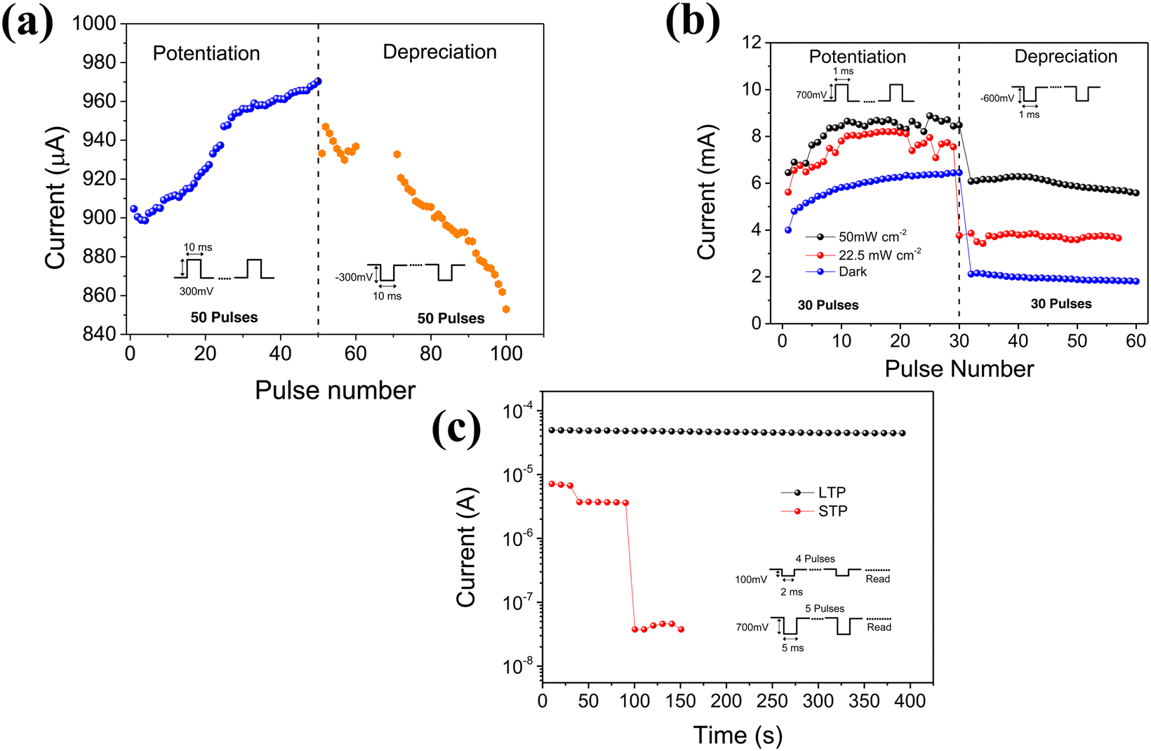 | ||
| Fig. 10 Basic synaptic functionalities of MemPVCell-1. Potentiation and depreciation pulse protocols under (a) dark (50 pulses at ±300 mV with the duration of 10 ms each pulse), and (b) illumination conditions. In panel (b), for dark and all light conditions, we used 30 pulses at 700 mV and −600 mV for 1 ms, (c) short-term (STP) and long-term (LTP) plasticity measurements. For LTP: 5 pulses, 700 mV 5 ms, read at 10 mV every 10 s, and for STP, 4 pulses, 100 mV for 2 ms, read at −20 mV every 10 s were used. | ||
 | ||
| Fig. 11 Mimicking the spike-timing dependent plasticity (STDP) using a MemPVCell-1 device for 10 identical applied pulses (−600 mV of amplitude, 5 ms of duration) of (a) 500 ms and (b) 5 ms interval. | ||
Routes towards further device performance improvement were investigated by modifying the layer components of the MemPVCell-1 structure. In particular, we prepared samples without including the PCBM layer, termed as MemPVCell-3 (Fig. S9, ESI†), and samples without including the PTAA layer termed as MemPVCell-4 (Fig. S10, ESI†). In both cases, the memristive performance was worse compared to MemPVCell-1 and -2, while the PCE performance was significantly suppressed (PCE less than 5%) – as expected in a PSC structure without an electron transport layer (MemPVCell-3) or without a hole transport layer (MemPVCell-4). MemPVCell-3 required higher Vset and Vreset pulses, while the HRS/LRS ratio is reported to be 2 orders of magnitude less compared to MemPVCell-1 and MemPVCell-2. Notably to mention, only very few devices of the same batch exhibited memristive switching characteristics. MemPVCell-4 required high switching voltages, while only a few devices were operational (this is probably attributed to the low perovskite quality when coated on ITO instead of the PTAA layer), despite the good stability of the working devices.
Conclusions
In this study, we demonstrated that is possible to use a an efficient inverted PSC structure based on a quadruple cation-based perovskite (this is the first memristor realization based on quadruple cation perovskites at least to the best of the authors’ knowledge), and implement, using the same material stack, parallel solar energy harvesting and memristive functionalities. We show that a PSC with an average PCE of ∼17% is capable, upon appropriate memristive channel formation, to demonstrate stable resistance switching characteristics without losing its PCE performance even after multiple dc or thousands of ac switching cycles. In particular, the MemPVCell demonstrates the HRS to LRS ratio of up to 105 and fast and light-tuneable switching cycles with the endurance of 3 × 10³ with no detectable HRS/LRS ratio drop. Overall, an HRS/LRS ratio retention of up to 3600 s with less than a 30% drop in its initial value was also shown for MemPVCell-2. The corresponding PCE performance was also monitored after the implementation of multiple resistance switching loops and endurance cycles, indicating that a full PCE recovery to the device's initial value is attainable within a few minutes of rest. Aiming at further improving the device performance, modifications in the MemPVCell's layered structure were investigated, a process that allowed identification of the impact of each layer on the parallel photovoltaic and memristive switching characteristics. This process suggests that the interfaces between the perovskite and PCBM, as well as PCBM and Ag contact, are vital for the overall good performance of the MemPVCell device. On-going experiments focus on developing novel interfacial engineering routes and are expected to allow achieving much better memristive performance (increasing HRS/LRS ratio, endurance, and retention) without sacrificing the PCE performance.Conflicts of interest
There are no conflicts to declare.Acknowledgements
The work has been supported by the European Union's Horizon 2020 research and innovation program under project EMERGE. The EMERGE project has received funding under grant agreement no. 101008701.Notes and references
- S. Bains, Nat. Electron., 2020, 3, 348–351 CrossRef.
- Wm. A. Wulf and S. A. McKee, Comput. Archit. News, 1995, 23, 20–24 CrossRef.
- M. A. Zidan, J. P. Strachan and W. D. Lu, Nat. Electron., 2018, 1, 22–29 CrossRef.
- Smart Sensors at the IoT Frontier, ed. H. Yasuura, C.-M. Kyung, Y. Liu and Y.-L. Lin, Springer International Publishing, Cham, 2017 Search PubMed.
- Q. Xia and J. J. Yang, Nat. Mater., 2019, 18, 309–323 CrossRef CAS PubMed.
- F. Zhou, Z. Zhou, J. Chen, T. H. Choy, J. Wang, N. Zhang, Z. Lin, S. Yu, J. Kang, H.-S. P. Wong and Y. Chai, Nat. Nanotechnol., 2019, 14, 776–782 CrossRef CAS PubMed.
- F. Cai, J. M. Correll, S. H. Lee, Y. Lim, V. Bothra, Z. Zhang, M. P. Flynn and W. D. Lu, Nat. Electron., 2019, 2, 290–299 CrossRef CAS.
- R. Berdan, T. Marukame, K. Ota, M. Yamaguchi, M. Saitoh, S. Fujii, J. Deguchi and Y. Nishi, Nat. Electron., 2020, 3, 259–266 CrossRef.
- S. Nau, C. Wolf, S. Sax and E. J. W. List-Kratochvil, Adv. Mater., 2015, 27, 1048–1052 CrossRef CAS PubMed.
- P. C. Harikesh, B. Febriansyah, R. A. John and N. Mathews, MRS Bull., 2020, 45, 641–648 CrossRef.
- Y. Tuchman, T. N. Mangoma, P. Gkoupidenis, Y. van de Burgt, R. A. John, N. Mathews, S. E. Shaheen, R. Daly, G. G. Malliaras and A. Salleo, MRS Bull., 2020, 45, 619–630 CrossRef.
- Y. van de Burgt, A. Melianas, S. T. Keene, G. Malliaras and A. Salleo, Nat. Electron., 2018, 1, 386–397 CrossRef.
- J. Y. Gerasimov, D. Zhao, A. Sultana, T. Abrahamsson, S. Han, D. Bliman, D. Tu, D. T. Simon, R. Olsson, X. Crispin, M. Berggren and S. Fabiano, Adv. Electron. Mater., 2021, 7, 2001126 CrossRef CAS.
- D. D. A. Koutsouras, T. Prodromakis, G. G. Malliaras, P. W. M. Blom and D. P. Gkoupidenis, Adv. Intell. Syst., 2019, 1, 1900013 CrossRef.
- F. Torricelli, D. Z. Adrahtas, Z. Bao, M. Berggren, F. Biscarini, A. Bonfiglio, C. A. Bortolotti, C. D. Frisbie, E. Macchia, G. G. Malliaras, I. McCulloch, M. Moser, T.-Q. Nguyen, R. M. Owens, A. Salleo, A. Spanu and L. Torsi, Nat. Rev. Methods Primers, 2021, 1, 66 CrossRef CAS PubMed.
- G. Kakavelakis, M. Gedda, A. Panagiotopoulos, E. Kymakis, T. D. Anthopoulos and K. Petridis, Adv. Sci., 2020, 7, 2002098 CrossRef CAS PubMed.
- G. Kakavelakis, E. Gagaoudakis, K. Petridis, V. Petromichelaki, V. Binas, G. Kiriakidis and E. Kymakis, ACS Sens., 2018, 3, 135–142 CrossRef CAS PubMed.
- C.-X. Zhang, T. Shen, D. Guo, L.-M. Tang, K. Yang and H.-X. Deng, InfoMat, 2020, 2, 1034–1056 CrossRef CAS.
- Q. Liao, X. Jin and H. Fu, Adv. Opt. Mater., 2019, 7, 1900099 CrossRef.
- H. Wang and D. H. Kim, Chem. Soc. Rev., 2017, 46, 5204–5236 RSC.
- X. Liu, D. Yu, X. Song and H. Zeng, Small, 2018, 14, 1801460 CrossRef PubMed.
- K. Rogdakis, N. Karakostas and E. Kymakis, Energy Environ. Sci., 2021, 14, 3352–3392 RSC.
- Z. Fan, K. Sun and J. Wang, J. Mater. Chem. A, 2015, 3, 18809–18828 RSC.
- X. Xiao, J. Hu, S. Tang, K. Yan, B. Gao, H. Chen and D. Zou, Adv. Mater. Technol., 2020, 5, 1900914 CrossRef CAS.
- G. Cao, C. Cheng, H. Zhang, H. Zhang, R. Chen, B. Huang, X. Yan, W. Pei and H. Chen, J. Semicond., 2020, 41, 051205 CrossRef CAS.
- R. A. John, N. Shah, S. K. Vishwanath, S. E. Ng, B. Febriansyah, M. Jagadeeswararao, C.-H. Chang, A. Basu and N. Mathews, Nat. Commun., 2021, 12, 3681 CrossRef CAS PubMed.
- U. Das, P. Sarkar, B. Paul and A. Roy, Appl. Phys. Lett., 2021, 118, 182103 CrossRef CAS.
- Y. Fang, S. Zhai, L. Chu and J. Zhong, ACS Appl. Mater. Interfaces, 2021, 13, 17141–17157 CrossRef CAS PubMed.
- X. Zhao, H. Xu, Z. Wang, Y. Lin and Y. Liu, InfoMat, 2019, inf2.12012 CrossRef.
- M. Saliba, T. Matsui, K. Domanski, J. Y. Seo, A. Ummadisingu, S. M. Zakeeruddin, J. P. Correa-Baena, W. R. Tress, A. Abate, A. Hagfeldt and M. Grätzel, Science, 2016, 354, 206–209 CrossRef CAS PubMed.
- M. Petrović, K. Rogdakis and E. Kymakis, J. Phys. Energy, 2019, 1, 044001 CrossRef.
- D. Tsikritzis, K. Rogdakis, K. Chatzimanolis, M. Petrović, N. Tzoganakis, L. Najafi, B. Martín-García, R. Oropesa-Nuñez, S. Bellani, A. E. Del Rio Castillo, M. Prato, M. M. Stylianakis, F. Bonaccorso and E. Kymakis, Mater. Adv., 2020, 1, 450–462 RSC.
- K. Chatzimanolis, K. Rogdakis, D. Tsikritzis, N. Tzoganakis, M. Tountas, M. Krassas, S. Bellani, L. Najafi, B. Martín-García, R. Oropesa-Nuñez, M. Prato, G. Bianca, I. Plutnarova, Z. Sofer, F. Bonaccorso and E. Kymakis, Nanoscale Adv., 2021, 3, 3124–3135 RSC.
- E. J. Yoo, M. Lyu, J. H. Yun, C. J. Kang, Y. J. Choi and L. Wang, Adv. Mater., 2015, 27, 6170–6175 CrossRef CAS PubMed.
- Y. Huang, L. Tang, C. Wang, H. Fan, Z. Zhao, H. Wu, M. Xu, R. Shen, Y. Yang and J. Bian, ACS Appl. Electron. Mater., 2020, 2, 3695–3703 CrossRef CAS.
- X. F. Cheng, W. H. Qian, J. Wang, C. Yu, J. H. He, H. Li, Q. F. Xu, D. Y. Chen, N. J. Li and J. M. Lu, Small, 2019, 15, 1905731 CrossRef CAS PubMed.
- D. Liu, Q. Lin, Z. Zang, M. Wang, P. Wangyang, X. Tang, M. Zhou and W. Hu, ACS Appl. Mater. Interfaces, 2017, 9, 6171–6176 CrossRef CAS PubMed.
- W. H. Qian, X. F. Cheng, Y. Y. Zhao, J. Zhou, J. H. He, H. Li, Q. F. Xu, N. J. Li, D. Y. Chen and J. M. Lu, Adv. Mater., 2019, 31, 1806424 CrossRef PubMed.
- A. Pérez-Tomás, Adv. Mater. Interfaces, 2019, 6, 1900471 CrossRef.
- X. Zhu, J. Lee and W. D. Lu, Adv. Mater., 2017, 29, 1700527 CrossRef PubMed.
- S. Lee, J. Choi, J. B. Jeon, B. J. Kim, J. S. Han, T. L. Kim, H. S. Jung and H. W. Jang, Adv. Electron. Mater., 2019, 5, 1800586 CrossRef.
- X. Guan, W. Hu, M. Azimul Haque, N. Wei, Z. Liu, A. Chen, T. Wu, X. Guan, W. J. Hu, M. A. Haque, Z. Liu, A. Chen, T. Wu and N. Wei, Adv. Funct. Mater., 2018, 28, 1704665 CrossRef.
- S. Ham, S. Choi, H. Cho, S.-I. Na and G. Wang, Adv. Funct. Mater., 2019, 29, 1806646 CrossRef.
- D. W. deQuilettes, W. Zhang, V. M. Burlakov, D. J. Graham, T. Leijtens, A. Osherov, V. Bulović, H. J. Snaith, D. S. Ginger and S. D. Stranks, Nat. Commun., 2016, 7, 11683 CrossRef CAS PubMed.
- E. Mosconi, D. Meggiolaro, H. J. Snaith, S. D. Stranks and F. De Angelis, Energy Environ. Sci., 2016, 9, 3180–3187 RSC.
- X. Xiao, J. Hu, S. Tang, K. Yan, B. Gao, H. Chen and D. Zou, Adv. Mater. Technol., 2020, 5, 1–29 Search PubMed.
- A bioinspired optoelectronically engineered artificial neurorobotics device with sensorimotor functionalities|Nature Communications, https://www.nature.com/articles/s41467-019-11823-4, (accessed June 19, 2022).
- M. Lanza, H.-S. P. Wong, E. Pop, D. Ielmini, D. Strukov, B. C. Regan, L. Larcher, M. A. Villena, J. J. Yang, L. Goux, A. Belmonte, Y. Yang, F. M. Puglisi, J. Kang, B. Magyari-Köpe, E. Yalon, A. Kenyon, M. Buckwell, A. Mehonic, A. Shluger, H. Li, T.-H. Hou, B. Hudec, D. Akinwande, R. Ge, S. Ambrogio, J. B. Roldan, E. Miranda, J. Suñe, K. L. Pey, X. Wu, N. Raghavan, E. Wu, W. D. Lu, G. Navarro, W. Zhang, H. Wu, R. Li, A. Holleitner, U. Wurstbauer, M. C. Lemme, M. Liu, S. Long, Q. Liu, H. Lv, A. Padovani, P. Pavan, I. Valov, X. Jing, T. Han, K. Zhu, S. Chen, F. Hui and Y. Shi, Adv. Electron. Mater., 2019, 5, 1800143 CrossRef.
- Z. Xiao and J. Huang, Adv. Electron. Mater., 2016, 2, 1600100 CrossRef.
- Y. Fang, S. Zhai, L. Chu and J. Zhong, ACS Appl. Mater. Interfaces, 2021, 13, 17141–17157 CrossRef CAS PubMed.
- S. Gil Kim, Q. Van Le, J. Su Han, H. Kim, M.-J. Choi, S. A. Lee, T. Ludvic Kim, S. Bum Kim, S. Young Kim, H. Won Jang, S. G. Kim, J. S. Han, H. Kim, M. Choi, S. A. Lee, T. L. Kim, S. B. Kim, H. W. Jang, Q. Van Le, D. Nang and V. S. Y. Kim, Adv. Funct. Mater., 2019, 29, 1906686 CrossRef.
- A. Abnavi, R. Ahmadi, A. Hasani, M. Fawzy, M. R. Mohammadzadeh, T. De Silva, N. Yu and M. M. Adachi, ACS Appl. Mater. Interfaces, 2021, 13, 45843–45853 CrossRef CAS PubMed.
- S. Seo, S.-H. Jo, S. Kim, J. Shim, S. Oh, J.-H. Kim, K. Heo, J.-W. Choi, C. Choi, S. Oh, D. Kuzum, H.-S. P. Wong and J.-H. Park, Nat. Commun., 2018, 9, 5106 CrossRef PubMed.
- H. Xie, Z. Wang, Z. Chen, C. Pereyra, M. Pols, K. Gałkowski, M. Anaya, S. Fu, X. Jia, P. Tang, D. J. Kubicki, A. Agarwalla, H.-S. Kim, D. Prochowicz, X. Borrisé, M. Bonn, C. Bao, X. Sun, S. M. Zakeeruddin, L. Emsley, J. Arbiol, F. Gao, F. Fu, H. I. Wang, K.-J. Tielrooij, S. D. Stranks, S. Tao, M. Grätzel, A. Hagfeldt and M. Lira-Cantu, Joule, 2021, 5, 1246–1266 CrossRef CAS.
- A. Pérez-Tomás, A. Lima, Q. Billon, I. Shirley, G. Catalan and M. Lira-Cantú, Adv. Funct. Mater., 2018, 28, 1707099 CrossRef.
- A. Pérez-Tomas, H. Xie, Z. Wang, H.-S. Kim, I. Shirley, S.-H. Turren-Cruz, A. Morales-Melgares, B. Saliba, D. Tanenbaum, M. Saliba, S. M. Zakeeruddin, M. Gratzel, A. Hagfeldt and M. Lira-Cantu, Sustainable Energy Fuels, 2019, 3, 382–389 RSC.
- J. Lorrmann, B. H. Badada, O. Inganäs, V. Dyakonov and C. Deibel, J. Appl. Phys., 2010, 108, 113705 CrossRef.
- F. Zhou, Y. Liu, X. Shen, M. Wang, F. Yuan and Y. Chai, Adv. Funct. Mater., 2018, 28, 1800080 CrossRef.
- S.-Y. Cai, C.-Y. Tzou, Y.-R. Liou, D.-R. Chen, C.-Y. Jiang, J.-M. Ma, C.-Y. Chang, C.-Y. Tseng, Y.-M. Liao, Y.-P. Hsieh, M. Hofmann and Y.-F. Chen, ACS Appl. Mater. Interfaces, 2019, 11, 4649–4653 CrossRef CAS PubMed.
- X. Zhu and W. D. Lu, ACS Nano, 2018, 12, 1242–1249 CrossRef CAS PubMed.
- C. Gonzales, A. Guerrero and J. Bisquert, Appl. Phys. Lett., 2021, 118, 073501 CrossRef CAS.
Footnote |
| † Electronic supplementary information (ESI) available: Extra memristive switching and PV characteristics under different electrical and illumination conditions; transient photovoltage (TPV) and transient photocurrent (TPC), photo-Celiv, external quantum efficiency (EQE) spectra, electrochemical impedance spectroscopy (EIS). See DOI: https://doi.org/10.1039/d2ma00402j |
| This journal is © The Royal Society of Chemistry 2022 |