DOI:
10.1039/D2MA00317A
(Paper)
Mater. Adv., 2022,
3, 5922-5929
NiO-GDC nanowire anodes for SOFCs: novel growth, characterization and cell performance†
Received
20th March 2022
, Accepted 3rd June 2022
First published on 6th June 2022
Abstract
A solid-oxide fuel cell (SOFC) is a sustainable energy resource that has been efficiently used for large-scale applications such as gas-turbines. However, its miniaturization for small-scale applications requires novel electrode materials especially anodes (other than Ni-YSZ) in different configurations and designs such as in the nanostructure form. Herein, we are proposing the growth of a novel nickel oxide–gadolinium doped ceria (NiO-GDC) nanowire-based anode using a vapor–liquid–solid (VLS) mechanism. To the best of our knowledge, NiO-GDC has never been grown before in the form of nanowires using the VLS mechanism. The nanowires are prepared at different evaporation temperatures and exhibit dense morphology. Detailed Raman spectroscopy reveals that during the growth, reorganization of NiO-GDC particles results in the formation of a more complex structure that diverges from pristine NiO-GDC powder. Furthermore, the temperature-dependence of the electrical conductivity reveals that the nanowires prepared at 1400 °C (evaporation temperature) possess high conductivity due to better charge-carrier transport, confirmed by their low activation energies. The electrolyte-supported button cell synthesized using a NiO-GDC nanowire anode exhibits a maximum power density of ∼178 mW cm−2 at 800 °C and concentration polarization is found to be the major loss, as revealed by electrochemical impedance spectroscopy (EIS) data. Based on our preliminary investigations, these nanowires have great potential to be used as an anode for SOFCs.
Introduction
In the increasing demand for renewable energy resources due to worldwide industrial and technological developments, fuel cells (FCs) represent a class of technology which is efficient, clean, sustainable, secure and affordable.1–3 FCs are static energy conversion devices that produce electricity via an electrochemical reaction between a fuel and an oxidizing agent. There are six different kinds of FCs depending upon the electrolyte and the fuel such as alkaline fuel cells (AFCs), solid oxide fuel cells (SOFCs), direct methanol fuel cells (DMFCs) and others.4 Among them, SOFCs are highly efficient and use a solid electrolyte such as dense yttria stabilized zirconia (YSZ) for their operation.5 Moreover, one of the major advantages of SOFCs is the possibility of utilizing different kinds of fuels such as hydrogen, hydrocarbons, carbon monoxide, etc.6 However, there are still several critical issues that need attention such as high operational temperature, slow start up and high cost. In particular, small-scale applications such as small electrical generators, micro-CPH (combined heat and power systems) and other portable electronic devices require novel electrode materials and designs that can be operated at relatively lower temperatures (lower than YSZ based SOFCs) and in turn produce high efficiency.7 For example, in the development of micro-SOFCs, major challenges that need to be overcome are bulky design and high temperature operation.7
In this regard, the nickel oxide–gadolinium doped ceria (NiO-GDC) anode and GDC electrolyte are attracting considerable attention for developing intermediate-temperature SOFCs (IT-SOFCs) due to their high conductivity at temperatures ranging from 500 °C to 650 °C and exceptional physical/chemical properties.8–11 Furthermore, for miniaturization, nanostructured materials can be the best option due to their exceptional physical/chemical properties such as compact size, a high surface to volume ratio, suitable transport properties, better electrical properties and so on.12 Among different nanostructure forms, nanowires (NWs) exhibit well-defined crystal orientation, single crystallinity and exceptional physical/chemical properties.13 Indeed, NWs also offer suitable morphology for the flow of fuel and oxidizing agents. Moreover, when developing layered structures like SOFCs, lattice matching between different layers plays an extremely important role especially in the mechanical properties of the device. It has been found that in nanowire (NW) morphology lattice mismatch strains can be relaxed elastically at the NW free surface without the formation of dislocations.14 This implies that the critical thickness is much greater in the NW morphology as compared to other structures such as thin films. Hence, this property of NWs to combine materials regardless of any need for lattice-matching can be explored in SOFC devices.
Herein, we propose novel NiO-GDC nanowires synthesized via the vapor liquid solid (VLS) mechanism in a tubular furnace for their application as an anode material for SOFCs. NWs were grown at two different evaporation temperatures and the deposition time was kept constant. To the best of our knowledge, NiO-GDC has never been grown before in the form of nanowire morphology especially using the VLS mechanism. Indeed, VLS is a high yield technique and is immensely used for nanowire growth due to its many advantages such as direct growth on an active substrate, no requirement for precursors, and lowered reaction energy and because it only needs a furnace and primary pumping system.15 The nanowires were characterized to investigate their surface morphology, structure and electrical properties via different characterization techniques. Finally, the nanowires were grown on a commercial single electrode (cathode only) button cell to investigate the cell and its electrochemical performance. Detailed investigations reveal that the NiO-GDC nanowires have the potential to be used as an anode for SOFCs.
Experimental
Substrate preparation
In this work, 3 × 3 and 10 × 10 mm2 alumina substrates (99% purity, Kyocera, Japan) were used to grow the NiO-GDC nanowires. Specifically, 10 × 10 mm2 alumina substrates were mainly used for structural characterization using nano-Raman spectroscopy, while 3 × 3 mm2 alumina substrates were employed for surface morphology and electrical studies. Prior to the growth, substrates were ultrasonically cleaned with acetone for 20 minutes and then dried with synthetic air. Afterward, a gold (Au) catalyst was deposited on the alumina substrates using RF-magnetron sputtering. The catalyst deposition was done at 70 watts with 7 sccm of argon (Ar) plasma for 5 seconds. The distance between the Au-target and the alumina substrate was fixed at 7.1 cm. The Au catalysts acted as nucleation sites for the growth of highly crystalline nanowires. Indeed, during the growth, these metal catalysts liquidized and when the supersaturation was reached, acted as a preferential site for the crystallization of nanowires.16 It should be pointed out that the middle area of the alumina substrate was exposed to Au-catalyst and the sides were masked for the deposition of Pt-contacts (see Fig. 1).
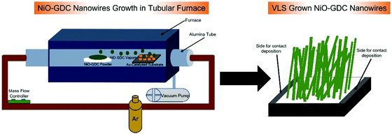 |
| | Fig. 1 Schematic representing the growth of NiO-GDC nanowires in a tubular furnace. | |
Growth of NiO-GDC nanowires using the VLS mechanism and characterization
NiO-GDC nanowire growth was performed in a lab-made tubular furnace equipped with vacuum pumps and heating systems by using the vapor liquid solid (VLS) mechanism. The VLS mechanism is named after the three different material phases involved in the process of nanowire growth i.e. vapor state of the source material, liquid catalyst droplets and solid crystalline nanostructures produced. The vacuum pump maintains a pressure of 10 mbar inside the alumina tube during the deposition. The NiO-GDC powder (fuelcellmaterials, 60% NiO and 40% GDC (Gd0.1Ce0.9O1.95)) was placed inside the furnace in the maximum temperature region to promote evaporation. In this work, the depositions were carried out at two different evaporation temperatures i.e. at 1400 °C and 1450 °C, while the deposition was carried out for 40 minutes. It should be pointed out that the selection of these temperatures was done after the optimization of nanowire formation. In particular, no evaporation of NiO-GDC powder was observed for the temperatures below 1400 °C and our furnace could reach only up to 1450 °C. For the deposition at 1400 °C, the substrates were placed in a relatively colder region of the furnace at 1120 °C, allowing the condensation in the form of nanowires. However, for nanowires deposited at 1450 °C, the substrates were placed at 1170 °C inside the tubular furnace. These substrate temperatures were selected after the optimization of nanowire growth conditions (see the ESI,† Fig. S1). An argon flow (set at 100 sccm) was used as the carrier gas transporting NiO-GDC particles from source materials to substrates during the deposition. First of all, the furnace was heated up to reach the desired deposition temperature (1400 °C and 1450 °C). In this stage the argon gas flow was maintained from the substrate to surface material direction to avoid any undesired deposition. When the furnace reached the deposition temperature, the argon flow was directed from the source to the substrate. Indeed, the VLS mechanism is named after the three different phases of the material involved in the growth process: the vapor state of the source material (NiO-GDC), the formation of the liquid catalyst droplet (Au), and the solid crystalline nanostructure that is produced.13 Hence, in the present case, the formation of a liquid droplet of a Au-catalyst occurs at the substrate temperature (1120 °C and 1170 °C) and NiO-GDC vapors adsorb on its surface. Since vapors are continuously provided, the liquid alloy starts to saturate forming a solid precipitate, which grows in the form of a 1D nanostructure.17 As can be seen from the above discussion, the metal-catalyst plays an extremely important role in the growth of nanowires. Indeed, catalysts need to fulfill certain important requirements i.e. they must be a liquid at the deposition temperature, they must be inert to chemical reactions, the vapor pressure of the catalyst component over the liquid alloy should be small, and they must not produce intermediate solids. For further details about the VLS mechanism for nanowire growth, the reader can refer to these review articles.13,18
The whole process of NiO-GDC NW growth is summarized in Fig. 1. The surface morphology of bare nanowires was examined using two different FE-SEM microscopes i.e. LEO 1525 (Gemini model; Carl Zeiss AG, Oberkochen, Germany) and MIRA 3 LMU (TESCAN, Brno, Czech Republic). The surface morphological images were acquired by operating the FE-SEM at 7 kV. Raman spectra were measured by using an XploRA Nano system (Horiba Jobin Yvon Srl, Italy) with a confocal microscope (Olympus BX) and a 1200 g mm−1 reticule. A Peltier-cooled Open Electrode CCD was used to record the Raman spectra excited by a 638 solid-state laser. Spectra were recorded in the wavelength range 100–1800 cm−1. The crystalline properties of bare NiO/GDC NWs were examined using the XRD technique (Empyrean diffractometer, PANalytical, the Netherlands). The XRD analysis was performed using Cu-LFF (λ = 1.5406 Å) operated at 40 kV and 40 mA in the diffraction angle range of 10–90°.
Device fabrication for electrical measurements
The devices for temperature dependent electrical measurements were prepared by using DC magnetron sputtering (sputtering parameters: power = 75 W, carrier gas: argon (7 sccm flow) and deposition pressure = 5.3 × 10⁻³ mbar). Again, the distance between the Au-target and the alumina substrate was fixed at 7.1 cm. Firstly, 50 nm thick adhesion layers of a titanium tungsten (TiW) alloy in the form of parallel pads were deposited on the sides of samples by using a shadow mask. The deposition was carried out for 3 minutes. Afterwards, 20 minutes deposition of platinum contacts (parallel pads, thickness: 1 μm) was carried out again by using a shadow mask with the same sputtering parameters. Furthermore, for temperature dependent electrical measurements, Pt heating elements were also deposited using a DC magnetron on the back side of the substrates. For this purpose, successive depositions of Pt pads (using a TiW adhesion layer) and a Pt heater were performed. The prepared devices were finally mounted on TO packages using electro-soldered gold wires. The whole process of device fabrication and a picture of the TO packaged NiO-GDC nanowire device are shown in Fig. 2.
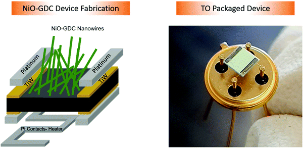 |
| | Fig. 2 Deposition of electrical contacts on NiO-GDC nanowires (left) and picture of the final TO packaged mounted device (right). | |
To investigate the electrical properties of nanowires, a custom-made stainless-steel climatic chamber was used. The conductance of the nanowires was investigated for temperatures ranging from 100 to 500 °C. The temperature of the devices was controlled by modulating the electric power applied to the heater using a Thurlby-Thandar PL_330DP power supply system. For the thermal stabilization, the devices were heated at 300 °C for 10 h. An Agilent E3631A was used as a power supply system and the current was recorded using a Keithley 6485 electrometer. Indeed, the I–V measurements were performed at a constant temperature of 500 °C by varying the voltage from 0 to 1 V (step: 0.2 V).
The conductivity (σ) of nanowires was calculated from the following expression:
| |  | (1) |
where
G is the conductance of the nanowires, while
l and
A are the length and area of the devices.
Fabrication of an electrolyte-supported button cell and electrochemical impedance spectroscopy
To further investigate the performance of the nanowire anode for potential SOFC application, an electrolyte-supported button cell was fabricated. For this purpose, commercially available single electrode cell-cathode only (Hionic electrolyte support: scandia doped zirconia (diameter: 20 mm and thickness: 0.13–0.17 mm) and cathode: LSM/LSM-GDC (La0.80Sr0.20)0.95MnO3−x(Gd0.1Ce0.9)O1.95, diameter: 12.5 mm and thickness: 50 μm) was procured from fuelcellmaterials. Firstly, the Au catalyst was deposited on the electrolyte support via using the same deposition conditions mentioned in substrate preparation by covering the effective areas of the cell with a mask. NiO-GDC nanowires were deposited via the VLS mechanism on a Au-catalyzed button cell by placing the cell inside the tubular furnace and using the same growth conditions as described above (see Subsection: growth of NiO-GDC nanowires using the VLS mechanism). After the growth, the nanowire morphology was again examined by FE-SEM. The effective area of the cell was found to be 1.23 cm2.
For the fuel cell I–V characteristics and EIS measurements, a SOFC test set-up (Open Flanges™ test Set-up) from Fiaxell was used, which is also integrated with an impedance analyzer. The button-cell was sandwiched between the anode and cathode collector discs and placed inside a Kitted Squadro muffle furnace, linked to appropriate gas tight fittings for the delivery of air (flow: 200 sccm) and dry hydrogen (flow: 100 sccm) fuel to the cell.
To measure the current and voltage from the cells, the wire of the mesh was connected to a Nuvant™ Powerstat 05 potentiostat and galvanostat. The I–V characteristics of the cell were obtained by varying the load current from 0 to 400 mA. The EIS measurements were performed using an impedance analyzer (Ivium) integrated with the test set-up in the frequency range from 0.1 Hz to 100 kHz under a load current of 200 mA. Both the measurements were performed at 800 °C.
Results and discussion
Surface morphology of NiO-GDC nanowires
Fig. 3(a and b) show the surface morphology of NiO-GDC nanowires synthesized using the VLS mechanism at evaporation temperatures of 1400 °C and 1450 °C respectively. Clearly, in both cases, the nanowires possess dense morphologies and are extremely long (in the μm range). Moreover, the SEM images acquired at higher magnification (Fig. 3(c and d)) reveal that the nanowires seem to exhibit different diameters. Indeed, the diameters of nanowires were found to be 118 ± 50 nm (1400 °C) and 220 ± 40 nm (1450 °C). Thus, the diameter of the nanowires is increased as we increase evaporation and substrate temperatures. This increase in diameter of nanowires is associated with the substrate temperature.19 In the VLS mechanism, the diameter of nanowires is significantly influenced by the size of Au-nanoparticles which is in turn dependent upon the substrate temperature. It has been observed that the merging of Au-nanoparticles (i.e. increase in the diameter of Au-nanoparticles) tends to increase with substrate temperature, influencing the nanowire diameter.20 Hence, nanowires grown at an evaporation temperature of 1450 °C (substrate temperature: 1170 °C) possess higher diameters as compared to the ones grown at 1400 °C (substrate temperature: 1120 °C).
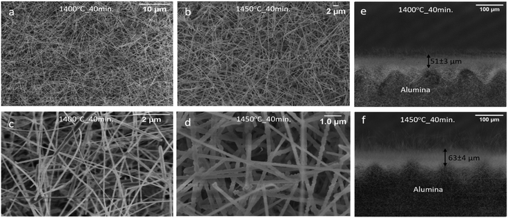 |
| | Fig. 3 FE-SEM images of NiO-GDC nanowires grown at evaporation temperatures of 1400 °C (a, c and e) and 1450 °C (b, d and f). In both cases, nanowires possess dense morphology and their estimated thickness was found to be 51 ± 3 μm (1400 °C) and 63 ± 4 μm (1450 °C). | |
Furthermore, in order to estimate the thicknesses of the nanowire layer, SEM images were acquired by tilting the samples. It should be noted that in the case of randomly oriented nanowires, it is very difficult to find the exact value of thickness as the nanowires were grown in all possible directions such as parallel, perpendicular, etc.Fig. 3e and f present the tilted SEM images of the NiO/GDC nanowires grown at evaporation temperatures of 1400 °C and 1450 °C, respectively. It can be clearly seen that the nanowires were grown even on the sides of the alumina substrates, thus making it more difficult to find the edges. Moreover, some of the islands on the edges of the alumina substrates belong to the laser beam used during the cutting process of the substrate. The estimated thickness values for the whole nanowire layers were found to be 51 ± 3 μm (1400 °C) and 63 ± 4 μm (1450 °C). The higher thickness of nanowires at 1450 °C can be due to the deposition of a higher amount of material (high evaporation rate) as compared to nanowires grown at 1400 °C.
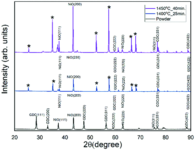
X-Ray diffraction study of NiO-GDC nanowires
Fig. 4 shows the XRD patterns of VLS grown NiO-GDC nanowires along with the pristine NiO-GDC powder. The peaks indexed (*) belong to the alumina substrates and are observed in the case of nanowires only, as deposition was done on alumina substrates.15 In the case of powder, peaks at 2θ = 37.3°, 43.3°, 63° and 75.4° belong to the (111), (200), (220) and (311) hkl planes of NiO respectively8,21 while, for GDC, peaks at 2θ = 28.5°, 33°, 47.4°, 56.2°, 59.1°, 76.7° and 88.2° correspond to the (111), (200), (220), (311), (222), (331) and (422) hkl planes respectively.8
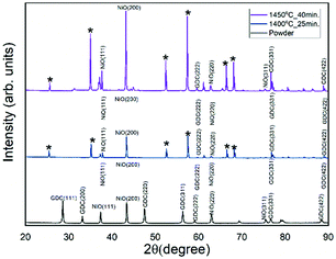 |
| | Fig. 4 XRD spectra of NiO-GDC powder and nanowires grown at evaporation temperatures of 1400 °C and 1450 °C. | |
In the case of nanowires, peaks belonging to GDC i.e. (111), (200), and (220) have not been observed, while most NiO peaks are present. This indicates that NiO-GDC nanowires have more NiO concentration than GDC. This can be due to the difference in the rate of evaporation of NiO and GDC. Furthermore, the nanowires grown at an evaporation temperature of 1450 °C (substrate temperature = 1170 °C) seem to possess higher crystallinity along with a higher concentration of both NiO and GDC (higher intensities of peaks especially NiO (200) and GDC (331)) as compared to the ones grown at 1400 °C. Thus, as GDC possesses ionic conductivity, more ionic contribution to the electrical properties of nanowires grown at 1450 °C can be expected.22 For further investigation of structural and compositional analysis nano-Raman spectroscopy has been performed.
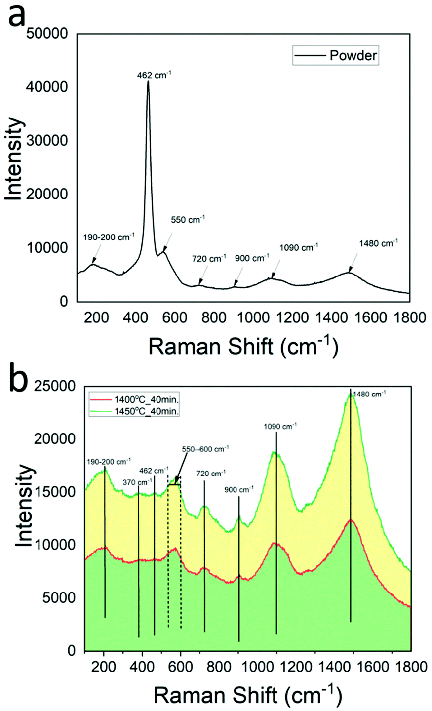
Nano-Raman spectroscopy of NiO-GDC nanowires
To examine the structure, composition, and defects in VLS grown NiO-GDC nanowires, Raman spectroscopy has been performed. Indeed, Raman spectroscopy is a powerful tool that can provide information about the structural defects that may be formed during the growth of nanowires. Furthermore, to eliminate any contribution coming from the alumina substrate, NiO-GDC nanowires were scratched and transferred onto a silicon substrate. For detailed investigation, the Raman spectrum of NiO/GDC powder was also acquired and is shown in Fig. 5a. The high-intensity peak observed at 462 cm−1 is the characteristic band of ceria (F2g symmetry) representing the typical cubic fluorite structure of ceria-based materials. In particular, the F2g symmetric band indicates the symmetrical stretching vibration of Ce–O8 units and involves Ce–O and O–O force constants. Moreover, the intensity of the peak at 462 cm−1 suggests that in the powder the Ce–O bonds exhibit high polarizability with a highly symmetrical CeO2 structure.23 On the other hand, in the case of NiO-GDC nanowires (see Fig. 5b) F2g symmetric bands become broader and extremely low in intensity. This is the indication of asymmetry in the ceria structure and the presence of various defects such as oxygen vacancies. A peak at 550–600 cm−1, which is observed in both powder and nanowires, is the D-band, where D stands for defects. These defects arise from the oxygen vacancies that were created due to the doping of ceria with gadolinium (Gd3+ replaces Ce4+ ions in the ceria lattice). In addition to these defects, another distinctive low intensity peak is observed at 370 cm−1 only in the case of NiO-GDC nanowires (absent in NiO-GDC powder) due to Gd–O vibration, indicating the presence of the cubic Gd2O3 phase.24,25 Thus, the presence of peaks at 462 cm−1 and 370 cm−1 in the NiO-GDC nanowires suggests the simultaneous existence of both C- and F-based microdomains in the hybrid regions of nanowires.26 Furthermore, the existence of the 370 cm−1 peak is also an indication of the fluorite–double fluorite transition which depends upon the doping concentration.27 However, these features are not present in the NiO-GDC powder. Furthermore, many other peaks that are observed in both powder and NiO-GDC nanowires are at ∼200, 720, 900, 1090 and 1480 cm−1. The peaks observed at 1090 and 1480 cm−1 belong to the cubic phase of NiO. Indeed, the peaks at 1090 cm−1 represent the 2LO modes and those at 1490 cm−1 are an indication of two magnon (2 M) scattering while, peaks at 720 cm−1 (2TO (transverse optical)) and 900 cm−1 (TO + LO (longitudinal optical)) occur due to the second order phonon scattering in NiO. Lastly, the peak at ∼190–200 cm−1 arises from the interaction of oxygen vacancies and four nearest neighbor metal atoms.28
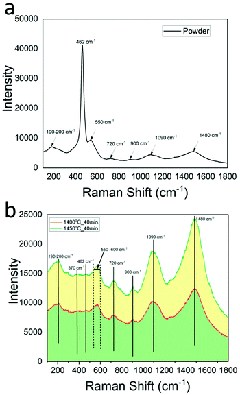 |
| | Fig. 5 (a) Nano-Raman spectrum of NiO-GDC powder indicating the presence of major NiO and GDC peaks. (b) Nano-Raman spectra of NiO-GDC nanowires indicating the formation of a complex structure with defects. | |
Hence, the broadening of the low intensity peak at 462 cm−1 and the coexistence of both C- and F-based microdomains in NiO-GDC nanowires (due to the observation of the peak at 370 cm−1) imply that during the growth of nanowires, reorganization of NiO-GDC particles results in the formation of a more complex structure with defects that diverges from pristine NiO-GDC powder.
Electrical properties of NiO-GDC nanowires
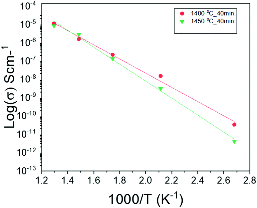
Fig. 6 shows the temperature-dependent electrical conductivity (σ) of NiO-GDC nanowires grown at different evaporation temperatures. The temperature is varied from 100 to 500 °C. In both cases, conductivities of the nanowires increase with the increase of temperature. Indeed, nanowires grown at 1400 °C exhibit slightly higher conductivity as compared to the ones deposited at 1450 °C. Furthermore, the conductivities of nanowires follow the Arrhenius-type activated process, and hence can be expressed with the following equation:29| | 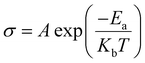 | (2) |
where A is the pre-exponential factor, Ea is the activation energy, Kb = 8.167 × 10⁻⁵ eV K−1 is the Boltzmann constant and T is the absolute temperature. By fitting the equation linearly, the values of activation energies were determined and are shown in Table 1. As can be clearly seen from Table 1, nanowires grown at 1400 °C possess the lowest activation energy. It is well known that the conductivity of the materials is inversely proportional to the activation energy.30 Thus, a low activation energy signifies a better charge carrier transport in the NiO-GDC nanowires, which results in high conductivity. Furthermore, the slightly higher electrical conductivity of nanowires grown at 1400 °C can be associated with the well-defined surface morphology of the nanowires that allows the smooth flow of charge carriers. Another possible reason can be the variation in the concentration of NiO and GDC contents in the nanowires.22 It has been observed that high NiO concentration in the NiO-GDC composite improves the conductivity due to the domination of electronic conduction while high GDC concentration enhances the ionic charge transport, which results in low electrical conductivity of the composite.22 As we have already seen for XRD investigations, the nanowires grown at 1450 °C exhibit a higher concentration of GDC as compared to nanowires deposited at 1400 °C. Hence, the better conductivity of nanowires grown at 1400 °C is also attributed to the lower GDC concentration as compared to other grown nanowires. Furthermore, due to the limitation of our electrical measurement system we were not able to go beyond 500 °C, but an increase in the conductivities of nanowires with temperature is expected at higher temperatures e.g. for intermediate-temperature (500–750 °C) operation of SOFCs. Furthermore, the I–V characteristics of nanowires acquired at 500 °C showed that the nanowires grown at an evaporation temperature of 1400 °C exhibit better conductivity (see the ESI†).
 |
| | Fig. 6 Temperature dependence of electrical conductivity of NiO-GDC nanowires grown at different evaporation temperatures. | |
Table 1 Activation energies of NiO-GDC nanowires grown at different evaporation temperatures. The standard deviation is related to the fitting parameters
| NiO-GDC nanowires |
Growth conditions |
Substrate temperature (°C) |
E
a (eV) |
| Nanowires |
1400 °C_40 min. |
1120 |
0.33 ± 0.18 |
| Nanowires |
1450 °C_40 min. |
1170 |
0.40 ± 0.19 |
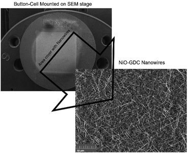
Cell performance and electrochemical impedance spectroscopy
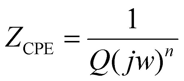
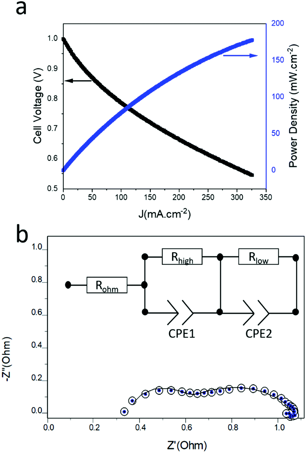
It can be clearly seen from the previous discussion that the nanowires grown at the evaporation temperature of 1400 °C possess superior structural and electrical properties. Thus, these nanowires were selected for the construction of the cell and to investigate cell and electrochemical performance. An electrolyte-supported button cell was fabricated by depositing the NiO-GDC nanowires (1400 °C_40 min) on the commercial single electrode cell-cathode only (see Fig. 7). Fig. 8a shows the plots of cell voltage and power density versus current density at 800 °C. Dry hydrogen and air were used as a fuel and oxidizing agent, respectively. The open-circuit voltage (OPV) was found to be ∼1 V which is similar to the theoretical value of the cell.4 The maximum power density of the cell was found to be ∼178 mW cm−2. We believe the cell performance can be furthermore improved by choosing other cell components such as GDC as an electrolyte (more compatible with the NiO-GDC anode) and other high-performance cathodes. Furthermore, the continuous drop in cell-voltage with respect to current density indicates the presence of typical SOFC losses such as polarization losses etc. in the cell. To investigate it in more detail, electrochemical impedance spectroscopy was performed under the supply of hydrogen fuel and oxidant air. Fig. 8b shows the Nyquist plot (graph between imaginary and real parts of impedance) of the cell indicating the presence of two different semicircles, one is toward the higher frequency region and the other is toward the lower frequency region. These two semicircles were fitted to the equivalent circuit model as shown in the inset of the figure.31,32 Here, Rohm represents the sum of the ohmic resistance offered by anode, cathode and electrolyte. The resistance of the high frequency region (Rhigh) is due to the activation polarization, while mainly results frequency region resistance (Rlow) mainly results from the concentration polarization.31 In fact, the diameter of low frequency semicircle seems to possesses higher values than the diameter of low frequency semicircle, indicating the domination of concentration polarization losses at 800 °C. On the other hand, constant phase elements (CPE1 and CPE2) related to both semicircles in the Nyquist plot represent the capacitance of non-ideal and non-homogeneous systems.33,34 The expression for such an impedance is given by| |  | (3) |
where ω is the angular frequency of the AC signal, j is the imaginary unit, and the value of n lies in the range −1 to 1. The different parameter values obtained after fitting are shown in Table 2. In particular, the area specific ohmic resistance of the cell was found to be 0.44 Ohm cm2. While the total resistance of the cell (Rtot = Rohm + Rhigh + Rlow) was found to be 1.29 Ohm cm2.
 |
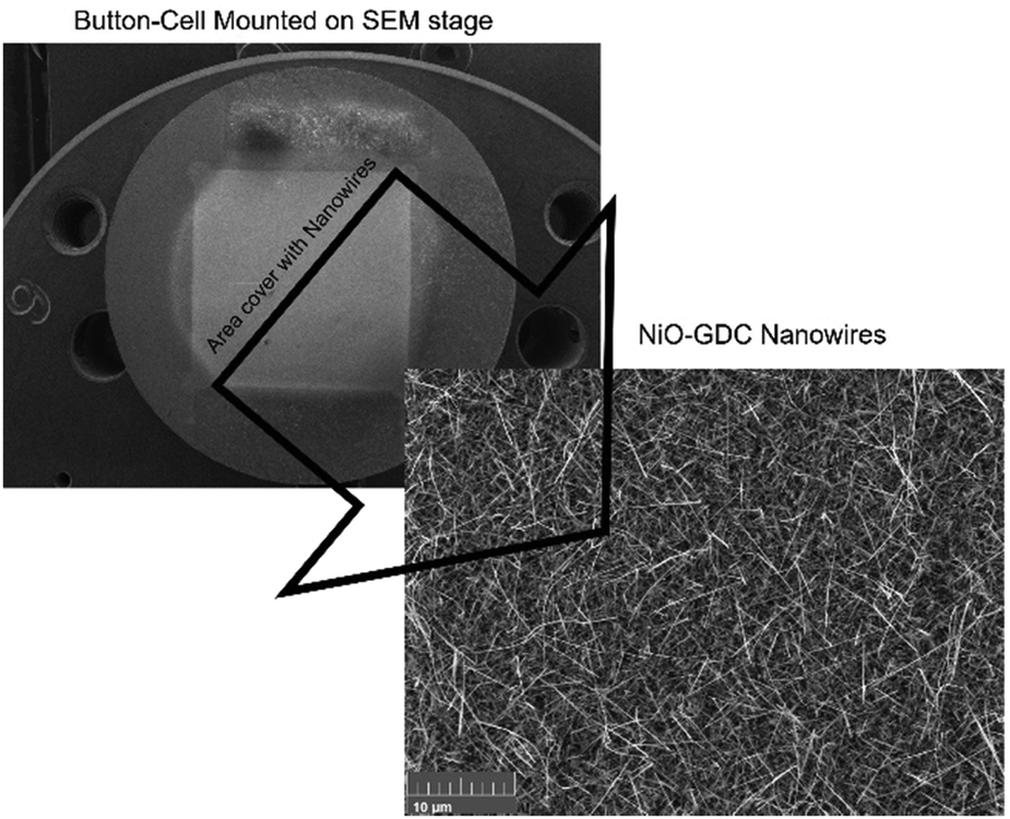
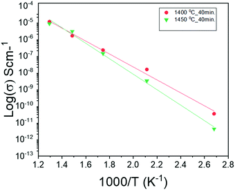
| | Fig. 7 Button-cell mounted on a SEM stage along with the SEM image of NiO-GDC nanowires. The same morphology of nanowires was achieved as shown in Fig. 3. | |
 |
| | Fig. 8 (a) Voltage and power density vs. current density at 800 °C of the button cell fabricated using NiO-GDC nanowires grown at an evaporation temperature of 1400 °C. (b) Nyquist plot of the button cell at 800 °C indicating the presence of two semicircles. The equivalent circuit for the cell is shown in the inset of the Nyquist plot. | |
Table 2 The EIS parameters obtained after fitting the Nyquist plot to the equivalent circuit presented in Fig. 8b
| Fit parameters |
Values |
|
R
ohm (ohm cm2) |
0.44 |
|
R
high (ohm cm2) |
0.27 |
|
R
low (ohm cm2) |
0.58 |
| CPE1 |
1.3 × 10⁻⁵ |
| CPE2 |
6.9 × 10⁻³ |
|
n1 |
1 |
|
n2 |
∼0.7 |
Conclusions
In conclusion, novel NiO-GDC nanowires were successfully synthesized using the VLS mechanism under different experimental conditions for their potential application as an anode of small-scale SOFCs. These nanowires exhibit dense morphology with varied diameters. Indeed, the observed higher diameter of nanowires grown at 1450 °C evaporation temperature (substrate temperature: 1170 °C) is found to be associated with the merging of Au-nanoparticles. Furthermore, the observation of an additional Raman peak at 370 cm−1 and the broadening of the low intensity peak at 462 cm−1 in the case of nanowires suggest that during the growth of nanowires reorganization of NiO-GDC particles results in the formation of a more complex structure, with defects that diverge from the pristine NiO-GDC powder. On the other hand, the high temperature dependence of the electrical conductivity and lowest activation energy of NiO-GDC nanowires grown at 1400 °C indicate an improved charge-carrier transport as compared to nanowires grown at 1450 °C. Furthermore, the electrolyte supported button cell fabricated using NiO-GDC nanowires grown at 1400 °C exhibits a maximum power density of ∼178 mW cm−2 at 800 °C. EIS reveals the domination of concentration losses in the cell performance, and the total resistance (Rtot) of the cell was found to be 1.29 Ohm cm2. Hence, based on our preliminary investigations, NiO-DGC nanowires grown at the evaporation temperature of 1400 °C have the potential to be used as an anode of SOFCs especially for small-scale applications.
Author contributions
Mandeep Singh: performed the synthesis, optimization, characterization, and data analysis. The author also wrote the manuscript. Dario Zappa: was involved in all the characterization and edited the manuscript. Elisabetta Comini: supervised the work and edited the manuscript. The idea was conceived with collective discussion among all the authors.
Conflicts of interest
There are no conflicts to declare.
Acknowledgements
Dr Mandeep Singh acknowledges the project BioMassHUB (ID: 1165247), “POR-FESR 2014–2020/innovazione e competitivita” funded by EU and Regione Lombardia.
References
- A. Mohapatra and S. Tripathy, IOP Conf. Ser.: Mater. Sci. Eng., 2018, 377, 12135 CrossRef.
- O. Z. Sharaf and M. F. Orhan, Renewable Sustainable Energy Rev., 2014, 32, 810–853 CrossRef CAS.
- I. Sreedhar, B. Agarwal, P. Goyal and S. A. Singh, J. Electroanal. Chem., 2019, 848, 113315 CrossRef CAS.
- M. Singh, D. Zappa and E. Comini, Int. J. Hydrogen Energy, 2021, 46, 27643–27674 CrossRef CAS.
- N. Mahato, A. Banerjee, A. Gupta, S. Omar and K. Balani, Prog. Mater. Sci., 2015, 72, 141–337 CrossRef CAS.
- S. C. Singhal, WIREs Energy Environ., 2014, 3, 179–194 CrossRef CAS.
- E. Traversa, Electrochem. Soc. Interface, 2009, 18, 49–52 CrossRef CAS.
- M. G. Chourashiya, S. R. Bhardwaj and L. D. Jadhav, J. Solid State Electrochem., 2010, 14, 1869–1875 CrossRef CAS.
- F. J. Garcia-Garcia, F. Yubero, A. R. González-Elipe and R. M. Lambert, Int. J. Hydrogen Energy, 2018, 43, 885–893 CrossRef CAS.
- B. Timurkutluk, C. Timurkutluk, M. D. Mat and Y. Kaplan, J. Power Sources, 2011, 196, 9361–9364 CrossRef CAS.
- F. J. Garcia-Garcia, A. M. Beltrán, F. Yubero, A. R. González-Elipe and R. M. Lambert, J. Power Sources, 2017, 363, 251–259 CrossRef CAS.
- Q. Zhang, E. Uchaker, S. L. Candelaria and G. Cao, Chem. Soc. Rev., 2013, 42, 3127–3171 RSC.
- N. Kaur, M. Singh and E. Comini, Langmuir, 2020, 36, 6326–6344 CrossRef CAS PubMed.
- E. Comini, Mater. Today Adv., 2020, 7, 100099 CrossRef.
- N. Kaur, E. Comini, D. Zappa, N. Poli and G. Sberveglieri, Nanotechnology, 2016, 27, 205701 CrossRef CAS PubMed.
- M. Singh, N. Kaur, G. Drera, A. Casotto, L. S. Ermenegildo and E. Comini, Adv. Funct. Mater., 2020, 2003217 CrossRef CAS.
- N. Kaur, E. Comini, D. Zappa, N. Poli and G. Sberveglieri, Nanotechnology, 2016, 27, 205701 CrossRef CAS PubMed.
- E. Comini, C. Baratto, G. Faglia, M. Ferroni, A. Vomiero and G. Sberveglieri, Prog. Mater. Sci., 2009, 54, 1–67 CrossRef CAS.
- M. R. Khanlary, S. Alijarahi and A. Reyhani, J. Theor. Appl. Phys., 2018, 12, 121–126 CrossRef.
- X. Fang, T. Zhai, U. K. Gautam, L. Li, L. Wu, Y. Bando and D. Golberg, Prog. Mater. Sci., 2011, 56, 175–287 CrossRef CAS.
- S.-Y. Park, C. W. Na, J. H. Ahn, R.-H. Song and J.-H. Lee, J. Aust. Ceram. Soc., 2014, 2, 339–346 CrossRef.
- J. Durango-Petro, C. Salvo, J. Usuba, G. Abarzua, F. Sanhueza and R. V. Mangalaraja, Materials, 2021, 14, 3437 CrossRef CAS PubMed.
- S. Loridant, Catal. Today, 2021, 373, 98–111 CrossRef CAS.
- R. Schmitt, A. Nenning, O. Kraynis, R. Korobko, A. I. Frenkel, I. Lubomirsky, S. M. Haile and J. L. M. Rupp, Chem. Soc. Rev., 2020, 49, 554–592 RSC.
- C. Artini, M. Pani, M. M. Carnasciali, M. T. Buscaglia, J. R. Plaisier and G. A. Costa, Inorg. Chem., 2015, 54, 4126–4137 CrossRef CAS PubMed.
- C. Artini, M. Pani, M. M. Carnasciali, M. T. Buscaglia, J. R. Plaisier and G. A. Costa, Inorg. Chem., 2015, 54, 4126–4137 CrossRef CAS PubMed.
- R. Schmitt, A. Nenning, O. Kraynis, R. Korobko, A. I. Frenkel, I. Lubomirsky, S. M. Haile and J. L. M. Rupp, Chem. Soc. Rev., 2020, 49, 554–592 RSC.
- M. Coduri, M. Scavini, M. Pani, M. M. Carnasciali, H. Klein and C. Artini, Phys. Chem. Chem. Phys., 2017, 19, 11612–11630 RSC.
- A. K. Soman, P. Kuppusami and A. M. Rabel, Nano Hybrids, 2017, 17, 224–236 Search PubMed.
- M. Sharma and S. Yashonath, J. Chem. Phys., 2008, 129, 144103 CrossRef PubMed.
- N. Shikazono, Y. Sakamoto, Y. Yamaguchi and N. Kasagi, J. Power Sources, 2009, 193, 530–540 CrossRef CAS.
- D. Panthi and A. Tsutsumi, Sci. Rep., 2014, 4, 5754 CrossRef CAS PubMed.
-
E. Barsoukov and J. R. Macdonald, Impedance Spectroscopy, 2005 Search PubMed.
- M. Singh, K. Manoli, A. Tiwari, T. Ligonzo, C. Di Franco, N. Cioffi, G. Palazzo, G. Scamarcio and L. Torsi, J. Mater. Chem. C, 2017, 5, 3509–3518 RSC.
|
| This journal is © The Royal Society of Chemistry 2022 |
Click here to see how this site uses Cookies. View our privacy policy here. 
 Open Access Article
 This Open Access Article is licensed under a
  *,
Dario
Zappa
*,
Dario
Zappa