
 Open Access Article
 This Open Access Article is licensed under a
 Creative Commons Attribution 3.0 Unported Licence
Photovoltaic properties of hybrid c-Si/ZnO nanorod solar cells
M.
Mohammadnezhad
a,
B.
Aïssa
 *bc,
C.
Harnagea
a,
A.
Bentouaf
de,
E.
Haddad
b and
F.
Rosei
*a
*bc,
C.
Harnagea
a,
A.
Bentouaf
de,
E.
Haddad
b and
F.
Rosei
*a
aInstitut National de la Recherche Scientifique, Centre Énergie, Matériaux et Télécommunications, 1650 Boul. Lionel Boulet, J3X 1P7 Varennes (QC), Canada. E-mail: federico.rosei@inrs.ca
bMPB Communications Inc., Department of Smart Materials and Sensors for Space Mission, 151, Hymus Boulevard, Pointe Claire, Montreal, Canada. E-mail: baissa@hbku.edu.qa
cQatar Environment and Energy Research Institute (QEERI), Hamad Bin Khalifa University (HBKU), Qatar Foundation, P. O. Box 5825, Doha, Qatar
dFaculty of Technology, University of Dr Moulay Tahar, Saida, 20000, Algeria
eLaboratory of Physical Chemistry of Advanced Materials, University of Djillali Liabes, BP 89, Sidi-Bel-Abbes, 22000, Algeria
First published on 26th May 2022
Abstract
We report on the hydrothermal synthesis of high quality polycrystalline zinc oxide nanorod arrays grown on indium tin oxide substrates. We observe a clear effect of the nucleation and growth rates on the morphology and orientation of the nanorod arrays, with a predominance of the polycrystalline hexagonal wurtzite structure and preferential c-axis orientation. In addition, we studied the effect of the growth orientation and morphology of the ZnO nanorod arrays on light absorption. The changes in crystalline structure and defects are attributed to kinetic effects driven by temperature. Finally, using PC1D software, we describe the charge transport and photovoltaic properties of simulated hybrid c-Si solar cells by considering the lengths of the ZnO NRs and the reflectance values. The 1.1 μm average length of the ZnO NRs is found to be the optimum value for achieving the highest power conversion efficiency of ∼15.48%. The simulation study for the vertically arranged ZnO NRs anti-reflection layers shows that the low-temperature grown ZnO NRs on the c-Si solar cells is promising for the realization of low-cost and efficient hybrid solar cells.
Introduction
Nanostructured materials are widely investigated due to their surprising properties, which are often size tunable. More broadly, their mechanical, electrical, optical and physico-chemical properties depend on the structure, composition and size of a nanoscale system.1–8 The shape of nanostructured materials can be simply classified based on the dimensionality: zero-dimensional (0D), one dimensional (1D), two-dimensional (2D) and three-dimensional (3D).4During the last two decades, low dimensional nanostructures such as 0D quantum dots (QDs) and 1D nanorods (NRs) and nanowires (NWs) have stimulated a growing interest because of their importance for understanding fundamental phenomena and also for their wide range of potential applications.4,9–11 They can efficiently transport charge due to their anisotropy and other structural features such as decreased grain boundaries and surface defects.9,11,12 In addition, NRs exhibit high-performances in different applications due to their high surface-to-volume ratio and unusual physical properties.8,9,12–14
Metal oxide semiconductors have also been intensively investigated because of their properties, including excellent charge transport, toughness, strain tolerance and thin film processing, compared with other classes of semiconductors.15–17 Among various metal oxides, zinc oxide (ZnO) is being studied extensively for a wide variety of applications such as photocatalysis, photovoltaics and electronic devices owing to its wide bandgap, large exciton binding energy, excellent chemical and thermal stability, as well as electrical and optical properties.10,12,13,18,19 Various techniques have been used for growing ZnO NRs in order to control their shape to optimize their physical properties, which include pulsed laser deposition,20 thermal evaporation,21 vapor–liquid–solid growth 9 and chemical vapor deposition.22 However, these methods require strict process control, accurate gas concentration and rigid gas flow and are energy intensive. On the other hand, hydrothermal synthesis is a simple, low cost and energy-efficient method to obtain ZnO NRs.23,24 In this method, a seed layer is used to control the morphology and growth direction of NRs.25,26 Vayssieres and coworkers originally reported an approach based on low temperature aqueous chemistry for the growth of ordered NRs and NWs arrays of ZnO8 which is also applicable to other metal oxides, including Fe2O3 and SnO2. However, the hydrothermal growth of ZnO NRs with controlled structural and morphological properties is usually challenging and there is a lack of general theoretical guidance in experimental approaches. Demes et al.27 reported the effect of the substrate temperature and chemical concentration on the growth mechanism of high aspect ratio ZnO NWs using hydrothermal synthesis. Kumaresan and coworkers28 investigated the effect of UV irradiation and solution pH on the structural, optical and morphological properties of synthesized ZnO NWs. Kwon et al.29 described the hydrothermal growth mechanism of ZnO NRs, while many other groups30–32 illustrated the effect of the ZnO seed-layer density on the size distribution of the grown NRs. The effect of the ZnO seed-layer thicknesses on the quality of the synthesized ZnO NWs has been investigated in depth.33–36 Other studies highlighted the effects of Al-doped concentrations and synthesis parameters on the microstructural, electrical and optical properties of ZnO thin films.37–39
While numerous studies emphasized the influence of the synthesis parameters on the morphology of ZnO nanostructures, the effect of temperature on the structure and properties of ZnO NRs in hydrothermal synthesis is not yet fully understood. The aim of this work is thus to describe the effect of the nucleation and growth rates on the morphology and orientation of ZnO rod arrays and to determine their structure/property relationships. More specifically, the focus is put on the effect of the growth orientation and morphology of the ZnO nanorod arrays on light absorption, and the changes in the crystalline structure and defects. We compare thoroughly the properties of ZnO nanorod arrays grown at various temperatures, including their nano/microstructure, surface morphology, crystallinity, and electrical and optical properties. Furthermore, using the length and reflectance of a ZnO NRs anti-reflection (AR) layer, the photovoltaic parameters are extracted through a simulation study via PC1D software.
Experimental
Materials and method
A schematic diagram of the formation mechanism of ZnO rods based on the theory of crystal nucleation and growth is shown in Fig. 1.8 The most widely used substrate for applications in photovoltaics is indium tin oxide (ITO), hence it is our choice to assess the potential performance in solar technologies. ZnO thin films were deposited on ITO substrates by spin coating, as described in detail below. Subsequently, hydrothermal synthesis was used to grow ZnO nanostructures.8,24 Prior to deposition, ITO glass substrates were ultrasonically cleaned in acetone, methanol and deionized water and then dried in flowing nitrogen gas.22,29 The seed layer was prepared using a mixed solution of 0.5 M zinc acetate (Sigma Aldrich) in ethanol solvent.37 Thin films of ZnO were prepared onto pre-cleaned ITO substrates at a rotation speed of 3000 rpm for 30 seconds in ambient conditions, followed by drying at 150 °C for 10 minutes in air to evaporate the solvent. This process was repeated five times to develop a uniform film. ZnO NRs were then grown on the ZnO ultrathin (approximate 40 nm in thickness) seed-layer via hydrothermal synthesis.25 The hydrothermal reaction was carried out at different temperatures ranging from 70 to 115 °C, for 4 hours, in Teflon-lined stainless steel autoclaves. The hydrothermal reaction solution for NR growth was prepared by dissolving (0.5 M) equimolar zinc nitrate (Zn(NO3)2) and hexamethylenetetramine (HMT) (Sigma Aldrich) in deionised water. After the reaction, the autoclave was cooled down to room temperature, and the resulting samples were taken out, thoroughly rinsed with ethanol and deionized water and dried in air for characterization.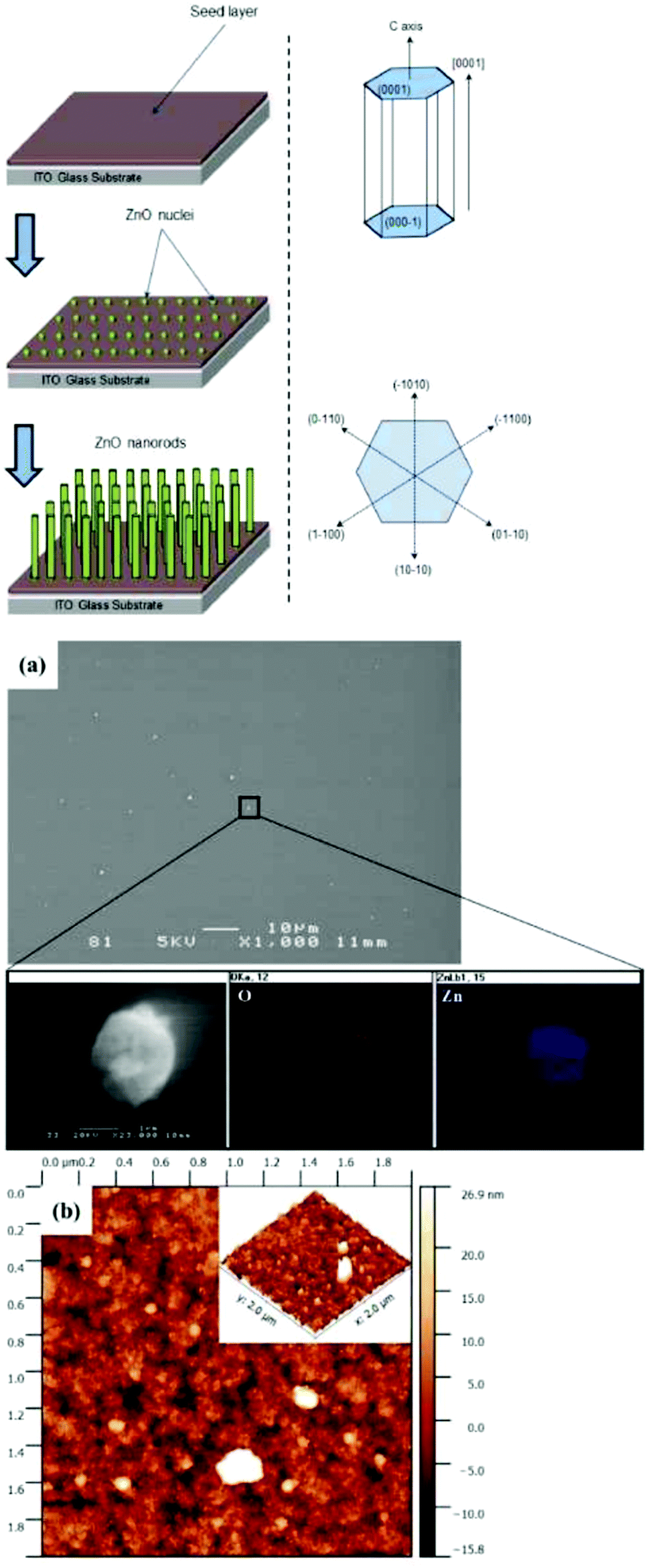 | ||
| Fig. 1 (Upper panel) Schematic illustration of the crystal nucleation and growth of the ZnO NRs and crystal structure of wurtzite ZnO structure. (a) Typical top view FE-SEM micrograph of the as-deposited seed layer on an ITO-coated glass substrate and (b) tapping mode AFM image of the surface morphology of the seed layer. | ||
Measurements
Sample morphologies were imaged by field emission scanning electron microscopy (FE-SEM, JEOL JSM-6300 F) and transmission electron microscopy (TEM) (JEOL JEM-2100 F FEG-TEM equipped with a selected area electron diffractometer (SAED)). Surface morphologies were examined by atomic force microscopy (AFM). We used an Enviroscope AFM (Digital Instruments) operated in tapping mode at room temperature in ambient air, and a JEOL 4500 UHV AFM/STM for higher resolution images. Raman spectroscopy measurements were acquired with 514.5 nm (2.41 eV) laser radiation of an Ar+ laser focused onto the sample with a spot diameter of 1 μm (micro Raman spectroscopy, Renishaw Imaging Microscope Wire TM), equipped with a CCD detector. To prevent photo-induced degradation, Raman scattering was excited with a power not exceeding 1 mW. Raman spectra were acquired in a backscattering geometry, at room temperature in the 150–800 cm−1 region. Structural studies were performed using X-ray diffraction (XRD, Bruker D8-40 kV/40 Ma generator advanced diffractometer) using a Cu Kα radiation source (λ = 1.54 Å). The typical settings of the XRD instrument were as follows: 40 kV and 30 mA for the X-ray source and scanning angle (2θ) range 20–80°. The absorbance spectra of the produced films were measured using a UV-Vis spectrometer (Jenway-67 Series spectrophotometer). Photoluminescence was performed on as-grown and thermally annealed (at 450 °C, for 1 hour, under air and under inert Ar atmosphere) samples using a 325 nm excitation from a He–Cd laser. The spectra were recorded using the fiber optic spectrometer PDA-512-USB, Control Development Inc. The numerical modeling software PC1D has been used to simulate the PV properties of hybrid c-Si/ZnO NWs solar cells.40 Several key parameters, including active area, the thickness of absorbing material, bandgap, and reflectance, were used to perform the simulation for the photovoltaic parameters of the solar cells. In this work, the PC1D simulation was performed using the NR lengths and the average reflectance of the ZnO NRs antireflective (AR) layer over the textured c-Si wafer, and the simulated performance and charge transport properties were based on a vertically arranged ZnO NRs AR layer scheme. The selected parameters for this simulation are summarized in Table 1.| Parameters | Value |
|---|---|
| Device area | 4 × 4 cm2 |
| Front surface texture depth | 0–5 μm |
| Front reflectance | 2–4% |
| Thickness of Si solar cell | 120 μm |
| Dielectric constant | 11.9 |
| Energy bandgap | 1.124 eV |
| Background doping P-type | 1.513 × 1016 cm−3 |
| First front diffusion N-type | 2.87 × 1020 cm−3 |
| Refractive index | 3.58 |
| Excitation mode | Transient |
| Temperature | 25 °C |
| Other parameters | Internal model of PC1D |
| Primary light source | AM 1.5D spectrum |
| Bulk recombination | 10 μs |
| Constant intensity | 100 mW cm−2 |
| Minimum average reflectance | 9.5% |
Results and discussion
The morphology of the seed layer, including thickness, grain size and film uniformity strongly influences the structural properties of the subsequently grown ZnO NRs.38Fig. 1a shows representative FE-SEM and AFM micrographs of the seed layer that was deposited onto the ITO-coated glass substrate.ZnO thin films with uniform and flat surface morphology were obtained using the process conditions described in the Experimental section. Some ZnO seed particles were found on the surface, due to the agglomeration of individual nanoparticles. High surface energy and thermodynamic instability have been reported as two possible reasons for the agglomeration of nanoparticles.30 The chemical composition of ZnO particles was confirmed by EDS spectra. Fig. 1b displays a typical AFM image of a relatively dense and homogeneous ZnO seed layer, which provides an array of nucleation sites for the growth of ZnO rods. Fig. 2 displays top view FE-SEM images of the grown ZnO film at a reaction temperature of 70 °C and a growth time of 4 hours. This growth temperature is found to be insufficient for complete formation of ZnO rods, since the coverage is not uniform and many agglomerated islands are observed on the surface (bright zones in Fig. 2a). Higher magnification SEM imaging (Fig. 2b) shows that these areas consist of very thin nanorods (∼70 nm in diameter).
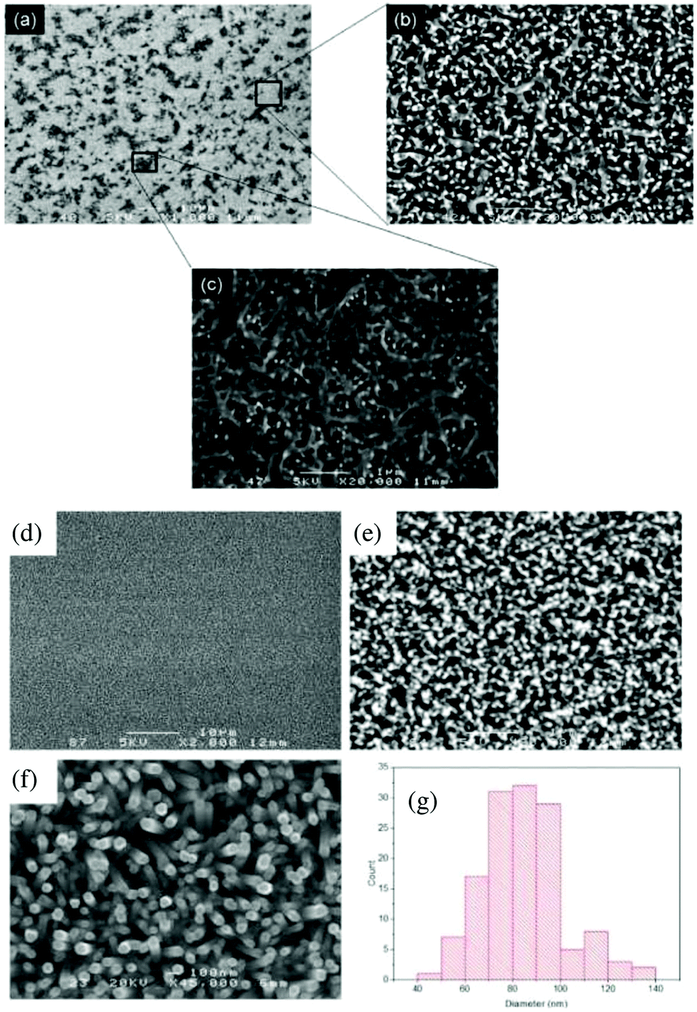 | ||
| Fig. 2 (a) Typical FE-SEM micrographs of ZnO NRs synthesized at 70 °C, (b) is a close-up view of the bright zones in (a) showing grown ZnO rods, while (c) is the dark location magnification. (d) Representative FE-SEM micrographs of ZnO synthesized at 85 °C, (b and c) are higher magnification images and (e) shows histograms of the ZnO NRs size distributions. | ||
Crystal growth is known to occur in two main phases, nucleation and growth. First, zinc ions adsorb on the seed surface, followed by their dissolution to initiate the nucleation and growth processes, depending on the reaction temperature. During the hydrothermal reaction, the active zinc atoms located at the surface of the seed film layer first react with water and oxygen molecules, leading to an increase in the concentration of zinc ions. Subsequently, the zinc ions transform into ZnO and form particles through the in situ dehydration reaction under hydrothermal conditions, thus providing feedstock for the growth of ZnO NR arrays.30–39 From a kinetic point of view, by selecting a suitable reaction temperature and appropriate reaction time, the ZnO seeds formed on the substrate gradually grow into NRs in the c-axis direction following the intrinsic crystallographic structure.37,38
Fig. 2d shows FE-SEM micrographs of a uniform and dense array of ZnO NRs (70–100 nm in diameter) grown at 85 °C along the c-axis (002), whereas Fig. 2e displays ZnO NRs grown at 100 °C, yielding structures with a different morphology. When the reaction temperature is increased from 85 to 100 °C, the average diameter of the NRs increases from about 100 to 400 nm, respectively. Fig. 2f indicates that hexagonal microrods grow directly onto polyhedral particles with an average diameter of about 80 nm (histogram in Fig. 2e) and a length of around 1.1 μm. The dendrite structures with a main trunk and several side branches develop as the reaction temperature increases. This mechanism can be described as follows: at a higher temperature, ZnO particles at the seed layer agglomerate to form a hexagonal planar nucleus. The thermodynamically stable crystal structure of ZnO is known to be the wurtzite phase (hexagonal crystal system), which is an ionic and polar close-packed structure of oxygen and zinc atoms. Zn atoms are tetrahedrally coordinated with four oxygen atoms, so that one face of the hexagonal sheet is Zn rich and forms (0001) planes. The ZnO crystals are polar in nature, as a result of Zn (0001) and oxygen (000−1) rich surfaces with positive and negative charges, respectively.41 The negative surface (000−1) is less reactive compared to the positive one (0001), so a Zn rich positive surface attracts opposite ions. In addition, the growth rate of planes in the ZnO crystals follows the sequence (0001) > (1011) > (1010), which means that the polar (0001) is the fastest one as compared to other facets. Hence, zinc oxide structures are grown preferentially along the [0001] direction with six (1010) facets.42–44
By increasing the reaction temperature to 115 °C, hexagonal zinc oxide symmetric surface structures with various orientations were obtained, as shown in Fig. 3a–e. This evolution of the morphology suggests that ZnO NRs serve as an intermediate phase for these newly obtained structures. In our experiments, at lower temperatures (∼70 °C), large sized crystals were the only ones formed because they are more stable from a thermodynamic point of view.45–47 Pyramid-shaped ZnO NRs were obtained upon increasing the temperature, starting from 85 °C. Indeed, by increasing the reaction temperature, the mobility and diffusion length of the ions increase accordingly and reach the nucleation sites leading to the formation of ZnO NRs. Fig. 4 shows the patterns of the XRD diffraction intensity of ZnO products obtained at different reaction temperatures. The diffraction peaks arising from the ZnO rod arrays are well indexed to the standard diffraction pattern of wurtzite hexagonal structured ZnO, with a = 3.251 Å and c = 5.208 Å (JCPDS 36-1451).47 Except for the peaks originating from the ITO substrate, no other impurity peaks were detected, which is a clear indication that the prepared films are made of pure polycrystalline ZnO. XRD results also demonstrate that the hydrothermal temperature reaction directly determines both the orientation and morphology of the ZnO structure as the patterns change significantly when the temperature reaction varies.
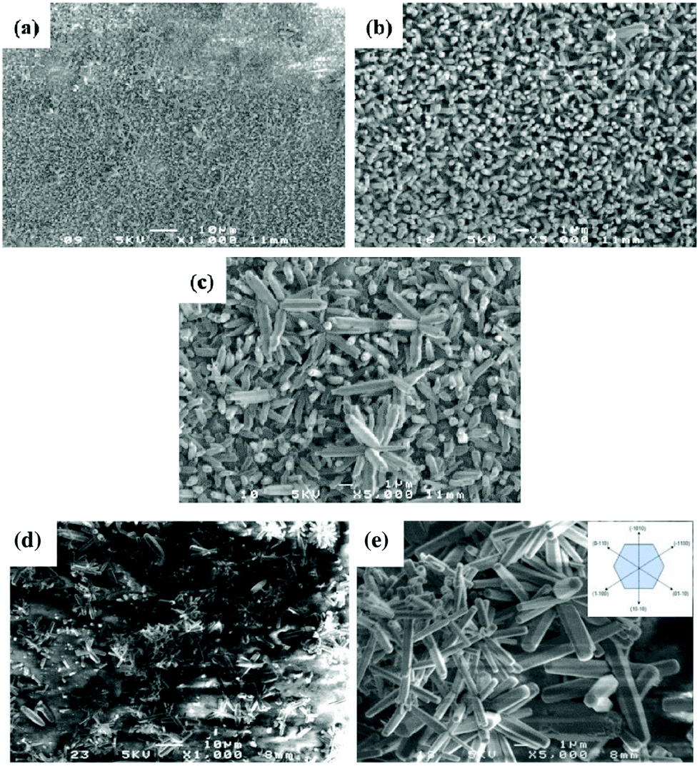 | ||
| Fig. 3 (a) Representative FE-SEM micrographs of ZnO synthesized at 100 °C. (b) and (c) are close-up views of the image in (a) taken at different locations. (d) Typical FE-SEM micrographs of ZnO synthesized at 115 °C; (e) is a close-up view of (d) showing clearly the ZnO NRs with different orientations. The six (1010) facets family of the ZnO hexagonal crystal system is shown in the inset. | ||
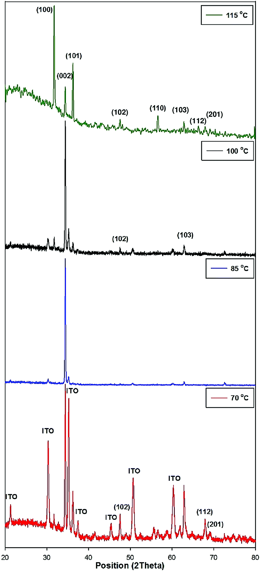 | ||
| Fig. 4 XRD patterns of ZnO NR arrays synthesized at different temperatures, for 4 h. | ||
At 70 °C, both ZnO and ITO diffraction peaks appear, and the (002), (100), (101), (102), (201), (112), and (103) peaks, which indicate a polycrystalline nature with random orientations, are observed. However, the intensity of the ITO substrate diffraction peaks declines and nearly disappears with respect to the increasing reaction temperature. This reduction trend might be due to NR formation at a higher temperature.44,48–50 As the hydrothermal temperature increases to 85 °C, the intensity of the (002) peak increases accordingly (preferential orientation of ZnO NR arrays, perpendicular to the substrate's orientation).39
At a higher temperature (115 °C), well defined diffraction peaks are observed, confirming the crystalline nature of the ZnO NRs. All the diffraction peaks correspond to the hexagonal wurtzite structure of ZnO. The nature of the diffraction peaks is an indication of the nanocrystalline nature of the NRs. The characteristic hexagonal zinc oxide peaks (100), (002), (101), (110) (102), (103), (112) and (201) are all present in the X-ray diffractogram with no extra peaks ruling out the possibility of impurities. The presence of nanocrystallites is expected to increase the surface area and thus results in improved current density. The intensity of the (100) diffraction peak is shown to particularly increase at this temperature, thus indicating the new crystalline preferential orientation. Shi et al.38 demonstrated that (100) textured films are suitable for piezoelectric and acousto-optical device applications because (001) oriented films correspond to a larger dielectric constant and loss values. In addition, by increasing the temperature from 85 to 115 °C, the intensity of the (101) peaks increases gradually, while that of the (002) peak decreases.
Alshanableh and coworkers49 suggested that in the ZnO hexagonal crystal the (101) is an effective plane for twinning orientation and dislocation process during crystal growth, due to a limited slip system in the hexagonal structure. Two obvious strategies for these changes are the attractive force near the stacking fault boundary and the repulsive force between the partial dislocations. Previous studies suggested that during the phase transformation of nanomaterials, two mechanical defects, namely deformation twinning and crystallographic slip could develop new physical properties, such as dielectricity and mechanical strength.37,38
The phase and morphology of the ZnO NRs were further characterized by TEM and selected area electron diffraction (SAED). Fig. 5 illustrates TEM micrographs of ZnO NRs grown at 85 °C. Fig. 5a shows hexagonal ZnO NRs with a diameter of about 100 nm. The high-resolution HRTEM image displayed in Fig. 5b further confirms that the nanorod has a single crystal structure, and reveals a lattice spacing of 0.26 nm, corresponding to the distance between the (002) planes, indicating thereby that the nanorods grow along the [0001] crystallographic direction, in agreement with XRD analysis. The distance between the diffraction spots on the corresponding Fast Fourier transform (FFT) pattern is also consistent with HRTEM analysis. The average crystallite size (D) of the ZnO films composed of rods was estimated using the well-known Debye-Scherrer relation:
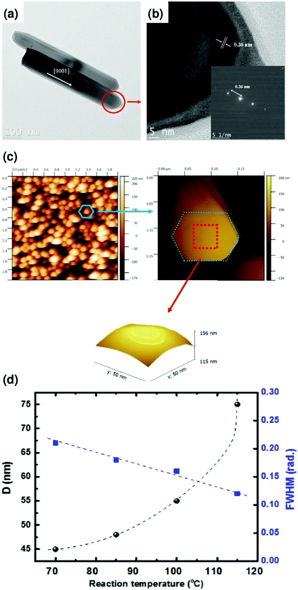 | ||
| Fig. 5 (a) TEM image of two ZnO NRs. (b) HRTEM image taken from the marked area, the inset shows the FFT pattern of the HRTEM image. High resolution images of TEM and FFT patterns of the NRs showing a lattice spacing of 0.26 nm. (d) Representative AFM images of the surface morphology of ZnO NRs grown at 85 °C. (e) The variation of crystallite size (D) and the corresponding FWHM with respect to the reaction temperatures. The dashed-lines are for eye-guiding purposes. | ||
Fig. 5b shows the FWHM and average grain size of the (002) diffraction peak in the ZnO thin films composed of rods as a function of reaction temperature. When the hydrothermal temperature increases from 70 °C, the FWHM tends to decrease, indicating an improvement in the crystalline quality of the grown ZnO.22,51 Synthesis at higher temperature could increase the nucleation and growth rates, which tend to favor defect elimination and improve the crystallinity during the growth as reported by Liang and coworkers.22 The average crystallite size was also found to increase with respect to the reaction temperature. This could be explained in terms of the two following factors: (i) the thermal process induces diffusion and then coalescence of small grains, and (ii) reduction of the crystallographic defects such as dislocations, interstitials and vacancies when the reaction temperature increases.12,18
Fig. 5c displays an AFM image of ZnO structures grown at 85 °C. In agreement with the XRD (Fig. 4) and FE-SEM (Fig. 3) measurements, this sample shows homogenous vertical growth of ZnO NRs, in which no cracks are noticed. The high-resolution image (50 nm scan size) shows that the (0001) surface perpendicular to the growth direction is curved (consistent with the TEM images in Fig. 5), further confirming the nucleation-based growth mechanism of the rods. On the other hand, AFM characterisation of samples grown at a higher temperature (Fig. 3) was not possible because of the increasing height of the rods.
The effects of the hydrothermal reaction temperature on the optical properties of the grown ZnO thin films composed of rods were also investigated by means of UV-Vis absorbance spectroscopy, as shown in Fig. 6a. Regardless of the growth temperature, the near band-edge (NBE) absorption located at 270–400 nm was systematically observed, as a consequence of the electronic transitions from the valence to the conduction band of ZnO.49 The increase of the NBE with respect to the reaction temperature was not linear, and the samples prepared at 85 °C showed up to 56% higher UV absorption than those prepared at 100 °C, in the region between 290 and 370 nm. This is most probably due to the difference in their internal light scattering and respective surface exposed to light irradiation.
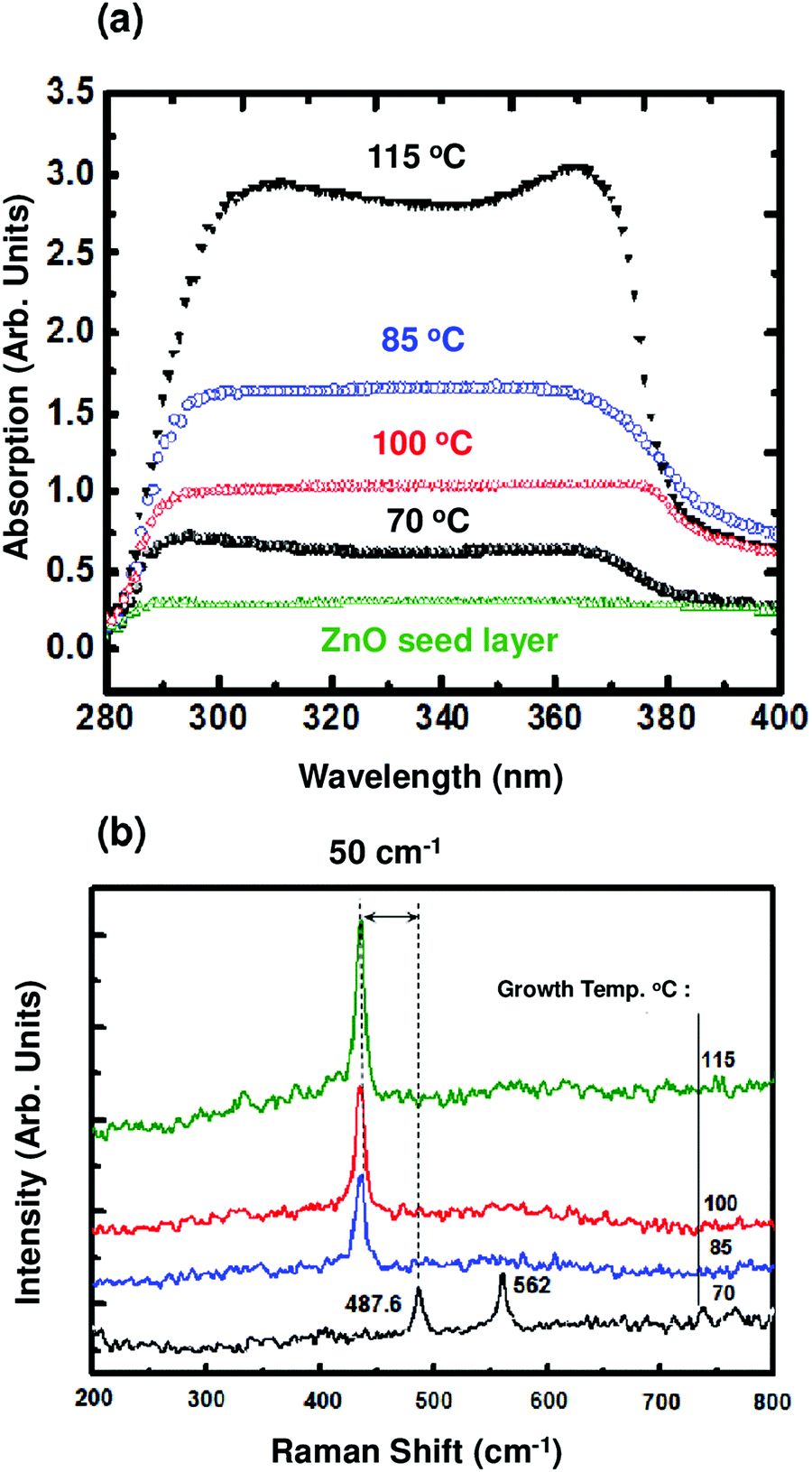 | ||
| Fig. 6 (a) UV absorption spectra of ZnO NRs arrays grown at different temperatures. (b) Raman spectra of the ZnO NR arrays synthesized at different temperatures. | ||
Finally, to further study the vibrational properties of the grown ZnO samples and analyse the changes in microstructure and inner defects, we acquired Raman spectra from the samples grown at different reaction temperatures (displayed in Fig. 6b). The ZnO wurtzite hexagonal phase belongs to the space group C6v4 and has two formula units per primitive cell where all atoms occupy the sites of symmetry C3v. Based on the group theory analysis of the ZnO structure52–56 among eight sets (2A1 + 2B1 + 2E1 + 2E2) of optical modes, the A1 and E1 modes are both Raman and infrared active, two E2 modes are only Raman active and two B1 modes are neither Raman nor infrared active (silent) modes. The A1 and E1 modes are polar in nature and therefore split into two transverse optical (TO) and longitudinal optical (LO) phonons. Nonpolar phonon modes with symmetry E2 have two frequencies, namely E2 high and E2 low, which are associated with oxygen atoms and the Zn sublattice, respectively. We observed two E2 (high) and A1(LO) peaks for the ZnO NRs deposited at 70 °C, located at about 487 and 562 cm−1, respectively. The A1(LO) mode is directly related to defect formation, including oxygen vacancies and zinc interstitials.56,57 Cerqueira et al. reported that the low intensity of the A1(LO) (i.e. the one located at 562 cm−1) is related to the “destructive interference” between the Frohlich and optical deformation potential mechanisms related to electron–phonon coupling.52 This peak then disappears with respect to the increasing reaction temperature, mainly due to the improvement of the overall structural quality of ZnO and hence to the low density of defects.
Raman spectroscopy is known to be an accurate non-destructive method for analyzing mechanical stress, provided that the material investigated has a well defined Raman active mode.58–61 The stress induced in the ZnO wurtzite structure crystals could be detected directly from the E2 vibrational (active) mode position, as many studies have indicated that under compressive stress, the E2 (high) is up shifted, whereas it is down shifted under tensile stress.55–57 Hence, from 70 to 85 °C, the E2 (high) mode was found to undergo a blue shift of 50 cm−1, consistent with tensile stress. As the thermal expansion coefficients of the ZnO film and glass substrate are 4.75 × 10⁻⁶ K−1 and 2.6 × 10⁻⁶ K−1, respectively, this mismatch may be the cause of the induced stress.49–56 By increasing the reaction temperature, the typical scattering peak of ZnO with a hexagonal (wurtzite) structure, located at 437 cm−1 and associated with the E2 high mode, is narrower and more intense, indicating the higher crystalline structure of the grown ZnO as a function of the reaction temperature in good agreement with XRD analysis. Some studies reported that the increase in the E2 high mode intensity could also be associated with the increase of the ZnO rod size.56
The photoluminescence spectra of ZnO NRs are shown in Fig. 7 and typically exhibit UV emission and defect emission in the visible spectral range, and this feature is common to all the samples irrespective of their growth temperatures. The most commonly observed emission is green emission centered at around 2.4 eV.65–67 More specifically, this broad visible emission is habitually attributed to the surface defects (mostly oxygen vacancies). In addition, an important observation is that the UV emission intensity is proportional to the NRs’ growth temperature, while the green emission is inertly proportional, which corroborates the observations on the crystallinity of the NRs as a function of the growth temperatures.
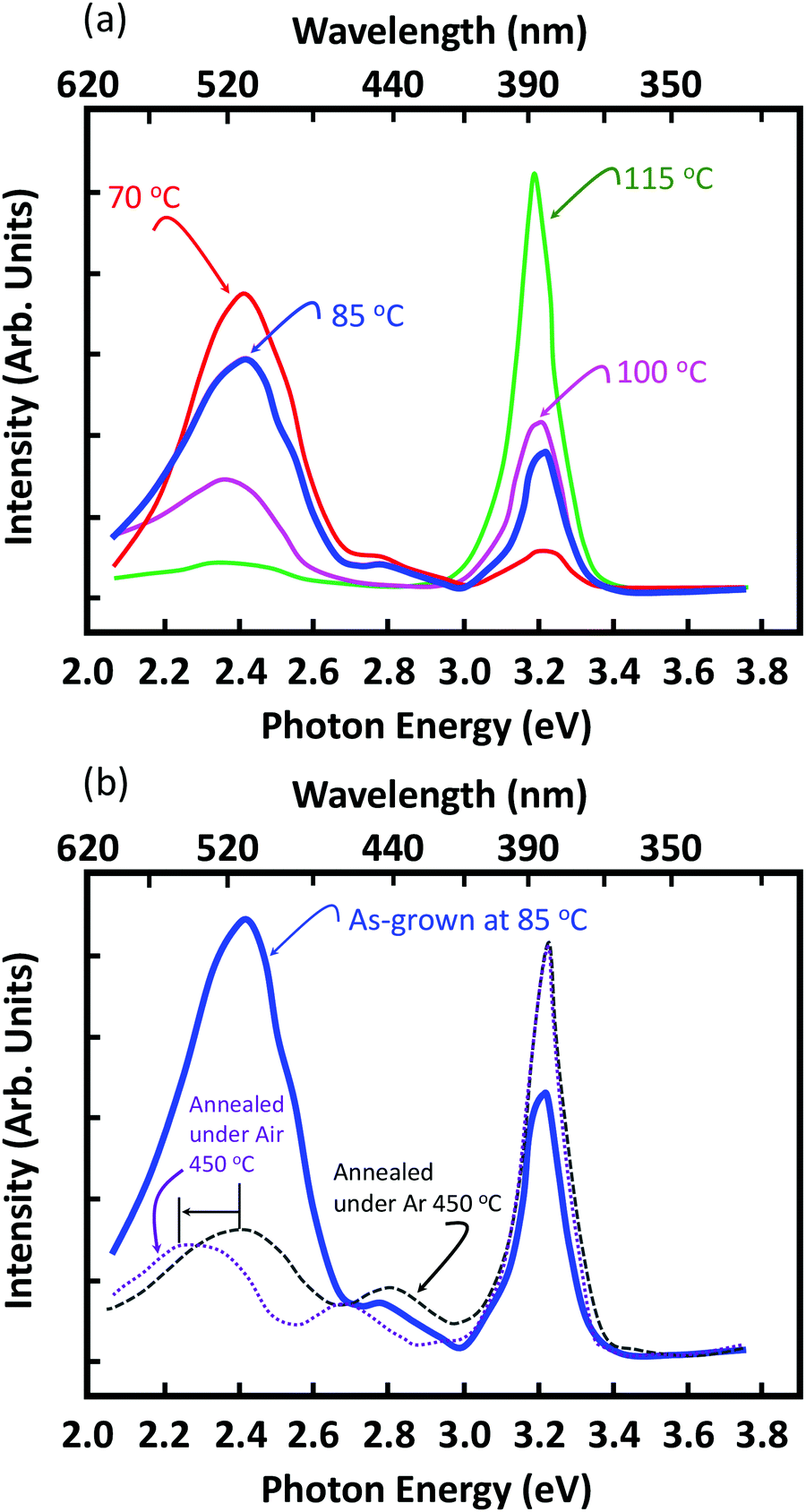 | ||
| Fig. 7 (a) PL spectra of (a) ZnO NRs grown at different temperatures, and (b) NRs grown at 85 °C thermally annealed at 450 °C for 1 h under air and an Ar atmosphere. | ||
It was previously demonstrated that surface coating and/or thermal annealing treatment could suppress the green emission (unlike the yellow one) efficiently.66,67 In order to verify this assumption, we performed an investigation on the influence of thermal annealing performed at 450 °C and at different atmospheres (air and argon). An increase in the UV emission is clearly observed. Second, this annealing results in a decrease of the defect emission (whose FWHM broadened while its intensity reduced, although not completely eliminated). Enhancing the UV emission and reducing the visible defect emission indicate that non-radiative defects are likely responsible for the low UV emission from as-grown ZnO nanorods prepared by a low hydrothermal method (i.e. 70 °C). Indeed, due to the low fabrication temperature associated with the hydrothermal method, a number of lattice defects, which can act as non-radiative recombination centers, might be expected.
More specifically, the diffusion of oxygen vacancies in the wurtzite structure mainly occurs in two ways, namely in-plane diffusion along the (001) plane where there are six symmetrical paths to the next neighboring oxygen atoms and out-of-plane diffusion where six equivalent paths exist with components parallel to the [0001] axis. Since the oxygen hcp lattice in the ZnO wurtzite crystal (c/a ∼ 1.606) is smaller than the ideal wurtzite structures (c/a ∼ 1.633), anisotropic diffusion of the defect states is dominant in ZnO. This causes migration of oxygen vacancy states from the bulk towards the surface of the NRs, resulting in a relative increase in the surface defect concentration. Upon annealing the NRs further, the non-stoichiometry at the surface of the NRs is compensated, thereby leading to a reduction of the green emission.
Based on the structural and optical properties of ZnO NRs AR layers, a simulation has been carried out using PC1D simulation tools to investigate the PV properties by simulating the current (I)–voltage (V) and incident photon-to-electron conversion efficiency (IPCE) data. In this work, the PCE and fill factor (FF) of the solar cells were calculated following a previous report.58–63Fig. 8a shows the simulated I–V characteristics and P–V curve of the Si solar cell based on ZnO NRs AR. The maximum Isc = 0.498 A, and Voc = 0.598 V with a conversion efficiency of about 15.48% (FF ∼ 52%) have been observed at a length of 1.1 μm for ZnO NRs. Solar cells with ZnO NRs 1.1 μm in length show the highest power of ∼0.24 W.
All the simulated data of solar cells are extracted by putting in the information of the ZnO NRs AR layer, which means vertically arranged NRs are crucial in this system. The plots of internal quantum efficiency (IQE) and external quantum efficiency (EQE) versus wavelength for the ZnO NRs AR-based Si solar cell are shown in Fig. 8b. The EQE of a Si solar cell based on ZnO NRs demonstrated over 80% absorption, covering a 400–1200 nm wavelength range, and the integrated photocurrent was consistent with the Isc extracted from the I–V curve. The absorption of blue photons might occur at the topmost part of the ZnO NRs, where the charge carriers are supposed to move across the entire length of the ZnO NRs to reach the p–n junction. Therefore, the enhancement of the PCE of a Si solar cell occurs by controlling the AR behavior of ZnO NRs. The diffusion coefficient and diffusion length are the critical factors to explain the good PCE and photocurrent of Si solar cells based on ZnO NRs AR, as they are associated with charge carrier transport upon light illumination.64 It is known that a shorter diffusion length results in a high recombination rate.64Fig. 8c depicts the plot of diffusion length and distance from the front of the AR, obtained by PC1D simulation. In all lengths of ZnO NRs AR, the diffusion lengths gradually increase up to 100 μm. Subsequently, saturation in diffusion length was obtained with the increase of distance from the front. This observation clearly deduces that the maximum limit of the diffusion length is 100 μm for all lengths of ZnO NRs, as illustrated in Fig. 8c. In this calculation, the thicknesses of the emitter regions are 15 μm, 24 μm, 24.78 μm, and 30 μm for 0.75 μm, 0.9 μm, 1.0 μm, and 1.1 μm lengths of ZnO NRs AR, respectively. From Fig. 8c, the ratios of the diffusion length to the thickness of the emitter are 6.66, 4.16, 4.03, and 3.33 for 0.75 μm, 0.9 μm, 1.0 μm, and 1.1 μm lengths of ZnO NRs, respectively. The lowest ratio value is related to a high penetration of dopant in the emitter. Moreover, the probability of charge collection at the interface of the N and P layers is linked with the diffusion length and size of the device, especially the emitter size.65–69 Suppose the thickness of the emitter is lower than the diffusion length, which results in a considerably high charge collection probability. As represented in Fig. 8c, the high diffusion length obtained by ZnO NRs AR is attributed to a higher probability of charge collection, resulting in the large collection of light-generated charge carriers at the p–n junction and high conduction to the cell. Hence, this simulation study reflects that the low-temperature solution method is highly feasible for growing vertically arranged ZnO NRs AR to fabricate the Si wafer-based solar cells.
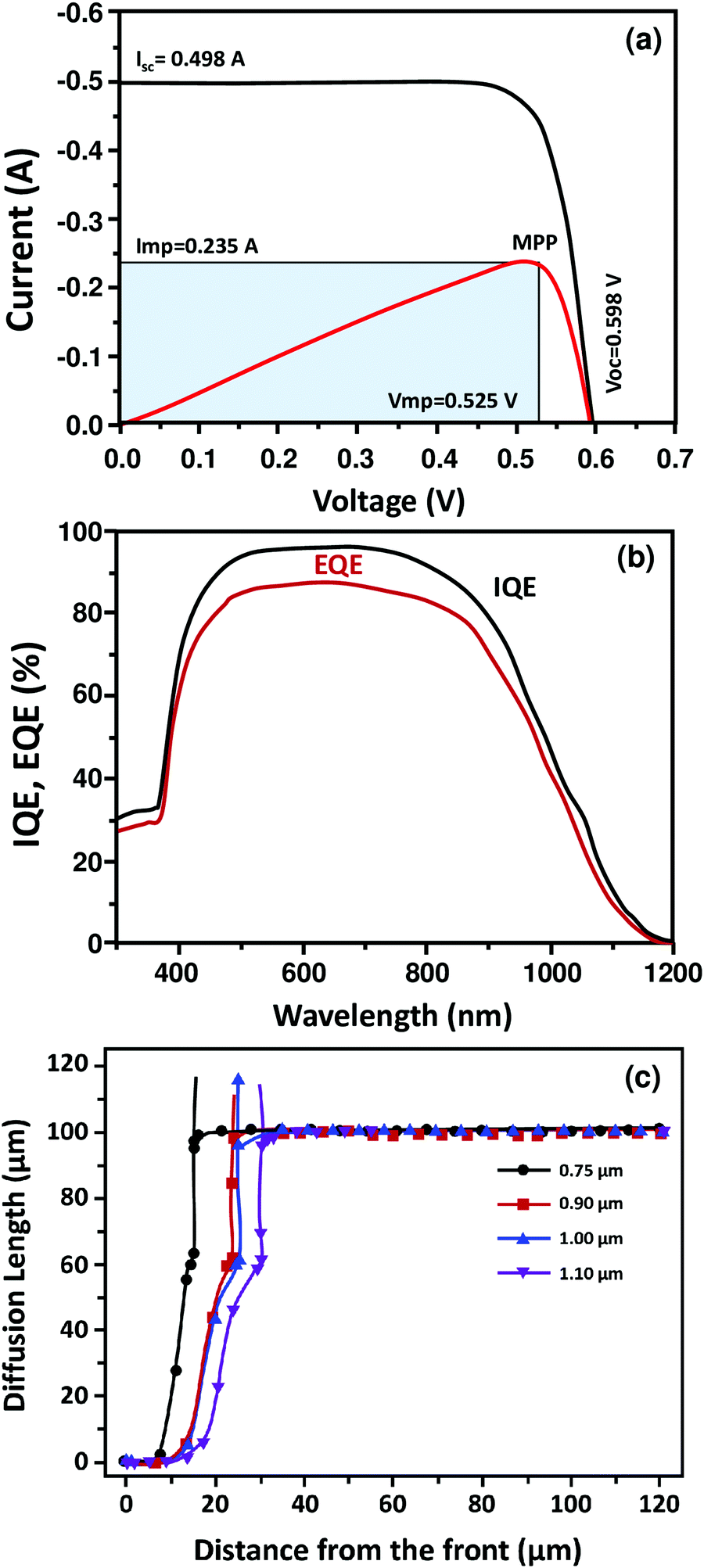 | ||
| Fig. 8 I–V curve with a power curve and (b) incident photon-to-electron conversion efficiency (IPCE) curve of Si solar cells based on ZnO NRs antireflection (AR). (c) Influence of variation in the length of ZnO NRs AR on the diffusion length. | ||
Conclusions
We varied the synthesis temperature and systematically investigated its effect on the morphology, crystal structure and optical properties of ZnO nanorod arrays using a suite of structural and optical characterization techniques. Our results showed a clear improvement of the ZnO crystallinity as the growth temperature increases from 70 °C to 85 °C, with a direct impact on the nucleation and growth rates of the morphology, orientation and optical properties of the ZnO rod arrays. The sample grown at 85 °C showed the c-axis orientation hexagonal phase of wurtzite ZnO as predominant. In addition, UV-Vis analysis has shown a nonlinear increase of the NBE with respect to the reaction temperature, where samples grown at 85 °C presented high UV absorption. We believe that this behavior could be correlated to the non-homogeneity of the morphology obtained at this specific reaction temperature where both uniform and highly dense ZnO NRs were obtained simultaneously, thereby leading to an increase in internal light scattering. PL analysis corroborated well the results obtained by XRD and demonstrated that an appropriate thermal annealing under air and/or inert atmosphere could be an efficient way to decrease the defect emission. The length of the ZnO NRs and the average reflectance were applied as input parameters in the PC1D simulation to instigate the PV properties of the solar cell. The optimum conversion efficiency of 15.48% has been achieved in ZnO NRs 1.1 μm in length by using this simulation tool. From this study, it has been confirmed that hydrothermal synthesis is an easy, facile and scalable process for the preparation of zinc nanorod structure-based Si solar cells, which demonstrated promising prospects in developing efficient and cost-effective hybrid c-Si solar cells.Conflicts of interest
The authors declare that they have no conflict of interest.Acknowledgements
We acknowledge funding from the Canada Foundation for Innovation for equipment and related operating funds and the Natural Science and Engineering Research Council (NSERC) of Canada for a Collaborative Research and Development project in partnership with MPB Communications Inc. and Plasmionique Inc., F. R. is also supported by an individual NSERC Discovery Grant. F. R. is grateful to the Canada Research Chairs program for funding and partial salary support. B. A. thanks the Qatar National Research Fund (QNRF, Member of Qatar Foundation) for the NPRP Grant #11S-0117-180330.References
- M. A. Boles, D. Ling, T. Hyeon and D. V. Talapin, The surface science of nanocrystals, Nat. Mater., 2016, 15, 141–153 CrossRef CAS PubMed.
- F. Rosei, Nanostructured surfaces: challenges and frontiers in nanotechnology, J. Phys.: Condens. Matter, 2004, 16, S1373–S1436 CrossRef CAS.
- A. K. Yetisen, A. F. Coskun, G. England, S. Cho, H. Butt, J. Hurwitz and S. H. Yun, Art on the Nanoscale and beyond, Adv. Mater., 2016, 28, 1724–1742 CrossRef CAS.
- J. N. Tiwari, R. N. Tiwari and K. S. Kim, Zero-dimensional, one-dimensional, two-dimensional and three-dimensional nanostructured materials for advanced electrochemical energy devices, Prog. Mater. Sci., 2012, 57, 724–803 CrossRef CAS.
- D. L. Leslie-Pelecky and R. D. Rieke, Magnetic Properties of Nanostructured Materials, Chem. Mater., 1996, 8, 1770–1783 CrossRef CAS.
- B. Y. Guo, J. Hu and L. Wan, Nanostructured Materials for Electrochemical Energy Conversion and Storage Devices, Adv. Mater., 2008, 20, 2878–2887 CrossRef.
- Y. T. Zhu, T. C. Lowe and T. G. Langdon, Performance and applications of nanostructured materials produced by severe plastic deformation, Scr. Mater., 2004, 51, 825–830 CrossRef CAS.
- L. Vayssieres, On the design of advanced metal oxide nanomaterials, Internet J. Nanotechnol., 2004, 1, 1–41 CrossRef CAS.
- M. H. Huang, S. Mao, H. Feick, H. Yan, Y. Wu, H. Kind and R. Russo, Room-temperature ultraviolet nanowire nanolasers, Science, 2001, 292, 1–4 CrossRef.
- S. Xu and Z. L. Wang, One-Dimensional ZnO Nanostructures: Solution Growth and Functional Properties, Nano Res., 2011, 4, 1013–1098 CrossRef CAS.
- B. Aïssa, M. Nedil, A. Belaidi, R. J. Isaifan, A. Bentouaf, C. Fautaux and D. Therriault, Photoluminescence quenching, structures, and photovoltaic properties of ZnO nanostructures decorated plasma grown single walled carbon nanotubes, J. Nanopart. Res., 2017, 19(157), 1–8 Search PubMed.
- B. Aïssa, C. Fauteux, D. Therriault and M. A. El Khakani, Structural and Photoluminescence Properties of laser processed ZnO/Carbon Nanotube Nanohybrids, J. Mater. Res., 2009, 24(11), 3313–3320 CrossRef.
- F. S. Kim, G. Ren and S. A. Jenekhe, One-Dimensional Nanostructures of π-Conjugated Molecular Systems: Assembly, Properties, and Applications from Photovoltaics, Sensors, and Nanophotonics to Nanoelectronics, Chem. Mater., 2011, 23, 682–732 CrossRef CAS.
- Z. L. Wang, Zinc oxide nanostructures: growth, properties and applications, J. Phys.: Condens. Matter, 2004, 16, 829–858 CrossRef.
- F. Rosei and R. Rosei, Atomic Description of Surface Processes: Diffusion and Dynamics, Surf. Sci., 2002, 500, 395–413 CrossRef CAS.
- X. Yu, T. J. Marks and A. Facchetti, Metal oxides for optoelectronic applications, Nat. Mater., 2016, 15, 383–396 CrossRef CAS PubMed.
- E. H. Nicollian and J. R. Brews, MOS (Metal Oxide Semiconductor) Physics and Technology, Wiley, New York, 2002 Search PubMed.
- L. Vayssieres, An aqueous solution approach to advanced metal oxide arrays on substrates, Appl. Phys. A: Mater. Sci. Process., 2007, 89, 1–8 CrossRef CAS.
- K. A. Wahid, W. Y. Lee, H. W. Lee, A. S. Teh, D. C.-S. Bien and I. A. Azid, Effect of seed annealing temperature and growth duration on hydrothermal ZnO nanorod structures and their electrical characteristics, Appl. Surf. Sci., 2013, 283, 629–635 CrossRef CAS.
- M. Yan, H. T. Zhang, E. J. Widjaja, R. P.-H. Chang, M. Yan, H. T. Zhang and R. P.-H. Chang, Self-assembly of well-aligned gallium-doped zinc oxide nanorods, J. Appl. Phys., 2003, 94, 5240–5246 CrossRef CAS.
- B. D. Yao, Y. F. Chan, N. Wang, B. D. Yao, Y. F. Chan and N. Wang, Formation of ZnO nanostructures by a simple way of thermal evaporation, Appl. Phys. Lett., 2002, 81, 757–759 CrossRef CAS.
- J. H. Liang, H. Y. Lai and Y. J. Chen, Morphology transition of ZnO films with DMZn flow rate in MOCVD process, Appl. Surf. Sci., 2010, 256, 7305–7310 CrossRef CAS.
- A. Moulahi, F. Sediri and N. Gharbi, Hydrothermal synthesis of nanostructured zinc oxide and study of their optical properties, Mater. Res. Bull., 2012, 47, 667–671 CrossRef CAS.
- L. Vayssieres, Growth of arrayed nanorods and nanowires of ZnO from aqueous solutions, Adv. Mater., 2003, 15, 464–466 CrossRef CAS.
- N. S. Ridhuan, K. Abdul Razak, Z. Lockman and A. Abdul Aziz, Structural and Morphology of ZnO Nanorods Synthesized Using ZnO Seeded Growth Hydrothermal Method and Its Properties as UV Sensing, PLoS One, 2012, 7, 1–15 CrossRef PubMed.
- A. Bahadur Yadav, P. V.-L. Parvathi and R. T. Shaik, Zero bias UV detection and precursor effect on properties of ZnO nanorods grown by hydrothermal method on SiO2/p-Si substrate, Thin Solid Films, 2019, 685, 343–352 CrossRef.
- T. Demes, C. Ternon, F. Morisot, D. Riassetto, M. Legallais, H. Roussel and M. Langlet, Mechanisms involved in the hydrothermal growth of ultra-thin and high aspect ratio ZnO nanowires, Appl. Surf. Sci., 2017, 410, 423–431 CrossRef CAS.
- N. Kumaresan, K. Ramamurthi, R. Ramesh Babu, K. Sethuraman and S. Moorthy Babu, Hydrothermally grown ZnO nanoparticles for effective photocatalytic activity, Appl. Surf. Sci., 2017, 418, 138–146 CrossRef CAS.
- Y. B. Kwon, S. W. Shin, H.-K. Lee, J. Y. Lee, J.-H. Moon and J. H. Kim, Formation of ZnO thin films consisting of nano-prisms and nano-rods with a high aspect ratio by a hydrothermal technique at 60 °C, Curr. Appl. Phys., 2011, 11, 197–201 CrossRef.
- S. D. Lee, Y. S. Kim, M. S. Yi, J. Y. Choi and S. W. Kim, Morphology Control and Electroluminescence of ZnO Nanorod/GaN Heterojunctions Prepared Using Aqueous Solution, J. Phys. Chem. C, 2009, 113, 8954–8958 CrossRef CAS.
- R. Pietruszka, B. S. Witkowski, E. Zielony, K. Gwozdz, E. Placzek-Popko and M. Godlewski, ZnO/Si heterojunction solar cell fabricated by atomic layer deposition and hydrothermal methods, Sol. Energy, 2017, 155, 1282–1288, DOI:10.1016/j.solener.2017.07.071.
- A. Kathalingam, V. Senthilkumar, S. Valanarasu and J.-K. Rhee, Shape-dependent electrical property of solution synthesized ZnO nanorods, Semicond. Sci. Technol., 2012, 27(10), 105006, DOI:10.1088/0268-1242/27/10/105006.
- H. Karaagac, M. Parlak, E. Yengel and M. S. Islam, Heterojunction solar cells with integrated Si and ZnO nanowires and a chalcopyrite thin film, Mater. Chem. Phys., 2013, 140, 382–390 CrossRef CAS.
- L. Mandal, S. Sadique Anwer Askari, M. Kumar and M. Imam, Analysis of ZnO/Si Heterojunction Solar Cell with Interface Defect, ed. U. Biswas, A. Banerjee, S. Pal, A. Biswas, D. Sarkar and S. Haldar, in Advances in Computer, Communication and Control. Lecture Notes in Networks and Systems, Springer, Singapore, 2019, vol 41, pp. 533–538 DOI:10.1007/978-981-13-3122-0_53.
- A. Kathalingam and J.-K. Rhee, Fabrication and characterization of solution processed n-ZnO nanowire/p-Si heterojunction device, J. Nanosci. Nanotechnol., 2012, 12(9), 6948–6954, DOI:10.1166/jnn.2012.6187.
- A. Kathalingam, H.-S. Kim, H.-M. Park, S. Valanarasu and T. Mahalingam, Effect of indium on photovoltaic property of n-ZnO/p-Si heterojunction device prepared using solution-synthesized ZnO nanowire film, J. Photon. Energy, 2015, 5(1), 053085 CrossRef.
- J. Zhang and W. Que, Preparation and characterization of sol gel Al-doped ZnO thin films and ZnO nanowire arrays grown on Al-doped ZnO seed layer by hydrothermal method, Sol. Energy Mater. Sol. Cells, 2010, 94, 2181–2186 CrossRef CAS.
- Y. Shi, Z. Yang, H. Cao and Z. Liu, Controlled c-oriented ZnO nanorod arrays and m-plane ZnO thin film growth on Si substrate by a hydrothermal method, J. Cryst. Growth, 2010, 312, 568–572 CrossRef CAS.
- Z. Qin, Q. Liao, Y. Huang, L. Tang, X. Zhang and Y. Zhang, Effect of hydrothermal reaction temperature on growth, photoluminescence and photoelectrochemical properties of ZnO nanorod arrays, Mater. Chem. Phys., 2010, 123, 811–815 CrossRef CAS.
- G. Hashmi, A. R. Akand, M. Hoq and H. Rahman, Study of the Enhancement of the Effciency of the Monocrystalline Silicon Solar Cell by Optimizing Effective Parameters Using PC1D Simulation, Silicon, 2018, 10, 1653–1660 CrossRef CAS.
- H. J. Moulahi, S. Lee, Y. Yu, S. M. Hong, H. C. Choi and M. Y. Choi, Low-temperature hydrothermal growth of ZnO nanorods on sol–gel prepared ZnO seed layers: Optimal growth conditions, Thin Solid Films, 2012, 524, 144–150 CrossRef.
- L. Vayssieres, K. Keis, A. Hagfeldt and S. E. Lindquist, Purpose-Built Anisotropic Metal Oxide Material: 3D Highly Oriented Microrod Array of ZnO, J. Phys. Chem. B, 2001, 105, 3350–3352 CrossRef CAS.
- I. M. Fisher and D. A. Smith, Grain Boundary Migration and the texture of films, Textures Microstruct., 1991, 13, 91–99 CrossRef.
- N. Ekthammathat, S. Thongtem, T. Thongtem and A. Phuruangrat, Characterization and antibacterial activity of nanostructured ZnO thin films synthesized through a hydrothermal method, Powder Technol., 2014, 254, 199–205 CrossRef CAS.
- D. Polsongkram, P. Chamninok, S. Pukird, L. Chow, O. Lupan, G. Chai, H. Khallaf, S. Park and A. Schulte, Effect of synthesis conditions on the growth of ZnO nanorods via hydrothermal method, Phys. B, 2008, 403, 3713–3717 CrossRef CAS.
- M. Guo, P. Diao, X. Wang and S. Cai, The effect of hydrothermal growth temperature on preparation and photoelectrochemical performance of ZnO nanorod array films, J. Solid State Chem., 2005, 178, 3210–3215 CrossRef CAS.
- S. Xu, C. Lao, B. Weintraub and Z. L. Wang, Density-controlled growth of aligned ZnO nanowire arrays by seedless chemical approach on smooth surfaces, J. Mater. Res., 2008, 23, 2072–2077 CrossRef CAS.
- X. Q. Zhao, C. R. Kim, J. Y. Lee, J. H. Heo, C. M. Shin, H. Ryu and X. W. Sun, Effects of buffer layer annealing temperature on the structural and optical properties of hydrothermal grown ZnO, Appl. Surf. Sci., 2009, 255, 4461–4465 CrossRef CAS.
- A. Alshanableh, C. C. Yap, S. T. Tan, H. B. Lee, C. H. Tan, R. T. Ginting and M. H.-H. Jumali, Novel hydrothermal approach to functionalize self-oriented twin ZnO nanotube arrays, Mater. Lett., 2016, 165, 75–78 CrossRef CAS.
- X. S. Fang, C. H. Ye, L. D. Zhang and T. Xie, Twinning-mediated growth of Al2O3 nanobelts and their enhanced dielectric responses, Adv. Mater., 2005, 17, 1661–1665 CrossRef CAS.
- B. D. Cullity and S. R. Stock, Element of X-ray Diffraction, Prentice Hall, New Jersey, 2001 Search PubMed.
- M. F. Cerqueira, T. Viseu, J. Ayres De Campos, A. G. Rolo, T. De Lacerda-Aroso, F. Oliveira, I. Bogdanovic-Radovic, E. Alves and M. I. Vasilevskiy, Raman study of insulating and conductive ZnO:(Al, Mn) thin films, Phys. Status Solidi A, 2015, 212, 2345–2354 CrossRef CAS.
- Y. Caglar, S. Ilican, M. Caglar, F. Yakuphanoglu, J. Wu, K. Gao, P. Lu and D. Xue, Influence of heat treatment on the nanocrystalline structure of ZnO film deposited on p-Si, J. Alloys Compd., 2009, 481, 885–889 CrossRef CAS.
- Y. Zhao, Y. Jiang and Y. Fang, The influence of substrate temperature on ZnO thin films prepared by PLD technique, J. Cryst. Growth, 2007, 307, 278–282 CrossRef CAS.
- R. Vettumperumal, S. Kalyanaraman and R. A. Thangavel, comparative study of structural, surface morphology and optical properties of Na and Mg codoped ZnO nanocrystalline thin films prepared using sol–gel spin coating technique, J. Mol. Struct., 2014, 1059, 61–67 CrossRef CAS.
- S. Ben Yahia, L. Znaidi, A. Kanaev and J. P. Petitet, Raman study of oriented ZnO thin films deposited by sol–gel method, Spectrochim. Acta, Part A, 2008, 71, 1234–1238 CrossRef.
- O. Lupan, T. Pauport, I. M. Tiginyanu, V. V. Ursaki, V. Sontea, L. K. Ono and L. Chow, Comparative study of hydrothermal treatment and thermal annealing effects on the properties of electrodeposited micro-columnar ZnO thin films, Thin Solid Films, 2011, 519, 7738–7749 CrossRef CAS.
- A. Kathalingam and H.-S. Kim, Annealing induced p-type conversion and substrate dependent effect of n-ZnO/p-Si heterostructure, Mater. Lett., 2017, 196, 30–32 CrossRef CAS.
- A. Kathalingam, S. Valanarasu, A. M. Ali, M. A. Sayed, W. Yang and H.-S. Kim, Photosensing effect of indium-doped ZnO thin films and its heterostructure with silicon, J. Asian Ceram. Soc., 2022, 10(1), 108–119 CrossRef.
- T. Wermelinger and R. Spolenak, Symmetry of residual stress fields of ZnO below an indent measured by three-dimensional Raman spectroscopy, J. Appl. Phys., 2009, 106, 64907 CrossRef.
- I. D. Wolf, Micro-Raman spectroscopy to study local mechanical stress in silicon integrated circuits, Semicond. Sci. Technol., 1996, 11, 139–154 CrossRef.
- L. Liao, D. H. Liu, J. C. Li, C. Liu, Q. Fu and M. S. Ye, Synthesis and Raman analysis of 1D-ZnO nanostructure via vapor phase growth, Appl. Surf. Sci., 2005, 240, 175–179 CrossRef CAS.
- K. A. Salman, Effect of surface texturing processes on the performance of crystalline silicon solar cell, Sol. Energy, 2017, 147, 228–231 CrossRef CAS.
- Z. Z. Bandic, P. M. Bridger, E. C. Piquette and T. C. McGill, Electron diffusion length and lifetime in p-type GaN, Appl. Phys. Lett., 1998, 73, 3276–3278 CrossRef CAS.
- A. B. Djurisic, W. C.-H. Choy, V. A.-L. Roy, Y. H. Leung, C. Y. Kwong, K. W. Cheah, T. K. Gundu Rao, W. K. Chan, H. F. Lui and C. Surya, Adv. Funct. Mater., 2004, 14, 856 CrossRef CAS.
- K. Vanheusden, W. L. Warren, C. H. Seager, D. R. Tallant, J. A. Voigt and B. E. Gnade, J. Appl. Phys., 1996, 79, 7983 CrossRef CAS.
- K. Vanheusden, C. H. Seager, W. L. Warren, D. R. Tallant and J. A. Voigt, Appl. Phys. Lett., 1998, 68, 403 CrossRef.
- X. Cai, X. Zhou, Z. Liu, F. Jiang and Q. Yu, An in-depth analysis of the silicon solar cell key parameters’ optimal magnitudes using PC1D simulations, Optik, 2018, 164, 105–113 CrossRef CAS.
- M. Iqbal, M. M. Nauman, F. U. Khan, P. E. Abas, Q. Cheok, A. Iqbal and B. Aissa, Vibration-based piezoelectric, electromagnetic, and hybrid energy harvesters for microsystems applications: A contributed review, Int. J. Energy Res., 2021, 45(1), 65–102 CrossRef CAS.
| This journal is © The Royal Society of Chemistry 2022 |