DOI:
10.1039/D2MA00485B
(Paper)
Mater. Adv., 2022,
3, 5930-5940
Enhancing the third-order nonlinearity and crystallinity by selenium incorporation in tin sulfide films (SnS1−xSex) for optoelectronic applications
Received
29th April 2022
, Accepted 3rd June 2022
First published on 6th June 2022
Abstract
Thin films of SnS1−xSex with varying Se (x = 0, 0.1, 0.15, 0.2, 0.25) contents were deposited by the thermal evaporation method on glass substrates at room temperature. The crystalline nature of the films is verified using structural characterization techniques such as X-ray diffraction and Raman analysis. The crystallinity increased with Se concentration. The nanoflake-like structure with an increase in size and density upon Se addition is observed from the morphology study through field emission scanning electron microscopy. The energy-dispersive X-ray analysis confirmed the elemental % in different films. The transmittance data were recorded in the range of 900–1100 nm by UV-Vis spectroscopy and used to evaluate the linear/nonlinear optical properties. The transmission percentage decreased with the doping of Se in the SnS binary compound. The absorption and extinction coefficients were enhanced with Se content. The bandgap value decreased with the doping concentration. The optical energy gap is used to evaluate the static refractive index using Dimitrov and Sakka's relation. The value of the static refractive index increased with Se content, which further helped to enhance the nonlinear optical parameters. The nonlinear parameters such as the nonlinear refractive index and third-order nonlinear susceptibility increased with the Se concentration. The theoretically calculated physical parameters like the average heat of atomization decreased with Se content. Tuning of nonlinear and linear properties by varying the selenium doping content in SnS1−xSex films will be useful in many photonic and optoelectronic devices.
1. Introduction
Recently, scientists have focused on non-toxic, low-cost semiconductor materials to improve the absorber layers used in photo-sensing devices. Typically, materials like metal chalcogenides,1 monochalcogenides,2 graphene,3 and phosphorene4 have inherent applications in the fields of photovoltaics and optoelectronics. Among them, metal chalcogenides are widely used materials having the most favourable semiconducting properties with a low bandgap for application in advanced electronics and photonic devices.5 Among metal chalcogenides, tin chalcogenide semiconductors have potential applications in thermoelectric devices, optoelectronics, memory switching devices,6 photovoltaics, lithium-ion batteries,7 and photocatalysts.8 Tin chalcogenides are favourable candidates to be used in high-performance photodetectors for their exceptional absorption coefficient, carrier mobility, and suitable bandgap (0.81–2.31 eV).9,10 Recently, these materials have attracted more attention due to their non-toxic, low-cost, and abundant nature.11 Layered tin chalcogenides also exhibit excellent anisotropic properties. Previously reported tin chalcogenides like SnSe and SnS possess anisotropic electrical conductivity due to the difference in the electronic masses of electrons and holes along the axes.12 SnS compounds exhibit layered orthorhombic structures with favorable direct and indirect bandgap values of 1.2 to 1.7 eV and 1 to 1.1 eV, respectively, for potential applications in photovoltaic cells.13 Tin sulphide has favorable properties like p-type electrical conductivity, an orthorhombic crystal structure, and a significant absorption coefficient for making absorber layers in the preparation of thin-film heterojunction solar cells.14,15 The constituent atoms Sn and S are tightly bonded by weak van der Waals forces and form a chemically inert surface without any surface dangling bonds and density of states, thus increasing the transparency and making the surface chemically and environmentally stable.16 SnS and SnSe compounds have been studied on a large scale by using various synthesis methods, such as chemical/physical vapor deposition,17,18 sputtering, solvothermal,19 and pulsed laser deposition.20 The photodetectors made from the compounds of SnSe and SnS exhibit large values of responsivity (102–104 A W−1) and average external quantum efficiencies (EQEs). For the improvement of SnSe- and SnS-based photodetectors, several approaches like alloy engineering and van der Waals heterostructures are adopted. Xia et al. have reported the use of a combination of both alloy engineering and van der Waals heterostructures for the SnS–SnSxSe1−x core–shell structure.21 Alloy engineering effectively enhances the photodetection properties and tunes the semiconductor's band structure and carrier types. Recently, different techniques such as doping and annealing were used to control the carrier concentration and conductivity of tin sulphide to improve the performance of SnS based solar cells. Doping of some metal elements like Sb, Bi, Cu,22 Ag,23 In,24 and Se25 has been reported for enhancing the properties of SnS.26,27 The hole concentration is increased by doping of Se into SnS. Yu et al. have reported that Se doping into the SnS host matrix increases the photoconductivity, hole concentration, and conversion efficiency and reduces the optical bandgap.28 This suggests that Se doped SnS has more potential optoelectronic applications than pure SnS. The SnS1−xSex matrix involves higher charge carrier transport phenomena than SnS, with a decrease of the S content.29,30 Thus, it is possible to improve both the electronic and optoelectronic properties of the as-prepared SnS and SnSe crystals by the alloying technique. Furthermore, the Sn–S–Se matrix exhibits an energy gap value in the order of the optimum energy gap for solar cells and a large absorbance near the infrared region, making it a suitable material for solar cells and optoelectronic applications.31,32 Moreover, for the SnS0.5Se0.5 system, the on/off ratio can be enhanced up to 2.10 × 10² at room temperature, which is two times larger than those of SnS and SnSe.29 In view of many optoelectronic properties and potential futuristic applications, we have synthesized and investigated the properties of Se doped SnS, i.e. SnS1−xSex (x = 0.1, 0.15, 0.2, 0.25).
In this study, nanostructured SnS and Se doped SnS bulk alloys were prepared by the melt quenching method, and the corresponding films were coated on glass substrates by the thermal evaporation process. The influence of the Se content in SnS on optical and structural properties was studied through different experiments. The present work aims to explore the tuning of nonlinear/linear optical properties like the nonlinear refractive index, third-order optical susceptibility, refractive index, optical bandgap, etc. in SnS1−xSex thin films at different selenium concentrations. The phase formation and crystallinity were analyzed by X-ray diffraction (XRD) and Raman spectroscopy. The energy dispersive X-ray (EDX) analysis was used for compositional analysis, and field emission scanning electron microscopy (FESEM) was used to analyze the surface morphology changes. The nonlinear/linear optical parameters of Se doped and undoped SnS thin films were calculated from the UV-visible spectroscopy data. The theoretical physical parameters like the heat of atomization, average coordination number, and bond strength were calculated and well discussed.
2. Experimental work
2.1. Preparation of thin films
The bulk SnS1−xSex (x = 0, 0.1, 0.15, 0.2, 0.25) samples were prepared by the melt quenching process. The high purity (99.999% Sigma-Aldrich) elements of Sn, Se, and S were used to prepare the bulk sample. Stoichiometric amounts of constituent elements were sealed in an evacuated quartz ampoule at a 10−5 torr vacuum. The quartz ampoule was placed in a furnace, and the temperature was maintained at 900 °C for 24 h with at a rate of 3 °C to 4 °C per minute. After 24 h of melting, the ampoule was removed and immediately placed in a cold water bath to avoid crystallization. The obtained bulk sample was ground to powder form and used to prepare the thin film. The thin film was deposited on a Corning glass substrate by the thermal evaporation technique using a HINDI-HIVAC Model 12A4D vacuum coating unit under a vacuum of 10−5 torr. The films were coated at a rate of 0.5 nm s−1 to a thickness of ∼800 nm which was measured using a thickness monitor.
2.2. Characterization methods
The structural analysis of SnS1−xSex films was done with a Bruker D8 Advance X-ray diffractometer with a copper target used as the X-ray source. The source has a wavelength of 0.154 nm. The X-ray spectra were recorded in the scan range of 10° to 80° at a scanning speed of 1° min−1 and a step size of 0.02° s−1. The surface morphology was examined using a Carl Zeiss Ultra 55 FESEM unit. An EDX system was used to analyze the elemental compositions. Surface scans were taken with a sample size of 1 × 1 cm2 at 3–4 positions at 20 kV and 40 mA emission current with a pressure of 2 × 10⁻⁷ torr. Raman data were recorded using a LabRAM HR system in the range of 100–400 cm−1 by using an argon laser source and a backscattered CCD detector. A Bruker Optics IFS66v/S UV-visible spectrometer was used to record the optical transmission and absorption spectra in the visible range.
3. Results analysis and discussion
3.1. XRD study
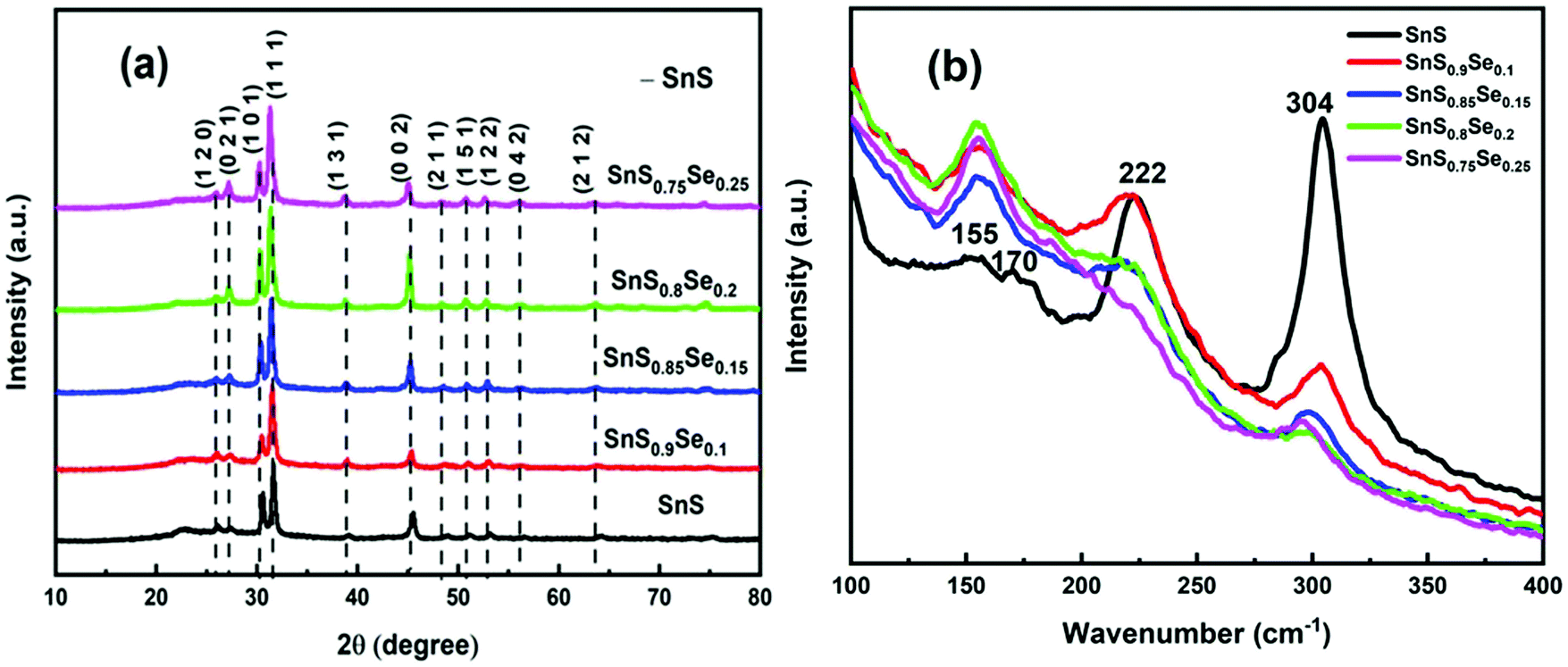
The XRD pattern of SnS1−xSex nanoflakes with different Se doping concentrations (x = 0, 0.1, 0.15, 0.2, 0.25) is shown in Fig. 1(a), which reveals the crystalline nature of all the samples. The diffraction peaks of all the samples matched well with the International Center for Diffraction Data (ICDD). From the analysis, it is observed that the crystalline peaks belong to the orthorhombic phase of tin sulphide, having the reference code ICDD PDF No. 00-39-0354. From the X-ray diffraction spectra, the prominent peak at 2θ ∼ 31.68° is due to the reflection of the (1 1 1) plane which has the largest spacing in orthorhombic tin sulphide. The peak intensity of crystalline phases increased with the increase of Se doping, indicating an increase in crystallinity. From the X-ray diffraction analysis, there is no phase change and no additional peaks are obtained in the SnS phase. But the crystalline peaks shifted towards the lower angle side due to the expansion of lattice parameters with an increase of Se doping, which satisfies Vegard's law.1 According to Vegard's law, the dopant alone cannot produce individual peaks, except the host peak, but it can generate acceptable shifts in the position of the host peak. All the calculated microstructural parameters are tabulated in Table 1.
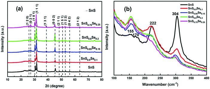 |
| | Fig. 1 (a) XRD pattern presenting different phases and (b) Raman spectra of SnS1−xSex (x = 0, 0.1, 0.15, 0.2, 0.25) thin films. | |
Table 1 Microstructural parameters of undoped and Se doped SnS1−xSex thin films
| Sample |
Crystallite size (D) in m (× 10−8) |
Dislocation density (δ) in m−2 (× 1015) |
Strain (ε) (× 10−4) |
N (1 m−2) (× 1017) |
| SnS |
1.668 |
3.591 |
64.5 |
1.721 |
| SnS0.9Se0.1 |
1.679 |
3.546 |
68 |
1.689 |
| SnS0.85Se0.15 |
1.691 |
3.493 |
67.1 |
1.659 |
| SnS0.8Se0.2 |
1.876 |
2.840 |
58.4 |
1.211 |
| SnS0.75Se0.25 |
1.737 |
1.737 |
66 |
1.524 |
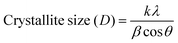
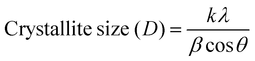
Scherrer's equation33 is used to calculate the average crystallite size (D):
| |  | (1) |
where the Scherrer constant
k = 0.94, the Cu Kα line
λ = 0.154 nm,
β is the full-width at half-maximum in radians, and ‘
θ’ is the Bragg angle. Furthermore, the incorporation of Se affects the microstructural parameters like lattice strain (ε), dislocation density (
δ), and the number of crystallites per unit surface area (
N). The microstructural parameters were calculated using the following relations:
34| | 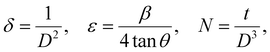 | (2) |
where ‘
t’ is the film thickness. The evaluated quantities are presented in
Table 1, which shows that the average crystallite size increased with the increase of Se doping in the SnS film up to 0.2 and then decreased with further Se doping as reported by Kafashan
et al.35 The increase of crystallinity might have occurred for the formation of new nucleation centers from the dopant atoms. However, further Se doping results in saturation nucleation and leads to a mismatch in the SnS lattice, resulting in decreased crystallinity. There is a decrease in strain and dislocation density with Se doping, which ensures the increase in the crystallinity of the compound. The
N value decreases with Se doping.
3.2. Raman analysis
Raman spectroscopy is an important characterization technique which helps to analyze information regarding molecular interactions, chemical structures, and crystal phases. The vibrational band analysis gives important information about phase transitions and structural rearrangements due to Se doping. The Raman data of the SnS1−xSex film in the range of 100–400 cm−1 are shown in Fig. 1(b). The Raman bands of the as-prepared tin sulphide thin film are centered at 155, 170, 222, and 304 cm−1, respectively. Li et al. have reported the presence of a Raman band at 150 cm−1 for the Ag mode of SnSe, which shows that the observed band at 155 cm−1 can be attributed to the Ag phase of SnSe.18 The intensity of the SnSe band with the Ag mode increased with the concentration of Se doping. The 170 cm−1 vibrational band is due to the B3g mode of SnS.36 The B3g mode that appeared at 170 cm−1 disappeared for all other Se doped samples. Tian et al. reported the Ag mode of the SnS band that appeared at a peak position of 218.7 (cm−1).17 Thus, the 222 cm−1 band is assigned to the Ag mode of SnS, whose intensity decreased with the incorporation of Se. From the Raman spectra, the most intense peak at 304 cm−1 is probably due to the Sn2S3 phase, as reported earlier by Reddy et al., in which the band intensity decreased with Se doping.37 Thus, from the Raman spectra, it is observed that the vibrational bands become broader and show a redshift with an increase of Se doping concentration compared to the undoped SnS sample. Thus, the formation of different bands and changes in their intensity and position led to structural changes due to the variation of Se in SnS1−xSex samples.
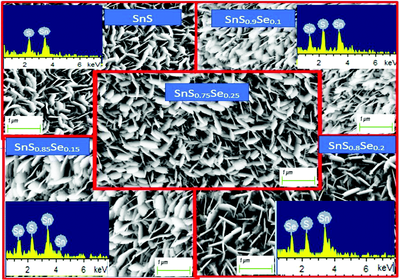
3.3. FESEM and EDX studies
The 1 μm FESEM images of the SnS1−xSex films with different Se concentrations are shown in Fig. 2. Remarkable changes in the surface morphology of SnS1−xSex films are observed due to the incorporation of Se in the SnS film. From the figure, it can be observed that the tin sulphide sample shows a densely packed nanoflake-like morphological structure. The columnar grain growth of SnS might have been caused by the 2D growth nature of SnS.38 It can be clearly seen that the grain size increased with the increase in the Se concentration. The improvements in the uniformity and packing of grains are due to the Se incorporation which results in an enhancement in reflectance properties.35 But a higher doping concentration of Se can lead to a decrease in the grain size again. These morphological variations may be due to Se incorporation. From the XRD data, the intensity of the peak at (1 1 1) increased with Se incorporation, but for a higher amount of Se incorporation (x = 0.25), the peak intensity decreased. A similar trend was observed for the FESEM grain size. Thus, there is a good correlation between XRD and FESEM data.
 |
| | Fig. 2 FESEM images of SnS1−xSex (x = 0, 0.1, 0.15, 0.2, 0.25) thin films and their corresponding EDX images (inset). | |
The EDX images show the presence of all the elements (Sn, S, Se) in the investigated SnS1−xSex films without any contamination. The EDX and FESEM images are shown in Fig. 2, which represent the different peaks corresponding to their respective elements. Furthermore, the related atomic percentage of the elements was calculated from the peak intensities and the area under the peak of the corresponding elements. A systematic increase in the atomic percentage of the Se content is found from the EDX analysis, which is in accordance with the increase of the Se dopant in the SnS film.
3.4. Optical properties
3.4.1. Transmission (T), absorption coefficient (α), extinction coefficient (k), bandgap (Eg), and Urbach energy (Eu).
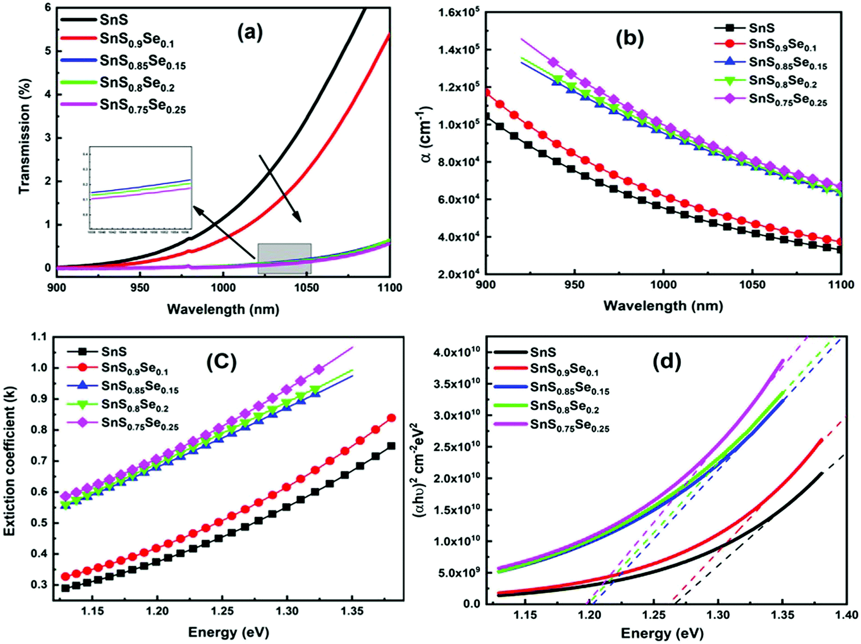
Transmission (T) is a basic optical parameter that indicates the % of transmitted light through an optical medium. Materials with a high transmission are used in many potential applications like optoelectronic sensors and photonic devices. Fig. 3(a) shows the transmittance spectra of ternary SnS1−xSex films in the wavelength range of 900–1100 nm. The transmission percentage decreased with Se doping. The films become more absorbing for which there is a decrease in the transmittance with an increase in Se doping. The decrease in transmittance is also due to the crystallization of the film structure by increasing the crystallite size with Se doping as observed from the XRD study. The absorption edge of the film showed a redshift with the Se content. The addition of ‘Se’ atoms increases the interconnection between the film atoms as they form more heteropolar bonds in the film. In addition, the Se element has a lower bandgap than S. Thus, incorporation of Se in the SnS film enhances the absorption of the samples and leads to a redshift of the absorption edge. Similar results have also been reported by Banotra et al.32 According to their explanation, the decrease in the transmittance percentage is ascribed to the grain boundaries and lattice defects that exist in the film due to the interaction of Se ions.
 |
| | Fig. 3 (a) Transmittance spectra of SnS1−xSex (x = 0, 0.1, 0.15, 0.2, 0.25) thin films, (b) change in the absorption coefficient (α) with Se concentration, (c) variation of the extinction coefficient (k), and (d) estimation of the direct bandgap for different Se concentration films. | |
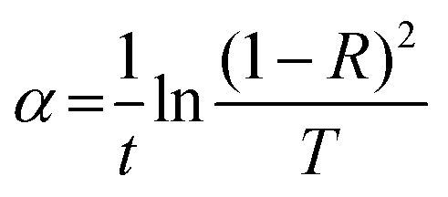
The absorption coefficient (α) gives the ability to absorb electromagnetic radiation when it passes through a material. The information regarding the band structure and optical bandgap of the film can be extracted by using the absorption coefficient data. The ‘α’ value is calculated by using the formula:39
| |  | (3) |
where ‘
t’ is the film thickness (∼800 nm), ‘
T’ represents the transmittance and ‘
R’ represents the reflectance of the films. The absorption coefficient graph of the SnS
1−xSe
x films is shown in
Fig. 3(b), which reveals the α value in the order of 10
4–10
5 cm
−1 and is reduced with wavelength. The decrease of ‘
α’ with wavelength indicated an increase in the transparency of the film at a higher wavelength and became suitable for light waves to propagate faster and easier. Moreover, the α value increased with the increase of the Se doping concentration and reached the order of 10
5 cm
−1 which is more than 2–3 × 10
4 cm
−1 as reported.
40 Therefore, the sample can be used as an excellent solar absorber in the field of photovoltaics with a significantly lower thickness.
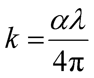
The extinction coefficient (k) is calculated in terms of ‘α’ and ‘λ’ by using the relation:41
| |  | (4) |
The surface smoothness and homogeneity of the sample were analyzed from the extinction coefficient (
k) data.
Fig. 3(c) shows the variation of the extinction coefficient with photon energy. It is noticed that the extinction coefficient increased with the incident energy as well as with the Se doping concentration. The increase in ‘
k’ with energy and its decrease with wavelength represent the light dispersion and drop in absorption, respectively. The low ‘
k’ value for the pure SnS sample indicates a smooth and homogeneous surface of the films. But, with an increase in Se doping, the ‘
k’ value increased, which shows a decrease in surface smoothness as confirmed by the structural analysis.
The optical bandgap energy (Eg) plays an essential role in selecting the semiconducting materials for potential applications. According to Tauc, the energy required to transport an electron through a forbidden bandgap depends on the intrinsic behavior of the film and the photon energy in semiconducting materials.42 For a semiconducting material, the absorption strength of the incident electromagnetic waves depends on the difference between bandgap energy (Eg) and incident photon energy (hν). Here, Tauc's formula is used to calculate the energy gap in the high absorption region (α ≥ 104 cm−1) by using43
where ‘
ν’ represents the incident frequency, ‘
B’ is the band tail parameter which depends upon the transition probability, and ‘
m’ is the transition mode power factor which depends on the type of electronic transition. For different transitions, ‘
m’ has different values,
i.e.,
m = 1/2 for direct allowed transitions, 2 for indirect allowed transitions, 3/2 for direct forbidden transitions, and 3 for indirect forbidden transitions. As per the Tauc rule, indirect transitions are observed for amorphous materials and direct allowed transitions for crystalline materials. Since both undoped and selenium doped films show a crystalline nature,
m = 1/2 was substituted in
eqn (5) to evaluate the direct allowed energy gap, and the plot between (
αhν)
2vs. hυ is shown in
Fig. 3(d). The
Eg value is taken from the intercept of the graph, and the slope gives the Tauc parameter (
B). The obtained values of both ‘
Eg’ and ‘
B’ are presented in
Table 2. It is found that the bandgap value decreased from 1.265 ± 0.001 eV to 1.197 ± 0.001 eV with an increase in Se%. Wang
et al. also reported similar results, where the optical bandgap decreased from 1.15 to 1.01 eV with Se doping.
44 The material having a small bandgap can block both visible light and infrared light transmission. Moreover, these materials possess a unique ability to filter the ultraviolet part from electromagnetic radiation. This property makes thin films of smaller bandgaps suitable for solar applications and thermal systems.
45 The slope of the graph gives the ‘
B’ value, which is inversely proportional to the degree of disorder. It is observed from
Table 2 that ‘
B’ increases with selenium doping.
Table 2 Optical parameters of SnS1−xSex thin films
| Estimated optical parameters |
SnS |
SnS0.9Se0.1 |
SnS0.85Se0.15 |
SnS0.8Se0.2 |
SnS0.75Se0.25 |
| Optical band gap (direct Eg) in eV |
1.265 ± 0.001 |
1.261 ± 0.002 |
1.202 ± 0.001 |
1.198 ± 0.001 |
1.197 ± 0.001 |
| Tauc parameter (B2) in cm−2 eV−2 |
1.797 × 10¹¹ |
2.161 × 10¹¹ |
2.184 × 10¹¹ |
2.213 × 10¹¹ |
2.465 × 10¹¹ |
| Urbach energy (Eu) in eV |
0.218 |
0.219 |
0.295 |
0.303 |
0.282 |
| Static refractive index (n0) |
3.150 |
3.154 |
3.199 |
3.202 |
3.203 |
| Dielectric constant of the lattice (ε∞) |
9.924 |
9.945 |
10.235 |
10.254 |
10.261 |
| First-order nonlinear susceptibility (χ1) |
0.710 |
0.712 |
0.735 |
0.736 |
0.737 |
| Third-order nonlinear susceptibility (χ3) |
4.333 × 10⁻¹¹ |
4.374 × 10⁻¹¹ |
4.968 × 10⁻¹¹ |
5.009 × 10⁻¹¹ |
5.024 × 10⁻¹¹ |
| Nonlinear refractive index (n2) |
5.182 × 10⁻¹⁰ |
5.226 × 10⁻¹⁰ |
5.851 × 10⁻¹⁰ |
5.895 × 10⁻¹⁰ |
5.910 × 10⁻¹⁰ |
| Optical electronegativity (ηopt) |
1.6874 |
1.6869 |
1.6809 |
1.6805 |
1.6803 |
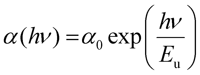
According to Urbach, near the absorption edge of semiconducting materials, there is an exponential region that describes the width of the band tail of the material. This band tail represents the localized states.46 The absorption coefficient for most of the semiconducting material depends on ‘hν’ near the band edge, satisfying the Urbach empirical formula:47
| |  | (6) |
where ‘
α0’ is the constant value corresponding to the absorption coefficient at the band gap energy and ‘
Eu’ is the Urbach energy. The
Eu parameter measures the degree of disorder in the material, which is the inverse of the slope obtained from the graph between
hυ and ln(
α/
α0). The obtained
Eu values are tabulated in
Table 2, which shows an increasing trend, while the optical bandgap decreases with selenium doping. This might be due to the incorporation of selenium, which increases the localized states within the bandgap region. Davis and Mott's
48 model infers that the localized states within the band structure are the reason for the reduction of the bandgap. Thus, our results seem to have a good agreement with Davis and Mott's discussion.
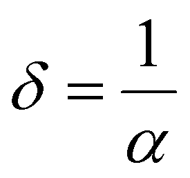
3.4.2. Optical density and skin depth.
Optical density (OD) is associated with the absorption of light, which indicates the absorbing power of a material towards electromagnetic radiation. The optical density is proportional to both the thickness and concentration of the absorbing material. The optical density of SnS1−xSex is calculated by using the simple formula:49 OD = α × t, where ‘t’ is the film thickness. Fig. 4(a) shows the change in OD with wavelength. It is observed that the variation of OD, with either wavelength or incident energy, shows a similar behaviour to the absorption coefficient where the thickness of all the samples is constant.50 In the intense absorption spectral regions, all the energy that enters the thin film is either absorbed or reflected. Here, skin depth is one of the important parameters which is related to the absorption of photons within the thin film texture. The photon density decreased in an exponential way from the surface towards the midway of the film. This happens due to many factors like the film density, surface morphology, refractive index, and microstructure of the films. Skin depth (δ) is defined as the thickness at which the density of photons becomes 1/e of the value at the surface. The conductivity of the film and the incident photon energy also affect the value of skin depth. As the conductivity of the semiconductor material and optical bandgap are strongly dependent, one can relate the optical quantities and skin depth (penetration depth) in any semiconducting material.51 The skin depth is calculated by using the α value by52 . The variation of ‘δ’ with ‘hν’ is shown in Fig. 4(b). It is observed that ‘δ’ decreased with the increase of ‘hν’ as well as with the Se content. The increase in the Se content leads to a decrease in the transparency of the film.
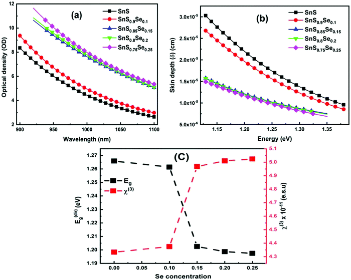 |
| | Fig. 4 (a) Change in the optical density of SnS1−xSex (x = 0, 0.1, 0.15, 0.2, 0.25) thin films, (b) skin depth of SnS1−xSex with energy, and (c) variation of Eg and χ3 with Se doping concentration. | |
3.4.3. Static refractive index, dielectric constant (ε∞), and optical electronegativity (ηOpt).
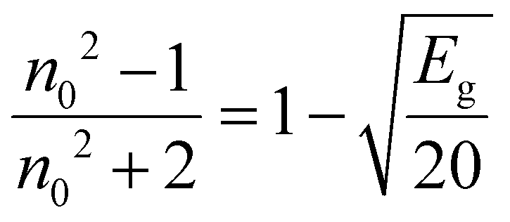
The linear static refractive index (n0) and high-frequency dielectric constant (ε∞) of the sample are related by the equation: ε∞ = n02. The n0 value is calculated by using the Dimitrov and Sakka relation:53| |  | (7) |
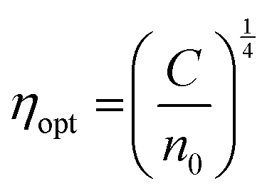
where ‘Eg’ is the bandgap. The calculated values of n0 and ε∞ are presented in Table 2. The calculated data clearly show the increase in the refractive index with the increase of selenium concentration in SnS1−xSex films. Generally, the obtained results are in good agreement with the literature.54 The increase in the refractive index can be attributed to an increase in density by substituting sulphur with a larger amount of selenium.55 From Table 2, it can be observed that the dielectric constant of the lattice increased with the increase in selenium doping. Furthermore, optical electronegativity has a crucial role in determining various physicochemical constants of the material. The parameter ηopt is defined as the ability of atoms or radicals to form ionic bonds due to their tendency to attract electrons. According to Duffy, the optical electronegativity (ηopt) values are determined using the value of n0 as follows:56 , where C is the dimensionless quantity having a value of 25.54. The optical electronegativity values are presented in Table 2. It is observed that the value of ηopt decreased from 1.6874 to 1.6803 as the Se content increased in the SnS1−xSex thin film.57
3.4.4. Nonlinear optical parameters.
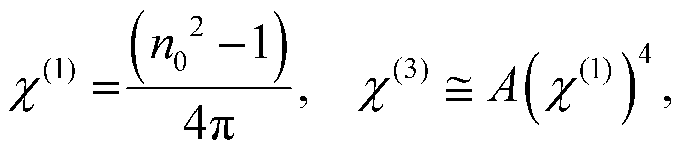
The nonlinear optical response of a material is demonstrated by sufficient intense illumination and also depends on the strength of the electric field, which causes nonlinear effects in the films. The nonlinear behaviour originates from the interaction of the nucleus due to electronic polarizability and its effect on the bond length. The polarization density P(t) is presented by a power series expansion of the total applied optical field:58| | | P(t) = ε0[χ(1)E(t) + χ(2)E(2)(t) + χ(3)E(3)(t)] | (8) |
where ‘E’ refers to the electric field intensity and χ(1) represents the linear behaviour, whereas χ(2) and χ(3) represent the second- and third-order nonlinear susceptibility, respectively. The value of χ(2) is zero for centrosymmetric optically isolated materials.59 Therefore, χ(3) is a superior nonlinear quantity. So the nonlinear susceptibilities χ(1) and χ(3) of the semiconducting material are calculated using Miller's rule as follows:60| |  | (9) |
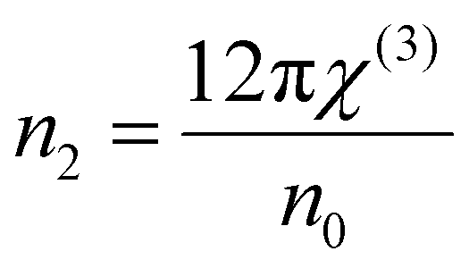
where A = 1.7 × 10⁻¹⁰ (e.s.u.) and n0 refers to the static refractive index at hν → 0. The calculated χ(1) and χ(3) values are presented in Table 2. It is observed that both χ(1) and χ(3) increased with the Se content due to the increase in the n0 value. The increased nonlinear susceptibility makes the material suitable for use in small, compact, and low-power devices for telecommunication purposes.61 The change in Eg and χ(3) with the Se content is shown in Fig. 4(c) which infers an opposite change for the parameters with the Se percentage in ternary SnS1−xSex films. Furthermore, the static refractive index is used to calculate the nonlinear refractive index (n2) by applying the Ticha and Tichy relation with Miller's generalized rule as follows:62 . The calculated values of ‘n2’ are shown in Table 2, which indicates that the value of n2 increased with the Se%, which is for the increase of the refractive index with selenium addition. The high value of the nonlinear refractive index makes the SnS1−xSex films suitable candidates for nonlinear optical applications.
3.5. Theoretical calculations of different physical parameters
3.5.1. Number of constraints and the effective coordination number.
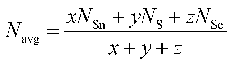
Loffe and Regel demonstrated the bonding characteristics in the nearest neighbor region which shows that the coordination number represents the electronic properties of semiconducting materials.63 The average coordination number (Navg) is calculated by| |  | (10) |
where x, y, and z indicate the atomic % of Sn, S, and Se, respectively, and NSn, NS, and NSe represent the coordination numbers of Sn, S, and Se, having values of 4, 2, and 2, respectively. The corresponding Navg values of the samples are calculated and presented in Table 3.
Table 3 Physical parameters of SnS1−xSex (x = 0, 0.1, 0.15, 0.2, 0.25) thin films
| Sample |
N
avg
|
N
α
|
N
β
|
N = (Nα + Nβ) |

|
V
av
|
L
|
| SnS |
3 |
1.5 |
3 |
4.5 |
64.5 |
5 |
2 |
| SnS0.9Se0.1 |
3 |
1.5 |
3 |
4.5 |
64.12 |
5 |
2 |
| SnS0.85Se0.15 |
3 |
1.5 |
3 |
4.5 |
63.93 |
5 |
2 |
| SnS0.8Se0.2 |
3 |
1.5 |
3 |
4.5 |
63.74 |
5 |
2 |
| SnS0.75Se0.25 |
3 |
1.5 |
3 |
4.5 |
63.55 |
5 |
2 |
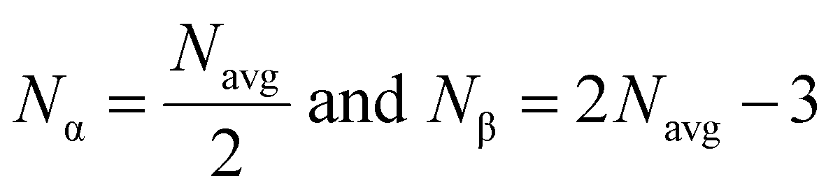
According to Phillips and Thorpe's topological constraint theory, the rigidity of amorphous materials can be calculated by computing the number of constraints experienced by each atom.64 The constraints such as two-body radial band stretching (Nα) and three-body angular constraints (Nβ) are involved in a covalent-like network. These constraint values are calculated by using the average coordination number through the following formula:
| |  | (11) |
Total mechanical constraints per atom were calculated by adding the above two values (
N =
Nα +
Nβ) and are presented in
Table 3.
3.5.2. The average heat of atomization ( ) and lone pair of electrons (L).
The optical bandgap is correlated with the chemical bond energy which is related to the average heat of atomization (Hs). Hs is defined as the quantity of heat energy required to change 1 mol of an element in its standard state at 298 K to the gaseous state. For the compound AxByCz, the average heat of atomization is calculated by65
) and lone pair of electrons (L).
The optical bandgap is correlated with the chemical bond energy which is related to the average heat of atomization (Hs). Hs is defined as the quantity of heat energy required to change 1 mol of an element in its standard state at 298 K to the gaseous state. For the compound AxByCz, the average heat of atomization is calculated by65| |  | (12) |
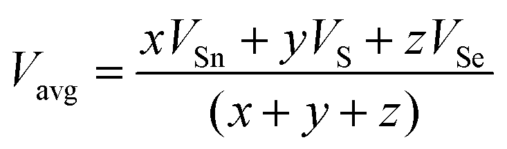
where x, y, and z are the atomic % of Sn, S, and Se, respectively. HSn, HS, and HSe represent the Hs values of Sn, S, and Se (72, 57, and 49.4 kcal g−1 atom), respectively. The average heat of atomization of the samples is calculated and presented in Table 3. From the table, it is observed that the Hs value decreased with the increase of the Se percentage.66 Lone pair electrons are defined as nonbonded electrons present in the valence shell. Although lone pair electrons are nonbonded, these can deform a bond more easily than a bond with no shared electrons. The number of lone pair electrons is calculated through the relation:67L = Vavg − Navg, where Navg is the average coordination number and Vavg is the average valence electrons and expressed as  , where VSn, VS, and VSe are the valence of Sn, S, and Se which are equal to 4, 6, and 6, respectively. The calculated lone pair electrons are listed in Table 3. The cohesive energy of the present system is calculated using heteronuclear and homonuclear bonds based on the chemical bond approach. The heteronuclear bond energy is calculated from the relation:45
| | | C(A–B) = [C(A–A) × C(B–B)]1/2 + 30(χA − χB)2 | (13) |
where χA and χB are the electro-negativity values of the constituent elements Sn, S, and Se, having the values of 1.88, 2.58, and 2.55, respectively. The homonuclear bond energies of Sn–Sn, S–S, and Se–Se are 44.71, 53.8, and 44.04 kcal mol−1, respectively.68 The heteronuclear bond energies of Sn–S, Sn–Se, and S–Se, calculated using the above equation are 63.74, 57.83, and 48.70 kcal mol−1, respectively. The Sn–S bond is expected to form first, as the bond energy of the Sn–S heteropolar bond is more than that of the other bond involved in the present system. After that, Sn–Se and S–S bonds are formed according to the calculated bond energies. Se is doped into the SnS host matrix in the present SnS1−xSex system. Thus, Se atoms prefer to form Sn–Se and S–Se heteropolar bonds. After heteropolar bond formation, there are still unsatisfied Sn and S valences to form homopolar bonds. Thus, there are more homopolar bonds than heteropolar bonds, which leads to more disorder in the system. Due to the presence of group VI elements, there are a large number of lone pair electrons which form the top of the valence band, whereas the antibonding electrons form the bottom of the conduction band. Due to the presence of high-energy lone pair electrons, metal atoms can form dative bonds with group VI elements.68 The localized acceptor states in the gap increased due to the antibonding levels corresponding to the dative bond. Thus, the increased localized state in the gap reduces the optical bandgap.69
4. Conclusion
Ternary SnS1−xSex films were prepared by the thermal evaporation technique at different Se concentrations. This study is focused on changes in their structural and linear/nonlinear optical properties due to Se doping. The XRD spectra of the prepared SnS1−xSex thin films show the crystallinity nature of the pure SnS phase. The crystallinity increased with the increase of Se content due to the formation of new nucleation centers from the dopant atoms. The variation of Se% greatly affects the surface morphology of the film. An increase in the size and density of nanoflake-like structures can be noticed from the FESEM images. The systematic increase in the Se concentration due to doping is confirmed by the EDX analysis. The transmission percentage of the SnS1−xSex films decreased with Se doping, whereas the absorption coefficient and extinction coefficient values increased with Se%. The direct optical bandgap reduced from 1.265 ± 0.001 to 1.197 ± 0.001 eV with Se%. The optical density decreased, whereas the skin depth increased with the Se content. The static refractive index (n0) increased with Se%, further helping to increase the nonlinearity of the films. The nonlinearity parameters like first-order and third-order susceptibility (χ(3)) and the nonlinear refractive index increased with the doping concentration. The average heat of atomization decreased with Se content. These properties make the studied thin films with smaller bandgaps suitable for solar and thermal applications.
Conflicts of interest
There are no conflicts of interest regarding this manuscript.
Acknowledgements
R. Naik thanks the Department of Physics, IISc, Bangalore, for optical, FESEM, and Raman measurements. Dr Naik also thanks ICT-IOCB for the Start-up Research grant.
References
- M. D. Khan, M. Aamir, G. Murtaza, M. A. Malik and N. Revaprasadu, Structural investigations of SnS1−xSex solid solution synthesized from chalcogeno-carboxylate complexes of organo-tin by colloidal and solvent-less routes, Dalton Trans., 2018, 47(30), 10025–10034 RSC.
- R. Fei, W. Li, J. Li and L. Yang, Giant piezoelectricity of monolayer group IV monochalcogenides: SnSe, SnS, GeSe, and GeS, Appl. Phys. Lett., 2015, 107(17), 173104 CrossRef.
- C. J. Liu, S. Y. Tai, S. W. Chou, Y. C. Yu, K. D. Chang, S. Wang, F. S. S. Chien, J. Y. Lin and T. W. Lin, Facile synthesis of MoS2/graphene nanocomposite with high catalytic activity toward triiodide reduction in dye-sensitized solar cells, J. Mater. Chem., 2012, 22(39), 21057–21064 RSC.
- H. Liu, A. T. Neal, Z. Zhu, Z. Luo, X. Xu, D. Tománek and P. D. Ye, Phosphorene: An unexplored 2D semiconductor with a high hole mobility, ACS Nano, 2014, 8(4), 4033–4041 CrossRef CAS PubMed.
- A. Gupta, T. Sakthivel and S. Seal, Recent development in 2D materials beyond graphene, Prog. Mater. Sci., 2015, 73, 44–126 CrossRef CAS.
- A. S. Pawbake, S. R. Jadkar and D. J. Late, High-performance humidity sensor and photodetector based on SnSe nanorods, Mater. Res. Express, 2016, 3(10), 105038 CrossRef.
- W. Shi, M. Gao, J. Wei, J. Gao, C. Fan, E. Ashalley, H. Li, Z. Wang, W. R. Shi, M. X. Gao, J. P. Wei, J. F. Gao, C. W. Fan, E. Ashalley, Z. M. Wang and D. Li, Tin Selenide (SnSe): Growth, properties, and applications, Adv. Sci., 2018, 5(4), 1700602 CrossRef PubMed.
- P. Mandal, B. Show, S. T. Ahmed, D. Banerjee and A. Mondal, Visible-Light Active Electrochemically deposited tin selenide thin films: Synthesis, characterization and photocatalytic activity, J. Mater. Sci.: Mater. Electron., 2020, 31(6), 4708–4718 CrossRef CAS.
- Y. Wang, L. Huang, B. Li, J. Shang, C. Xia, C. Fan, H. X. Deng, Z. Wei and J. Li, Composition-tunable 2D SnSe2(1−x)S2x alloys towards efficient bandgap engineering and high performance (Opto)electronics, J. Mater. Chem. C, 2016, 5(1), 84–90 RSC.
- B. Wang, S. P. Zhong, Z. B. Zhang, Z. Q. Zheng, Y. P. Zhang and H. Zhang, Broadband photodetectors based on 2D Group IVA metal chalcogenides semiconductors, Appl. Mater. Today, 2019, 15, 115–138 CrossRef.
- A. Le Donne, V. Trifiletti and S. Binetti, New earth-abundant thin film solar cells based on chalcogenides, Front. Chem., 2019, 7 Search PubMed.
- R. Guo, X. Wang, Y. Kuang and B. Huang, First-principles study of anisotropic thermoelectric transport properties of IV–VI semiconductor compounds SnSe and SnS, Phys. Rev. B: Condens. Matter Mater. Phys., 2015, 92(11), 115202 CrossRef.
- C. Lu, Y. Zhang, L. Zhang and Q. Yin, Preparation and photoelectrochemical properties of SnS/SnSe and SnSe/SnS bilayer structures fabricated via electrodeposition, Appl. Surf. Sci., 2019, 484, 560–567 CrossRef CAS.
- N. K. Reddy, K. Ramesh, R. Ganesan, K. T. R. Reddy, K. R. Gunasekhar and E. S. R. Gopal, Synthesis and characterisation of co-evaporated tin sulphide thin films, Appl. Phys. A: Mater. Sci. Process., 2006, 83(1), 133–138 CrossRef.
- L. A. Burton, D. Colombara, R. D. Abellon, F. C. Grozema, L. M. Peter, T. J. Savenije, G. Dennler and A. Walsh, Synthesis, characterization, and electronic structure of single-crystal SnS, Sn2S3, and SnS2, Chem. Mater., 2013, 25(24), 4908–4916 CrossRef CAS.
- B. Ghosh, M. Das, P. Banerjee and S. Das, Fabrication and optical properties of SnS thin films by silar method, Appl. Surf. Sci., 2008, 254(20), 6436–6440 CrossRef CAS.
- Z. Tian, C. Guo, M. Zhao, R. Li and J. Xue, Two-dimensional SnS: A phosphorene analogue with strong in-plane electronic anisotropy, ACS Nano, 2017, 11(2), 2219–2226 CrossRef CAS PubMed.
- X. Z. Li, J. Xia, L. Wang, Y. Y. Gu, H. Q. Cheng and X. M. Meng, Layered SnSe nano-plates with excellent in-plane anisotropic properties of Raman spectrum and photo-response, Nanoscale, 2017, 9(38), 14558–14564 RSC.
- H. Tian, C. Fan, G. Liu, S. Yuan, Y. Zhang, M. Wang and E. Li, Ultrafast broadband photodetector based on SnS synthesized by hydrothermal method, Appl. Surf. Sci., 2019, 487, 1043–1048 CrossRef CAS.
- J. Yao, G. Yang, J. Yao and G. Yang, Flexible and high-performance all-2D photodetector for wearable devices, Small, 2018, 14(21), 1704524 CrossRef PubMed.
- J. Xia, D. Zhu, X. Li, L. Wang, L. Tian, J. Li, J. Wang, X. Huang and X. M. Meng, Epitaxy of layered orthorhombic SnS–SnSxSe(1−x) core–shell heterostructures with anisotropic photoresponse, Adv. Funct. Mater., 2016, 26(26), 4673–4679 CrossRef CAS.
- A. Akkari, M. Reghima, C. Guasch and N. Kamoun-Turki, Effect of copper doping on physical properties of nanocrystallized SnS zinc blende thin films grown by chemical bath deposition, J. Mater. Sci., 2012, 47(3), 1365–1371 CrossRef CAS.
- K. S. Kumar, A. G. Manohari, S. Dhanapandian and T. Mahalingam, Physical properties of spray pyrolyzed Ag-doped sns thin films for opto-electronic applications, Mater. Lett., 2014, 131, 167–170 CrossRef CAS.
- H. Kafashan and Z. Balak, Preparation and characterization of electrodeposited SnS:In thin films: Effect of in dopant, Spectrochim. Acta, Part A, 2017, 184, 151–162 CrossRef CAS PubMed.
- W. Gao, Z. Zheng, L. Huang, J. Yao, Y. Zhao, Y. Xiao and J. Li, Self-powered SnS1−xSex alloy/silicon heterojunction photodetectors with high sensitivity in a wide spectral range, ACS Appl. Mater. Interfaces, 2019, 11(43), 40222–40231 CrossRef CAS PubMed.
- K. Santhosh Kumar, C. Manoharan, S. Dhanapandian and A. Gowri Manohari, Effect of Sb dopant on the structural, optical and electrical properties of SnS thin films by spray pyrolysis technique, Spectrochim. Acta, Part A, 2013, 115, 840–844 CrossRef CAS PubMed.
- G. Gordillo, M. Botero and J. S. Oyola, Synthesis and Study of Optical and structural properties of thin films based on new photovoltaic materials, Microelectron. J., 2008, 39(11), 1351–1353 CrossRef CAS.
- J. Yu, C. Y. Xu, Y. Li, F. Zhou, X. S. Chen, P. A. Hu and L. Zhen, Ternary SnS2−xSex alloys nanosheets and nanosheet assemblies with tunable chemical compositions and band gaps for photodetector applications, Sci. Rep., 2015, 5(1), 1–10 CAS.
- W. Gao, Y. Li, J. Guo, M. Ni, M. Liao, H. Mo and J. Li, Narrow-gap physical vapour deposition synthesis of ultrathin SnS1−xSex (0 ≤ x ≤ 1) two-dimensional alloys with unique polarized Raman spectra and high (opto)electronic properties, Nanoscale, 2018, 10(18), 8787–8795 RSC.
- Y. M. Han, J. Zhao, M. Zhou, X. X. Jiang, H. Q. Leng and L. F. Li, Thermoelectric performance of SnS and SnS–SnSe solid solution, J. Mater. Chem. A, 2015, 3(8), 4555–4559 RSC.
- K. Saritha, S. Rasool, K. T. Ramakrishna Reddy, A. M. Saad, M. S. Tivanov, S. E. Tikoto, O. V. Korolik and V. F. Gremenok, Substrate Temperature dependent physical properties of SnS1−xSex thin films, Appl. Phys. A: Mater. Sci. Process., 2019, 125(10), 1–13 CrossRef CAS.
- A. Banotra and N. Padha, Facile growth of SnS and SnS0.40Se0.60 thin films as an absorber layer in the solar cell structure, Mater. Today: Proc., 2020, 26, 3420–3425 CAS.
- D. J. Lim, N. A. Marks and M. R. Rowles, Universal Scherrer equation for graphene fragments, Carbon, 2020, 162, 475–480 CrossRef CAS.
- P. Priyadarshini, S. Das, D. Alagarasan, R. Ganesan, S. Varadharajaperumal and R. Naik, Observation of high nonlinearity in Bi-doped BixIn35−xSe65 thin films with annealing, Sci. Rep., 2021, 11, 21518 CrossRef CAS.
- H. Kafashan, M. Azizieh and Z. Balak, Electrochemical synthesis of nanostructured Se-doped SnS: Effect of Se-dopant on surface characterizations, Appl. Surf. Sci., 2017, 410, 186–195 CrossRef CAS.
- J. Xia, X. Z. Li, X. Huang, N. Mao, D. D. Zhu, L. Wang, H. Xu and X. M. Meng, Physical vapor deposition synthesis of two-dimensional orthorhombic SnS flakes with strong angle/temperature-dependent Raman responses, Nanoscale, 2016, 8(4), 2063–2070 RSC.
- T. S. Reddy and M. C. S. Kumar, Effect of substrate temperature on the physical properties of co-evaporated Sn2S3 thin films, Ceram. Int., 2016, 42(10), 12262–12269 CrossRef CAS.
- H. Zhu, D. Yang, Y. Ji, H. Zhang and X. Shen, Two-dimensional SnS nanosheets fabricated by a novel hydrothermal method, J. Mater. Sci., 2005, 40(3), 591–595 CrossRef CAS.
- P. Pradhan, R. Naik, N. Das and A. K. Panda, Band gap tuning in As40Se53Sb07 thin films by 532 nm laser irradiation: An optical investigation by spectroscopic techniques, Opt. Mater., 2018, 75, 699–709 CrossRef CAS.
- J. Vidal, S. Lany, M. D’Avezac, A. Zunger, A. Zakutayev, J. Francis and J. Tate, Band-structure, optical properties, and defect physics of the photovoltaic semiconductor SnS, Appl. Phys. Lett., 2012, 100(3), 032104 CrossRef.
- R. Naik, A. Aparimita, C. Sripan and R. Ganesan, Structural, linear and non-linear optical properties of annealed and irradiated Ag/Se heterostructure films for optoelectronic applications, Optik, 2019, 194, 162894 CrossRef CAS.
- J. Tauc, Optical properties and electronic structure of amorphous Ge and Si, Mater. Res. Bull., 1968, 3(1), 37–46 CrossRef CAS.
- J. Tauc, Optical properties of amorphous semiconductors, Amorphous Liq. Semicond., 1974, 159–220 CAS.
- S. Wang, X. Lai, B. Du, J. Ma, P. Wang and J. Jian, Synthesis and optical properties of single-crystalline SnS1−xSex nanobelts, Powder Diffr., 2020, 35(4), 276–281 CrossRef CAS.
- Z. A. Alrowaili, M. M. Soraya, T. A. Alsultani, A. Qasem, E. R. Shaaban and M. Ezzeldien, Sn-induced changes in the structure and optical properties of amorphous As–Se–Sn thin films for optical devices, Appl. Phys. A: Mater. Sci. Process., 2021, 127(2), 1–11 CrossRef.
- A. S. Hassanien and A. A. Akl, Effect of Se addition on optical and electrical properties of chalcogenide CdSSe thin films, Superlattices Microstruct., 2016, 89, 153–169 CrossRef CAS.
- r Naik, r Ganesan and K. S. Sangunni, Compositional dependence on the optical properties of amorphous As2−xS3−xSbx thin films, Thin Solid Films, 2010, 518(19), 5437–5441 CrossRef CAS.
- A. S. Hassanien and I. Sharma, Optical properties of quaternary A-Ge15−xSbx Se50 Te35 thermally evaporated thin-films: Refractive index dispersion and single oscillator parameters, Optik, 2020, 200, 163415 CrossRef CAS.
- A. S. Hassanien and A. A. Akl, Influence of composition on optical and dispersion parameters of thermally evaporated non-crystalline Cd50S50−xSex thin films, J. Alloys Compd., 2015, 648, 280–290 CrossRef CAS.
- I. Sharma, Reddy Madara and S. Sharma, P. Study of Tauc Gap, Optical density and penetration depth of vacuum evaporated Pb15Se85−xGex (X = 0, 3, 6 at%) thin films supported by chemical bond approach and physical parameters, Mater. Today: Proc., 2020, 28, 402–407 CAS.
- D. Sahoo, P. Priyadarshini, R. Dandela, D. Alagarasan, R. Ganesan, S. Varadharajaperumal and R. Naik, Investigation of amorphous-crystalline transformation induced optical and electronic properties change in annealed As50Se50 thin films, Opt. Quantum Electron., 2021, 53(4), 1–25 CrossRef.
- N. F. Habubi, S. F. Oboudi and S. S. Chiad, Study of some optical properties of mixed SnO2–CuO thin films, J. Nano- Electron. Phys., 2012, 4, 04008 CAS.
- V. Dimitrov and S. Sakka, Linear and nonlinear optical properties of simple oxides. II, J. Appl. Phys., 1998, 79(3), 1741 CrossRef.
- P. Sharma, K. A. Aly, D. C. Sati and A. Dahshan, Improvement in the linear and nonlinear optical properties of Mn-doped GeSe2 chalcogenide thin films for all optical applications, Appl. Phys. A: Mater. Sci. Process., 2020, 126(3), 1–9 CrossRef.
- I. Sharma and A. S. Hassanien, Effect of Ge-addition on physical and optical properties of chalcogenide Pb10Se90−xGex bulk glasses and thin films, J. Non-Cryst. Solids, 2020, 548, 120326 CrossRef CAS.
- R. R. Reddy, K. Rama Gopal, K. Narasimhulu, L. S. S. Reddy, K. R. Kumar, C. V. K. Reddy and S. N. Ahmed, Correlation between optical electronegativity and refractive index of ternary chalcopyrites, semiconductors, insulators, oxides and alkali halides, Opt. Mater., 2008, 31(2), 209–212 CrossRef CAS.
- A. S. Hassanien, I. Sharma and K. A. Aly, Linear and nonlinear optical studies of thermally evaporated chalcogenide a-Pb–Se–Ge thin films, Phys. B, 2021, 613, 412985 CrossRef CAS.
- E. Sharma, P. B. Barman and P. Sharma, Evaluation of Optical Linear and Non-Linear Parameters of Thermally deposited GeTeSeGa thin films in nir (1–2.6 μm) wavelength range from their transmission spectra, Optik, 2020, 219, 165181 CrossRef CAS.
-
K. Tanaka, Optical nonlinearity in photonic glasses, Springer Handbooks, 2017, p.1 Search PubMed.
- A. S. Hassanien, H. R. Alamri and I. M. El Radaf, Impact of film thickness on optical properties and optoelectrical parameters of novel CuGaGeSe4 thin films synthesized by electron beam deposition, Opt. Quantum Electron., 2020, 52(7), 1–18 CrossRef.
- E. R. Shaaban, M. Mohamed, M. N. Abd-el Salam, A. Y. Abdel-Latief, M. A. Abdel-Rahim and E. S. Yousef, Structural, linear and non-linear optical properties of annealed As47.5Se47.5Ag5 thin films for optoelectronic applications, Opt. Mater., 2018, 86, 318–325 CrossRef CAS.
- I. Sharma, S. K. Tripathi and P. B. Barman, Effect of deposition parameters and semi-empirical relations between non-linear refractive index with linear refractive index and third order susceptibility for a-Ge20Se70−xIn10Bix thin films, J. Appl. Phys., 2011, 110(4), 043108 CrossRef.
- A. A. Othman, K. A. Aly and A. M. Abousehly, Effect of Te additions on the optical properties of (As–Sb–Se) thin films, Thin Solid Films, 2007, 515(7–8), 3507–3512 CrossRef CAS.
- M. Behera, R. Naik, C. Sripan, R. Ganesan and N. C. Mishra, Influence of Bi content on linear and nonlinear optical properties of As40Se60−xBix chalcogenide thin films, Curr. Appl. Phys., 2019, 19(8), 884–893 CrossRef.
- A. H. Ammar, A. M. Farid and S. S. Fouad, Optical and other physical characteristics of amorphous Ge–Se–Ag alloys, Phys. B, 2001, 307(1–4), 64–71 CrossRef CAS.
- S. Das, P. Priyadarshini, D. Alagarasan, S. Vardhrajperumal, R. Ganesan and R. Naik, Role of tellurium addition on the linear and non-linear optical, structural, morphological properties of Ag60−xSe40Tex thin films for nonlinear applications, J. Am. Ceram. Soc., 2022, 105, 3469–3484 CrossRef CAS.
- E. R. Shaaban and I. B. I. Tomsah, The effect of Sb content on glass-forming ability, the thermal stability, and crystallization of Ge–Se chalcogenide glass, J. Therm. Anal. Calorim., 2011, 105(1), 191–198 CrossRef CAS.
- R. Naik and R. Ganesan, Effect of compositional variations on the optical properties of SbxSe60−xS40 thin films, Thin Solid Films, 2015, 579, 95–102 CrossRef CAS.
- X. Feng, W. J. Bresser and P. Boolchand, Direct evidence for stiffness threshold in chalcogenide glasses, Phys. Rev. Lett., 1997, 78(23), 4422 CrossRef CAS.
|
| This journal is © The Royal Society of Chemistry 2022 |
Click here to see how this site uses Cookies. View our privacy policy here. 
 Open Access Article
 This Open Access Article is licensed under a Creative Commons Attribution-Non Commercial 3.0 Unported Licence
 *a
*a
 . The variation of ‘δ’ with ‘hν’ is shown in Fig. 4(b). It is observed that ‘δ’ decreased with the increase of ‘hν’ as well as with the Se content. The increase in the Se content leads to a decrease in the transparency of the film.

 , where C is the dimensionless quantity having a value of 25.54. The optical electronegativity values are presented in Table 2. It is observed that the value of ηopt decreased from 1.6874 to 1.6803 as the Se content increased in the SnS1−xSex thin film.57
 . The calculated values of ‘n2’ are shown in Table 2, which indicates that the value of n2 increased with the Se%, which is for the increase of the refractive index with selenium addition. The high value of the nonlinear refractive index makes the SnS1−xSex films suitable candidates for nonlinear optical applications.

 ) and lone pair of electrons (L).
The optical bandgap is correlated with the chemical bond energy which is related to the average heat of atomization (Hs). Hs is defined as the quantity of heat energy required to change 1 mol of an element in its standard state at 298 K to the gaseous state. For the compound AxByCz, the average heat of atomization is calculated by65
) and lone pair of electrons (L).
The optical bandgap is correlated with the chemical bond energy which is related to the average heat of atomization (Hs). Hs is defined as the quantity of heat energy required to change 1 mol of an element in its standard state at 298 K to the gaseous state. For the compound AxByCz, the average heat of atomization is calculated by65
 , where VSn, VS, and VSe are the valence of Sn, S, and Se which are equal to 4, 6, and 6, respectively. The calculated lone pair electrons are listed in Table 3. The cohesive energy of the present system is calculated using heteronuclear and homonuclear bonds based on the chemical bond approach. The heteronuclear bond energy is calculated from the relation:45