DOI:
10.1039/D2MA00087C
(Paper)
Mater. Adv., 2022,
3, 3897-3905
First-principles study of the defect-activity and optical properties of FAPbCl3†
Received
25th January 2022
, Accepted 24th March 2022
First published on 1st April 2022
Abstract
With promising solar cell applications, organic–inorganic lead halide perovskites belong to a novel and rapidly developing class of semiconducting materials. Unlike its well-investigated iodide counterparts, formamidinium lead chloride (FAPbCl3) is a much less studied perovskite that shows superior stability and surprisingly high selectivity and sensitivity towards certain gas analytes. The origin of the sensing ability of this perovskite material can be traced to its high defect tolerance and the existence of some defects which act as the “lock” to a certain gas analyte's “key”. In this work, we deepen the understanding of this proven perovskite sensor through first-principles computational study of its defect formation energies, charge transition energies, and optical properties. These studies are done with the widely used GGA exchange–correlation functional PBE and the newer meta-GGA functional SCAN, both incorporating the Grimme's D3 dispersion correction. Additionally, we also consider experimental conditions and the effect of temperature on electron screening in the simulations, which demonstrates that screening is particularly important when considering high oxidation states of the defects. We also note the importance of antisites in the Fermi Pinning as well as the importance of FA disorder, which are previously unreported insights.
Introduction
Ever since their discovery, organic–inorganic hybrid perovskites (OIHPs) of formula ABX3 (A = methylammonium (MA), formamidinium (FA); B = Sn, Pb; X = Cl, Br, I) have generated significant interest as photovoltaic (PV) materials. This is mainly due to their remarkable photovoltaic efficiency (PVE) which has climbed to 25.5% as of the time of writing.1 This remarkable PVE is attributable to severable favorable properties including high carrier mobility,2 long carrier diffusion lengths,3 low recombination rate4 and high defect tolerance.5–7 Another factor which is favorable towards their widespread adoption is their relatively simple solution-based manufacturing process.8–11 Iodine-based perovskite materials – shown experimentally to be direct band-gap semiconductors12 – have an abnormally high absorption coefficient in the visible light range which allows the materials to function as a very thin absorbing layer in photovoltaic cells, decreasing efficiency losses which occur due to electron–hole recombination.13,14 The ability to vary band-gap by changing the composition of the metal halide perovskites makes them prime candidates for multi-junction perovskites, possibly enabling overall photon absorption exceeding the Shockley–Queisser limit.15 The primary drawback which inhibits the commercial applications of OIHPs is their low operation lifetime. This is due to the observed degradation of the PVE after a few thousand hours of use regardless of experimental conditions.16 The sources of the degradation are varied, including detrimental interactions with environmental moisture17 as well as sources which are seen even in inert settings such as thermal degradation,18 photodegradation19,20 and ion migration.21,22 In many cases the culprit is suspected to be the migration of the halide vacancy formed from the X site, which is the case for the popular methyl ammonium lead iodide (MAPbI3).23 Despite the challenges remaining for applications of this relatively new material class, its promising outlook necessitates better understanding of all of the phenomena affecting PVE, from surface to bulk.
One of the most influential factors on the properties of semiconductors in general are the types and concentrations of various defects present.24 For example, the majority charge carrier identity of the well-studied case of MAPbI3 is influenced by varying chemical potential of the growing environment due to the particulars of point defect physics.25 Point defects in the bulk of the material are a major driver, with the lifetime, mobility and recombination rate of charge carriers all affected by them, as well as the doping limit of the material. According to Shockley-Read-Hall theory, so-called “deep” or “trap” defects located deep in the band gap can lower the PVE by allowing increased nonradiative recombination rate of charge carriers via balancing the ease of hole and electron trapping from the respective band edges.26,27 On the other hand, “shallow” defects near the band edges with energies of the order of the thermal energy of the lattice can facilitate carrier generation and are likely to emit electrons or holes before recombination can occur. Shallow defects tend to be self-regulating in a process known as Fermi level pinning, in which a low formation energy donor–acceptor pair maintains the Fermi level by forming more of the appropriate donor or acceptor defect as the Fermi energy varies from the pinned level. This phenomenon is a likely contributor to the high defect-tolerance of OIHPs.5,23 It is necessary to have a detailed understanding of the nature of point defects and the relevance to the electronic structure of a given OIHP material.
Although much attention has been placed on their use in photovoltaics, OIHPs also find applications in fields such as organic–inorganic light-emitting diodes,28,29 photodetectors2,9,30 and lasers.8,31 The same instability in the presence of foreign species or when subjected to illumination, which is a drawback for PVE, can actually function as a strength for these alternate applications.17,19,20 In addition to these optoelectronic applications, metal-halide perovskites are also investigated experimentally as sensors for their readily tunable optical and chemical properties such as band-gap and emission intensity/wavelength.32 For example, Gu et al. demonstrated the feasibility of organometal halide perovskite nanowires arrays as image sensing systems33 and another group utilized the known sensitivity of ionic perovskite crystals to water to manufacture reusable humidity sensors which were able to out-perform commercial hygrometers.15 Zhuang et al. achieved good response times and high selectivity towards detection of NO2 and acetone using an organometal halide perovskite doped with SCN− anions as the sensing material in an electrochemical sensor.34
Recently, we published a work reporting on a FAPbCl3-based sensor which shows a highly sensitive and selective signal for ammonia while being insensitive towards most other gasses regardless of polarity, such as CO, MeOH, and H2S, which often confound ammonia sensing efforts through signal obfuscation.35 Although evidence has been provided to substantiate the proposed lock-and-key healing mechanism regarding the VCl defect, no comprehensive defect analysis was performed.7 The present work endeavours to increase our understanding of this relatively unexplored perovskite and its sensing mechanism of applications. First principles-based density functional theory (DFT) allows for direct probing of material properties which are difficult to experimentally observe, such as the formation energies of the various potential defects from the pristine crystal cell.36,37 For this reason, DFT is a standard technique for investigating the nature of these critical defects and the effects that they have on the electronic structure of the OIHPs and is a critical tool in the realization of intelligently engineered materials. In this study, we use DFT calculations to elucidate the defects in FAPbCl3 that control the Fermi pinning behavior, which self-regulates the Fermi level of the material by forming charge carriers thus mitigating deviations from the pinned Fermi level. Structural optimizations are carried out using a widely used generalized gradient approximation (GGA) functional. Subsequently, single point energy and property evaluation are done using a more recently (2015) introduced meta-GGA functional, namely the Strongly Constrained and Appropriately Normed (SCAN) functional of Sun et al.38 The latter functional is particularly useful for thermodynamic calculations since it was recently demonstrated that this functional is better than GGA or local density approximation (LDA) functionals at predicting the lattice parameters and formation enthalpies of CsPbI3 phases; it also did not show ferroelectric instability in the phonon spectra, unlike LDA which erroneously reported the material as ferroelectric.39 SCAN has also been shown to yield reliable results for semiconductor bandgaps comparable to the widely used HSE hybrid functional40 but at reduced computational cost.41–44 By analyzing the formation energies of the various electron donating and accepting defects as a function of the Fermi energy, we found antisite defects, which are not previously studied, are in fact thermodynamically quite significant.
Theoretical methods
For all of the DFT calculations performed, we utilized the Vienna Ab Initio Simulation Package (VASP).45 All structural optimizations made use of the Perdew–Burke–Ernzerhof (PBE)46 generalized gradient approximation (GGA) functional and projector augmented-wave (PAW) pseudopotentials.47 The Grimme D3 dispersion corrections were used in all calculations.48 The cubic FAPbCl3 unit cell was optimized and then used to build a 3 × 3 × 3 supercell. Since each formamidinium cation of the supercell was aligned in the same (100) direction, we classify this as the “ordered” phase. This ordered phase was first optimized with a single gamma point and then, 3 × 3 × 3 sampling of the k-space was used. Each defect considered was introduced to this cell. Finally, single-point calculations with SCAN38,49 meta-GGA functional were performed – incorporating the D3 dispersion corrections – at the PBE+D3 optimized geometries in order to compare its results with that of the PBE functionals.
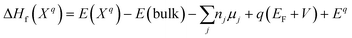
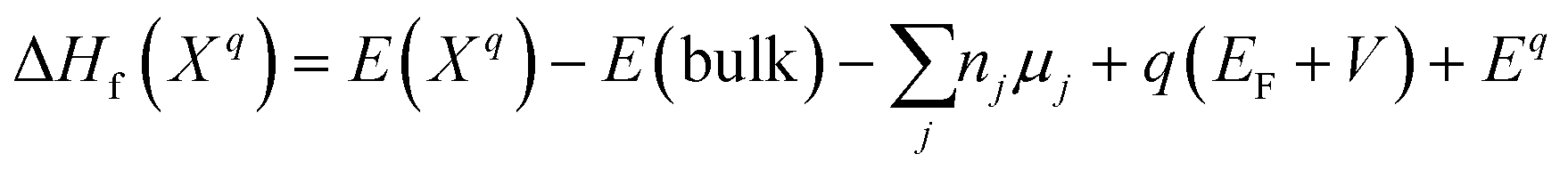
Defect energetics can be studied by introducing the defect into a supercell and comparing the energy of that cell with the pure case. The defect formation energies (DFEs) are calculated as:
| |  | (1) |
where
E(
Xq) is the energy of the ordered supercell with the defect
X with
q oxidation state;
E(bulk) is the energy of the ordered, pristine crystal;
n and
μ refer to the number and chemical potential of the species removed from or added to the pristine crystal to form the defect
X; the fourth term pertains to the energy required to add/remove an electron:
q is the charge of the defect,
EF is the Fermi level relative to the valence band maximum (VBM) of the pure crystal,
V is the energy at the VBM; the final term is the Makov–Payne (electrostatic screening) correction sans multipole contribution (which scales according to L
−3 and so is justifiably negligible), with the monopole portion shown in
eqn (2) below.
| |  | (2) |
where
q is the charge of the defect,
α is the Madelung constant,
ε is the dielectric constant, and
L is the characteristic length of the cell (taken to be the geometric average of the lattice constants). The dielectric constant was calculated to be 4 at 0 K but is found to be 28 at 298 K in experimental conditions which implies a very significant temperature-dependent increase in coulombic screening. DFE plots were made for both temperatures to examine how the electrostatic correction influences the DFE according to temperature. In addition to the DFE's as a function of
EF, coupling with the band edges must also be considered as the VBM and conduction band minimum (CBM) act as an electron acceptor and donor, respectively. The methodology for this has been described by Yang
et al.37 and so is omitted here.
For eqn (1), the limits of the potentials must be established. This is done by imposing the bulk potentials of the various species in the ABX3 formulations as energetic ceilings (otherwise the bulk material would be formed).
| | | μFA + μPb + 3μCl = ΔHf(FAPbCl3) | (3) |
| | | μPb + 2μCl = ΔHf(PbCl2) | (4) |
The heat of formation for
eqn (3)–(5) are calculated through the standard method of the difference between the material being formed and the component ions.
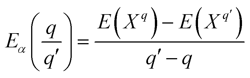
Finally, the transition energies, also referred to as thermodynamic ionization levels, were calculated as:
| |  | (6) |
where

is the transition energy of defect
X with charge
q to charge state
q′.
Results and discussion
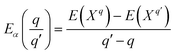
Shown below in Table 1 are the results from the thermodynamic analysis for each DFT functional. The resulting phase diagram for PBE + D3 is shown in Fig. 1(a), with only a narrow range of stability for FAPbCl3. However, the range is notably wider for SCAN + D3 as seen in Fig. 1(b). It was previously noted that disordering the FA molecules also widens the range.35 It is from this range of stability that the three limiting cases are chosen (Fig. 1(a)): the green dot representing the Cl-rich case, the purple the intermediate, and the blue the Pb-rich case. The case of a perovskite synthesis with a Cl-rich solution drives the μCl to 0, with the Pb-rich situation being analogous for μPb.
Table 1 Enthalpies of formation (in eV) for forming the boundaries on the phase diagram according to eqn (3)–(5)
| DFT Functional |
ΔHf(FAPbCl3) |
ΔHf(PbCl2) |
ΔHf(FACl) |
| PBE + D3 |
−6.13 |
−3.44 |
−2.78 |
| SCAN + D3 |
−6.25 |
−3.44 |
−2.95 |
 |
| | Fig. 1 The calculated phase diagram of FA-Pb-Cl systems. (a) with PBE + D3 functional. (b) with SCAN + D3 functional. The three symbols in (a) represent the Cl-rich (green dot at μCl = 0 eV), Pb-rich (blue dot at μPb = 0 eV), and the intermediate case (purple dot), respectively. | |
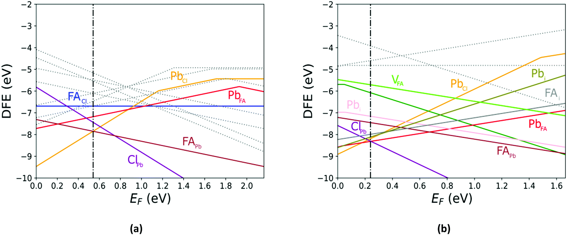
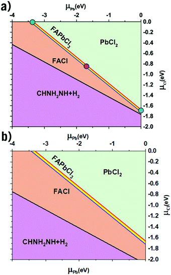
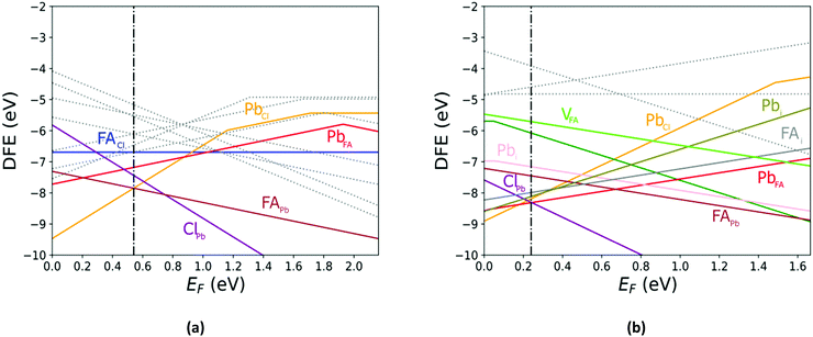
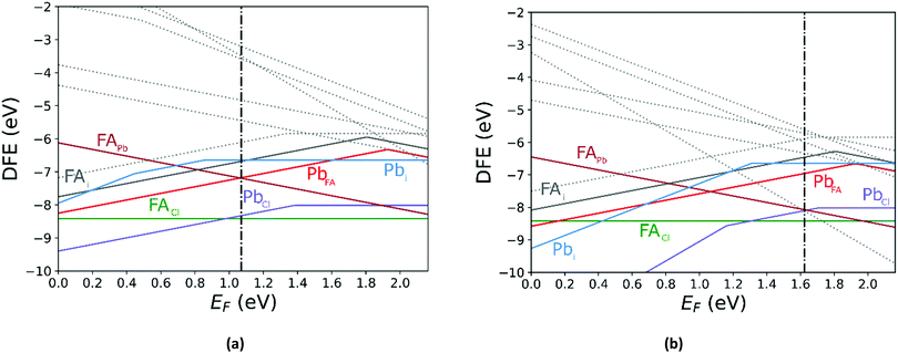
The defect energy plots and defect transition energies in Fig. 2 and 3 respectively highlight the differences between the results of the PBE + D3 and SCAN + D3 calculations. The vertical dashed line in Fig. 2 indicates the value of the Fermi level caused by the defect pair that controls the pinning. The two functionals result in broadly similar DFE function shapes, although the point at which the lowest energy DFE charge state for each defect transitions varies significantly, as does the magnitude of the DFE. The case for PBE + D3 with intermediate component ion potentials [purple dot in Fig. 1(a)] at 0 K is shown in Fig. S1(a) in the ESI.† As can be seen, the contributions of the commonly studied vacancies and interstitials are overshadowed by the contributions of the lower formation energy anti-site defects. This more negative DFE indicates that the formation of the defect is more energetically favorable, and thus that the defect plays a more important role in the properties of the material due to the Arrhenius-type relationship between the DFE and the defect concentration.37 The vertical black line highlights the intersection point of the defect pair which dictates the pinning behavior, here being the PbFA cationic defect and the FAPb anionic defect. The induced pinning is at 0.23 eV above the VBM, which indicates that a p-type semiconductor will be formed under stoichiometric synthesis conditions. Fig. S1(b) (ESI†) shows the case of SCAN + D3 with intermediate potentials at 0 K. The same pair of defects is found to be important to the pinning in this case, and the pinned Fermi level is still nearer to the VBM than the CBM, again indicating p-type behavior. We summarize the Fermi pinning behavior for all cases considered in Table 2. Generally, SCAN + D3 and PBE + D3 often predict the same qualitative results regarding p-type vs. n-type character, but in some cases differ significantly in the depth in the band gap of the pinned Fermi level. A notable exception is the Pb-rich case, for which the Makov-Payne (MP) correction is quite important due to the prominent role played by the highly charged PbCl and ClPb defects. Here, the large magnitude of the charges of these defects increases the contribution of the correction to the DFE viaeqn (2). This large difference in pinned Fermi level highlights the importance of seemingly minute variations in the calculated thermodynamics of the defects, demonstrating that the accuracy afforded by the better approximation of the exchange–correlation energy by SCAN + D3 is crucial to prediction of the Fermi level pinning behavior. Fig. 3 contains the intersection state plots at 0 K for both functionals with defects labelled using the Kröger–Vink notation.50 PBE + D3 resulted in a band gap of 2.163 eV versus a much lower 1.665 eV for SCAN + D3. The cationic defects are listed first followed by the anionic defects. When comparing the defect transition energies, we note that the two functionals give relatively similar results (Fig. 3). Generally, the intersections are quite similar in ordering and energy; however, PBE + D3 has fewer intersections between higher oxidation states than SCAN + D3. Notably, PBE + D3 predicts deep traps for PbFA, FAi, Pbi, and VCl while SCAN + D3 does not share this result for VCl, mainly due to the reduction in predicted lowest unoccupied molecular orbital energy level; however, PbFA and FAi are both relatively insignificant due to kinetic hindrance caused by a two-hole (−/+) transition. For PbFA, FAi, and Pbi the traps are shallower due to being shifted towards the conduction band. Another significant difference seen in the anionic defects is that PBE + D3 predicted transitions just inside of the conduction band while SCAN + D3 predicts relatively shallow traps within the gap, e.g. Cli's (1-/0) transition. Finally, ClFA and PbCl are both predicted by SCAN + D3 to have a pair of twin transition levels, whereas PBE + D3 only predicted one of the intersections occurring; the ClFA pair of transitions is quite near the center of the band gap, indicating that it may also act as a deep trap. Overall, a significant driver in the difference in trap types predicted by the two methods is the band gap difference. These results indicate that while the origin of deep trap levels may be in many cases due to the interstitial and vacancy defects normally considered, the antisite defects are sometimes potential deep traps and are also found to be significant in determining the pinned Fermi level and thus the concentrations of the deep trap defects.
 |
| | Fig. 2 The calculated defect formation energy (DFE) as a function of the Fermi level for FAPbCl3. (a) PBE + D3 with intermediate potentials at 300 K. (b) SCAN + D3 with intermediate potentials at 300 K. The vertical dashed line indicates the value of the Fermi level caused by the defect pair that controls the pinning. | |
 |
| | Fig. 3 The calculated transition energy levels of vacancy, interstitial and antisite defects of FAPbCl3 of (a) PBE + D3 and (b) SCAN+ D3. The red field represents the valence band while the blue represents the conduction band. The notation is ordered as acceptor/donor with charge states. The cationic defects are listed first followed by the anionic defects. | |
Table 2 The Fermi Pinning Energies (FPE) for the 0 and 300 K Cl-Rich, Intermediate, and Pb-Rich cases from PBE + D3 and SCAN + D3 functionals. These FPEs correspond to the vertical black lines on the DFE figures. The middle of the band gap for the cases of PBE + D3 and SCAN + D3 are at 1.08 eV and 0.83 eV, respectively
|
|
Cl-Rich |
Intermediate |
Pb-Rich |
| 0 K |
300 K |
0 K |
300 K |
0 K |
300 K |
| PBE + D3 FPE (eV) |
0.22 |
0.22 |
0.21 |
0.54 |
1.07 |
1.63 |
| SCAN+D3 FPE (eV) |
0.68 |
0.12 |
0.67 |
0.24 |
1.53 |
1.10 |
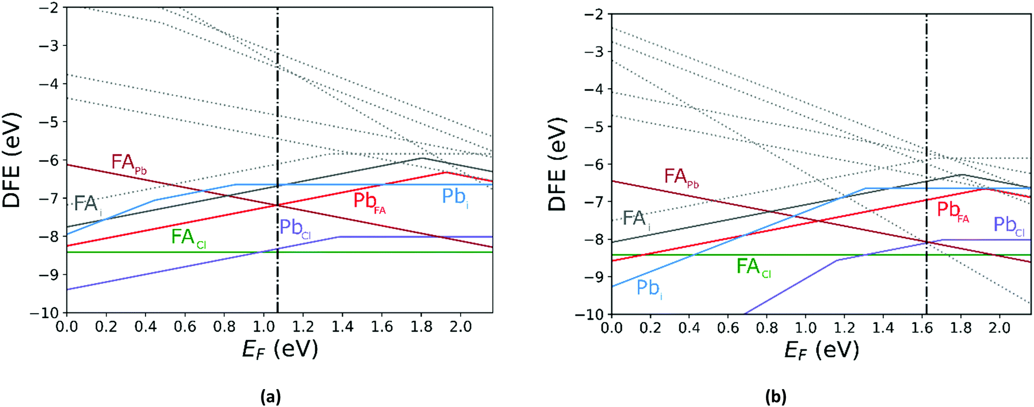
Comparing the Cl-rich case of Fig. S2 in ESI† and Pb-rich case of Fig. 4(a) highlights the importance of experimental synthesis conditions. Merely changing the potentials of the constituent ions results in the pinned Fermi level shifting from 0.22 eV to 1.07 eV at 0 K and thereby lower carrier concentrations due to the deep location of the Fermi level in the Pb-rich case.
 |
| | Fig. 4 The calculated defect formation energy (DFE) as a function of the Fermi level for FAPbCl3 using PBE + D3 with Pb-rich potentials for (a) 0 K and (b) 300 K. The vertical dashed line indicates the value of the Fermi level caused by the defect pair that controls the pinning. | |
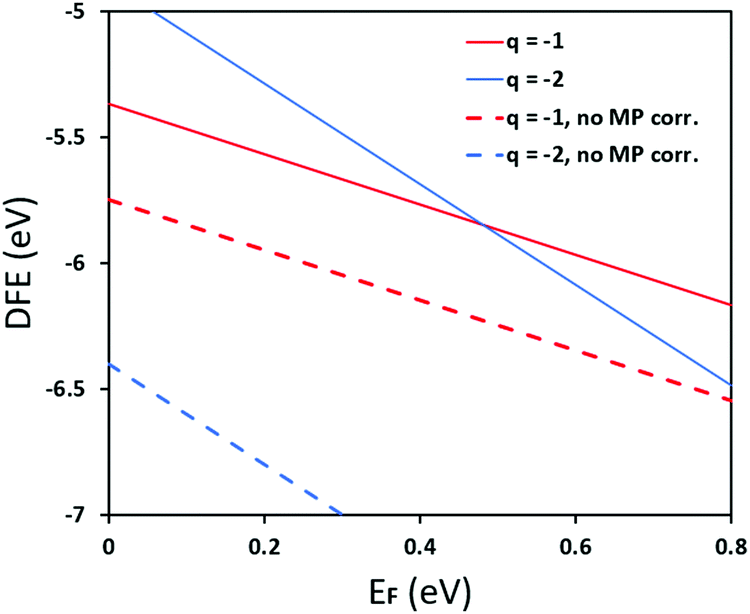
In Fig. 5 we further illustrate the importance of including the Makov–Payne correction by showing the DFE of the VPb2− and VPb1− with and without the correction included. It should be noted that each of the terms within eqn (2) do not vary between PBE + D3 and SCAN + D3, so the MP correction for a given defect and charge state at a particular temperature is the same for both. While the case where the correction is omitted shows the two DFE series which never intersect within the band thus leaving the −2 series lower in energy, the inclusion of the correction correctly shows a transition within the band to the −1 oxidation state. Introducing the effect of temperature via the dielectric constant in the MP correction and comparing Fig. 4(a) with Fig. 4(b), the correction again is shown to be important, this time via its mitigation with increasing temperature due to a significant increase in the dielectric constant, which is inversely proportional to the MP correction's magnitude. The shifting of the PbCl defect's transition energy levels compared to the 0 K case in Fig. 4(a) results in n-type pinning induced by its interaction with the FAPb defect.
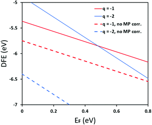 |
| | Fig. 5 Pb vacancy for the case of PBE + D3 with Cl-rich potentials at 0 K, with and without the Makov-Payne correction. The inclusion of the Makov–Payne correction, indicated via solid lines, predicts a thermodynamic ionization level from −1 to −2 around 0.51 eV whereas excluding the correction predicts no intersection within the entire bandgap. This illustrates the importance of including the electrostatic screening correction, even if only for the monopole correction. | |
The material is best compared to FAPbI3. The most immediate difference when comparing FAPbCl3 to FAPbI3 is that the latter is not stable in the cubic perovskite phase at room temperature. Meanwhile, FAPbCl3 is experimentally known to be stable in the α phase.35 This can be explained by the difference in the Goldschmidt tolerance factor t:
| | 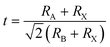 | (7) |
where each
R corresponds to ionic radii of the corresponding perovskite formula ABX
3. The tolerance factor of FAPbI
3 is slightly above 1.0 meaning that it is at the very borderline of the perovskite phase stability range 0.8–1.0.
51 Since Chlorine is considerably smaller than iodine this decreases the factor to 0.94.
52
The tolerance factor can be thought of as a measure of strain inside of the perovskite unit cell. A proposed reason for the ease with which iodine vacancies form in FAPbI3 is that such point defects release strain,53 the resulting interstitial iodides can then have an undesirable tendency to rotate the PbI6 octahedra, which is what causes the phase instability.54 Since FAPbCl3 is not strained it does not stabilize such vacancies.
However, it's notable that the antisites we have calculated appear to be abnormally stable when compared to other perovskite materials. If, in the case of eqn (1) we replace E(bulk) with the value of the disordered material then we observe an upward shift of the DFE values of about 8 eV with nearly none of the defects retaining a negative DFE. However, if the material was to be considered totally disordered this would imply a very low concentration of vacancy defects. This would imply that it is not a good lock-and-key optical sensor, which is contrary to our previous work.35 There we observed the sensitivity originating from the localized disorder of the cubic phase, rather than the disorder of the whole material. As such, we believe that further experimental guidance is needed to fully understand the point defect concentrations. Since disorder so strongly affect the DFE's, it's likely that the real material is in a range between full order and full disorder. Regardless of this issue, it is clear that this perovskite material is very unique in its strong preference towards antisites.
Strong absorption peaks are shown in the UV-Vis optical spectrum of this FAPbCl3 perovskite material.35 To further investigate the impact of defects on the optical properties of FAPbCl3, spin-orbital coupling (SOC), which is known to be important when calculating optoelectronic properties of heavy elements,55 is included in the calculations derived in this section. This was investigated by obtaining the frequency-dependent dielectric matrix in the long wavelength limit with a sum over states approach.56 The procedure is available in the ESI,† as a more complete description is available in our previously published papers.57–60 With the real and imaginary portions of the dielectric constant calculated, it is straightforward to evaluate optical absorption, α, for a particular wavelength, λ:
| | 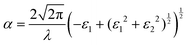 | (8) |
The results of the optoelectronic calculations with SOC included for the cases of PBE + D3 and SCAN + D3 with intermediate potentials at 300 K are shown in
Fig. 6. Other optical properties, such as dielectric tensor, optical conductivity, extinction coefficient, index of refraction and reflectivity for both PBE + D3 and SCAN + D3 are presented in Fig. S3–S6 in ESI.
† The two pinning defects for this case, FA
Pb1− and FA
Cl3+, are shown alongside the absorption spectrum of the pristine supercell for comparison. Comparing the result of the optical calculations with the experimental absorption spectrum reproduced from Parfenov
et al.'s
Fig. 2(d),
35 the two plots share a pair of characteristic peaks near 300 nm. As demonstrated in
Fig. 6 and Fig. S3–S7 (ESI
†), the calculations results show the peaks shifted to lower wavelengths as compared to experiment, but the interval within the peaks is comparable. Note that the magnitude scaling of the experimental data relative to the calculation results is arbitrary. As is apparent, both PBE + D3 and SCAN + D3 can predict the two adsorption peaks appeared in the UV-Vis optical spectrum (
Fig. 6). However, compared to the experimental peak locations (309 nm and 399 nm), peak position shifting exists in our simulation results. For PBE + D3, it seems that there is a better prediction of the first peak in visible light range (399 nm) while the SCAN + D3 identifies the second one (309 nm) in UV light range more accurately. The simulation predictions also give a narrower wavelength difference between the two absorption peaks, where SCAN + D3 seems to work slightly better (Δ
λPBE+D3 = 38 nm; Δ
λSCAN+D3 = 47 nm). The presence of either types of defects reduces the absorption of light, with the effect being less for Pb
Cl3+. Both types of defects also lead to further blue shift of those absorption peaks, which is less affected by the FA
Pb1− defects. Similar trends are also observed with other optical property calculations (Fig. S3–S6, ESI
†), with PBE + D3 results showing differences for cases with/without defects in a longer wavelength range than the SCAN + D3 predictions. These results confirm the sensitivity of this type of perovskites to certain wavelength of light and the impact of defects on its optical properties.
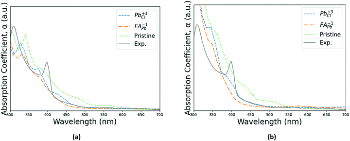 |
| | Fig. 6 Absorption spectrums of the pristine perovskite with the two pinning defects for (a) PBE + D3 and (b) SCAN + D3 with intermediate potential at 300 K. Calculated spectra are compared with experimental spectrum from Parfenov et al.35Fig. 2(d) in shape and characteristic peak gap, although being shifted to lower wavelengths. Note that the experimental data's scaling relative to the other three series is arbitrary for both PBE + D3 and SCAN + D3. | |
Finally, to understand the role of order and disorder in the material we plotted the top 3 occupied orbitals (HOMO) and top 3 unoccupied orbitals (LUMO) (Fig. 7), we took a weighted sample of k points for these plots. Beneath these plots we also plot the density of states (DOS). The ordered phase of the material is quite ordinary for a perovskite material – the valence band is mostly represented by Cl(p) while the conduction band is mostly represented by Pb(p). We can see; however, that the disordered phase of the material is highly unusual in that the random rotations of the FA creates traps inside of the band gap. Both acceptor and donor deep defects are visible. The HOMO and LUMO indicate that these defects are localized to the formamidinium ions both in the HOMO and the LUMO. This highly unusual result implies that the formamidinium orientation will strongly influence photovoltaic properties of the material. Previously, we proposed that ammonia will temporarily heal the chloride vacancy which would temporarily restore the material's electrical conductivity; however, we can also now propose that the healing also temporarily lowers the disorder of the material.
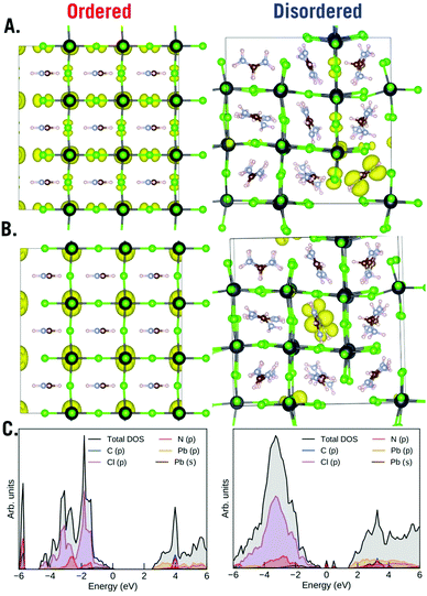 |
| | Fig. 7 SCAN + D3 plots of (A) HOMO, (B) LUMO and (C) DOS of the ordered and disordered phases of cubic FAPbCl3. | |
Conclusions
In this work we used first-principles density functional theory to investigate the defect formation energetics of FAPbCl3. Using a generalized gradient approximation (GGA) functional, a unit cell was relaxed to an energy-minimized geometry before being expanded to a pristine supercell. Next, the various potential vacancy, interstitial, and antisite defects were constructed from this supercell and all were relaxed. These GGA-optimized structures were then considered using a new meta-GGA functional to compare its output. The defect formation energetics were calculated for the thermodynamically derived chemical potential extrema, as well as at temperatures of 0 K and 300 K. Antisites, often neglected in prior literature, were found to in some cases be thermodynamically relevant both to the pinning behavior and as deep traps which influence optoelectronic properties. The calculated optical properties of FAPbCl3 are comparable with experimental findings. Overall, both FAPb1− and FAPb3+ defects reduce optical absorption in the visible light range. The results elucidated the effect that the synthesis environment and temperature can have on the Fermi level pinning behavior of the material, which is consequential to the electronic properties of the material and consequently its performance as a sensor. Our analysis of the electronic structure of the material indicated the surprising importance of ordering in the material, we showed that even the pure material can acquire deep traps from the mere rotation of the FA molecules in the lattice. As such, while the defect energetics and Fermi level pinning are difficult somewhat difficult to analyze experimentally, we hope that this paper aids in establishing the working knowledge of the physics that affect the performance of real-world devices and inspires further investigation.
Conflicts of interest
There are no conflicts to declare.
Acknowledgements
S. N. thanks the Louisiana Board of Regents (LBR) for supporting his research through the LBR Graduate Fellowship. S. N. and L. G. thank the Louisiana Optical Network Infrastructure (LONI) for the computational infrastructure used to complete this project. L. G. Gutsev acknowledges the Russian Science Foundation Grant No. 21-73-00080 for financially supporting this work.
References
- Best Research-Cell Efficiency Chart | Photovoltaic Research | NREL, https://www.nrel.gov/pv/cell-efficiency.html (accessed 15 June 2021).
- M. I. Saidaminov, V. Adinolfi, R. Comin, A. L. Abdelhady, W. Peng, I. Dursun, M. Yuan, S. Hoogland, E. H. Sargent and O. M. Bakr, Nat. Commun., 2015, 6, 1–7 Search PubMed.
- S. D. Stranks, G. E. Eperon, G. Grancini, C. Menelaou, M. J. P. Alcocer, T. Leijtens, L. M. Herz, A. Petrozza and H. J. Snaith, Science, 2013, 342, 341–344 CrossRef CAS PubMed.
- S. D. Stranks, V. M. Burlakov, T. Leijtens, J. M. Ball, A. Goriely and H. J. Snaith, Phys. Rev. Appl., 2014, 2, 34007 CrossRef CAS.
- D. Meggiolaro, S. G. Motti, E. Mosconi, A. J. Barker, J. Ball, C. Andrea Riccardo Perini, F. Deschler, A. Petrozza and F. De Angelis, Energy Environ. Sci., 2018, 11, 702–713 RSC.
- W. Li, R. Long, J. Tang and O. V. Prezhdo, J. Phys. Chem. Lett., 2019, 10, 3788–3804 CrossRef CAS PubMed.
- S. G. Motti, D. Meggiolaro, S. Martani, R. Sorrentino, A. J. Barker, F. De Angelis and A. Petrozza, Adv. Mater., 2019, 31, 1–11 CrossRef PubMed.
- Q. Liao, K. Hu, H. Zhang, X. Wang, J. Yao and H. Fu, Adv. Mater., 2015, 27, 3405–3410 CrossRef CAS PubMed.
- L. Dou, Y. M. Yang, J. You, Z. Hong, W. H. Chang, G. Li and Y. Yang, Nat. Commun., 2014, 5, 1–6 Search PubMed.
- G. Kakavelakis, E. Gagaoudakis, K. Petridis, V. Petromichelaki, V. Binas, G. Kiriakidis and E. Kymakis, ACS Sens., 2018, 3, 135–142 CrossRef CAS PubMed.
- Q. Chen, H. Zhou, Z. Hong, S. Luo, H. S. Duan, H. H. Wang, Y. Liu, G. Li and Y. Yang, J. Am. Chem. Soc., 2014, 136, 622–625 CrossRef CAS PubMed.
- M. Grätzel, Nat. Mater., 2014, 13, 838–842 CrossRef PubMed.
- A. Pivrikas, G. Juška, A. J. Mozer, M. Scharber, K. Arlauskas, N. S. Sariciftci, H. Stubb and R. Österbacka, Phys. Rev. Lett., 2005, 94, 176806 CrossRef CAS PubMed.
- J. C. Blancon, W. Nie, A. J. Neukirch, G. Gupta, S. Tretiak, L. Cognet, A. D. Mohite and J. J. Crochet, Adv. Funct. Mater., 2016, 26, 4283–4292 CrossRef CAS.
- M. T. Hörantner, T. Leijtens, M. E. Ziffer, G. E. Eperon, M. G. Christoforo, M. D. McGehee and H. J. Snaith, ACS Energy Lett., 2017, 2, 2506–2513 CrossRef.
- R. Wang, M. Mujahid, Y. Duan, Z. K. Wang, J. Xue and Y. Yang, Adv. Funct. Mater., 2019, 29, 1808843 CrossRef CAS.
- M. Shirayama, M. Kato, T. Miyadera, T. Sugita, T. Fujiseki, S. Hara, H. Kadowaki, D. Murata, M. Chikamatsu and H. Fujiwara, J. Appl. Phys., 2016, 119, 115501 CrossRef.
- E. J. Juarez-Perez, Z. Hawash, S. R. Raga, L. K. Ono and Y. Qi, Energy Environ. Sci., 2016, 9, 3406–3410 RSC.
- N. Aristidou, C. Eames, I. Sanchez-Molina, X. Bu, J. Kosco, M. Saiful Islam and S. A. Haque, Nat. Commun., 2017, 8, 15218 CrossRef PubMed.
-
G. Orellana and M. C. Moreno-Bondi, Frontiers in chemical sensors: novel principles and techniques, Springer Science and Business Media, 3rd edn, 2005 Search PubMed.
- Y. Yuan and J. Huang, Acc. Chem. Res., 2016, 49, 286–293 CrossRef CAS PubMed.
- Z. Li, C. Xiao, Y. Yang, S. P. Harvey, D. H. Kim, J. A. Christians, M. Yang, P. Schulz, S. U. Nanayakkara, C. S. Jiang, J. M. Luther, J. J. Berry, M. C. Beard, M. M. Al-Jassim and K. Zhu, Energy Environ. Sci., 2017, 10, 1234–1242 RSC.
- C. Eames, J. M. Frost, P. R. F. Barnes, B. C. O’Regan, A. Walsh and M. S. Islam, Nat. Commun., 2015, 6, 2–9 Search PubMed.
- S. T. Pantelides, Rev. Mod. Phys., 1978, 50, 797–858 CrossRef CAS.
- W. J. Yin, T. Shi and Y. Yan, Appl. Phys. Lett., 2014, 104, 063903 CrossRef.
- R. N. Hall, Phys. Rev., 1952, 87, 387 CrossRef CAS.
- W. Shockley and W. T. Read, Phys. Rev., 1952, 87, 835–842 CrossRef CAS.
- O. A. Jaramillo-Quintero, R. S. Sanchez, M. Rincon and I. Mora-Sero, J. Phys. Chem. Lett., 2015, 6, 1883–1890 CrossRef CAS PubMed.
- Y. H. Kim, H. Cho, J. H. Heo, T. S. Kim, N. S. Myoung, C. L. Lee, S. H. Im and T. W. Lee, Adv. Mater., 2015, 27, 1248–1254 CrossRef CAS PubMed.
- X. Hu, X. Zhang, L. Liang, J. Bao, S. Li, W. Yang and Y. Xie, Adv. Funct. Mater., 2014, 24, 7373–7380 CrossRef CAS.
- Y. Fu, H. Zhu, A. W. Schrader, D. Liang, Q. Ding, P. Joshi, L. Hwang, X. Y. Zhu and S. Jin, Nano Lett., 2016, 16, 1000–1008 CrossRef CAS PubMed.
- C. C. Stoumpos, C. D. Malliakas and M. G. Kanatzidis, Inorg. Chem., 2013, 52, 9019–9038 CrossRef CAS PubMed.
- L. Gu, M. M. Tavakoli, D. Zhang, Q. Zhang, A. Waleed, Y. Xiao, K. H. Tsui, Y. Lin, L. Liao, J. Wang and Z. Fan, Adv. Mater., 2016, 28, 9713–9721 CrossRef CAS PubMed.
- Y. Zhuang, W. Yuan, L. Qian, S. Chen and G. Shi, Phys. Chem. Chem. Phys., 2017, 19, 12876–12881 RSC.
- A. A. Parfenov, O. R. Yamilova, L. G. Gutsev, D. K. Sagdullina, A. V. Novikov, B. R. Ramachandran, K. J. Stevenson, S. M. Aldoshin and P. A. Troshin, J. Mater. Chem. C, 2021, 9, 2561–2568 RSC.
- S. B. Zhang and J. E. Northrup, Phys. Rev. Lett., 1991, 67, 2339–2342 CrossRef CAS PubMed.
- J. H. Yang, W. J. Yin, J. S. Park and S. H. Wei, Sci. Rep., 2015, 5, 1–10 CAS.
- J. Sun, A. Ruzsinszky and J. Perdew, Phys. Rev. Lett., 2015, 115, 036402 CrossRef PubMed.
- J. Kaczkowski and I. Płowaś-Korus, J. Phys. Chem. Lett., 2021, 12, 6613–6621 CrossRef CAS PubMed.
- J. Heyd, G. E. Scuseria and M. Ernzerhof, J. Chem. Phys., 2003, 118, 8207 CrossRef CAS.
- J. Sun, R. C. Remsing, Y. Zhang, Z. Sun, A. Ruzsinszky, H. Peng, Z. Yang, A. Paul, U. Waghmare, X. Wu, M. L. Klein and J. P. Perdew, Nat. Chem., 2015, 8, 831–835 CrossRef PubMed.
- H. D. Saßnick and C. Cocchi, Electron. Struct., 2021, 3, 027001 CrossRef.
- M. Bokdam, J. Lahnsteiner, B. Ramberger, T. Schäfer and G. Kresse, Phys. Rev. Lett., 2017, 119, 145501 CrossRef PubMed.
- Y. Zhang, J. Sun, J. P. Perdew and X. Wu, Phys. Rev. B, 2017, 96, 035143 CrossRef.
- C. Freysoldt, B. Grabowski, T. Hickel, J. Neugebauer, G. Kresse, A. Janotti and C. G. Van De Walle, Rev. Mod. Phys., 2014, 86, 253–305 CrossRef.
- J. P. Perdew, K. Burke and M. Ernzerhof, Phys. Rev. Lett., 1996, 77, 3865–3868 CrossRef CAS PubMed.
- D. Joubert and G. Kresse, Phys. Rev. B: Condens. Matter Mater. Phys., 1999, 59, 1758–1775 CrossRef.
- S. Grimme, J. Antony, S. Ehrlich and H. Krieg, J. Chem. Phys., 2010, 132, 24103 CrossRef PubMed.
- J. Sun, R. C. Remsing, Y. Zhang, Z. Sun, A. Ruzsinszky, H. Peng, Z. Yang, A. Paul, U. Waghmare, X. Wu, M. L. Klein and J. P. Perdew, Nat. Chem., 2016, 8, 831–836 CrossRef CAS PubMed.
- F. A. Kröger and H. J. Vink, Solid State Phys. – Adv. Res. Appl., 1956, 3, 307–435 Search PubMed.
- J. P. Correa-Baena, M. Saliba, T. Buonassisi, M. Grätzel, A. Abate, W. Tress and A. Hagfeldt, Science, 2017, 358, 739–744 CrossRef CAS PubMed.
- Z. Fan, K. Sun and J. Wang, J. Mater. Chem. A, 2015, 3, 18809–18828 RSC.
- M. I. Saidaminov, J. Kim, A. Jain, R. Quintero-Bermudez, H. Tan, G. Long, F. Tan, A. Johnston, Y. Zhao, O. Voznyy and E. H. Sargent, Nat. Energy, 2018, 3, 648–654 CrossRef CAS.
- S. Tan, I. Yavuz, M. H. Weber, T. Huang, C. H. Chen, R. Wang, H. C. Wang, J. H. Ko, S. Nuryyeva, J. Xue, Y. Zhao, K. H. Wei, J. W. Lee and Y. Yang, Joule, 2020, 4, 2426–2442 CrossRef CAS.
- P. Mavropoulos, I. Galanakis, V. Popescu and P. H. Dederichs, J. Phys. Condens. Matter, 2004, 16, S5759–S5762 CrossRef CAS.
- M. Gajdoš, K. Hummer, G. Kresse, J. Furthmüller and F. Bechstedt, Phys. Rev. B: Condens. Matter Mater. Phys., 2006, 73, 045112 CrossRef.
- Y. Duan, P. Ohodnicki, B. Chorpening and G. Hackett, J. Solid State Chem., 2017, 256, 239–251 CrossRef CAS.
- T. Jia, Z. Zeng, X. Zhang, P. Ohodnicki, B. Chorpening, G. Hackett, J. Lekse and Y. Duan, Phys. Chem. Chem. Phys., 2019, 21, 20454–20462 RSC.
- T. Jia, Z. Zeng, H. Q. Lin, Y. Duan and P. Ohodnicki, RSC Adv., 2017, 7, 38798–38804 RSC.
- S. Nations, T. Jia, S. Wang and Y. Duan, RSC Adv., 2021, 11, 22264–22272 RSC.
Footnote |
| † Electronic supplementary information (ESI) available. See DOI: 10.1039/d2ma00087c |
|
| This journal is © The Royal Society of Chemistry 2022 |
Click here to see how this site uses Cookies. View our privacy policy here. 
 Open Access Article
 This Open Access Article is licensed under a
  a,
Lavrenty
Gutsev
a,
Lavrenty
Gutsev

 is the transition energy of defect X with charge q to charge state q′.