
 Open Access Article
 This Open Access Article is licensed under a
 Creative Commons Attribution 3.0 Unported Licence
Wafer-scale pulsed laser deposition of ITO for solar cells: reduced damage vs. interfacial resistance†
Yury
Smirnov‡
a,
Pierre-Alexis
Repecaud‡
a,
Leonard
Tutsch
b,
Ileana
Florea
c,
Kassio P.S.
Zanoni
d,
Abhyuday
Paliwal
d,
Henk J.
Bolink
 d,
Pere Roca
i Cabarrocas
d,
Martin
Bivour
b and
Monica
Morales-Masis
*a
d,
Pere Roca
i Cabarrocas
d,
Martin
Bivour
b and
Monica
Morales-Masis
*a
aMESA+ Institute for Nanotechnology, University of Twente, Enschede, AE 7500, Netherlands. E-mail: m.moralesmasis@utwente.nl
bFraunhofer Institute for Solar Energy Systems ISE, 79110 Freiburg, Germany
cLPICM, ÉCole Polytechnique, CNRS, Institut Polytechnique de Paris, Palaiseau 91120, France
dInstituto de Ciencia Molecular, Universidad de Valencia, C/Catedrático J. Beltrán 2, 46980 Paterna, Spain
First published on 1st March 2022
Abstract
Transparent conducting oxides (TCOs) used in solar cells must be optimized to achieve minimum parasitic absorption losses while providing sufficient lateral conductivity. Low contact resistance with the adjacent device layers and low damage to the substrate during deposition of the TCO are also important requirements to ensure high solar cell efficiencies. Pulsed laser deposition (PLD) has been proposed as an alternative low-damage TCO deposition technique on top of sensitive layers and interfaces in organic and perovskite solar cells but is yet to be studied for the more mature silicon technology. Focusing on the PLD deposition pressure as the key parameter to reduce damage, we developed tin-doped indium oxide (ITO) with a sheet resistance of 60 Ω □−1 at different pressures and implemented it in silicon heterojunction (SHJ) solar cells. Buffer-free semi-transparent perovskite cells with the same PLD ITO electrodes were also fabricated for comparison. While in the perovskite cells increased ITO deposition pressure leads to an improved open circuit voltage and fill factor indicative of damage reduction, SHJ cells with PLD ITO at all conditions maintained a high passivation quality, but increased pressures lead to high series resistance. Transmission electron microscopy and time-of-flight secondary ion mass spectrometry confirmed the formation of a parasitic SiOx at the ITO/a-Si:H interface of the SHJ cell causing a transport barrier. The optimized ITO films with the highest carrier density were able to obtain >21% SHJ efficiency with 75 nm-thick PLD ITO. Moreover, reducing the ITO thickness to ∼45 nm and using TiOx for optical compensation enables fabrication of SHJ devices with reduced indium consumption and efficiencies of >22%.
1. Introduction
Passivating contacts for a concerted recombination suppression and charge selectivity are considered to be the promising next step for the mature silicon photovoltaics.1 Novel cell architectures using this concept, such as the silicon heterojunction (SHJ), rely on the transparent electrodes to enhance the carrier extraction from the passivating contacts. Sputtered transparent conducting oxides (TCOs) are the most widely implemented transparent electrodes in such solar cells. Careful optimization of transparent electrode deposition for SHJ cells is crucial as the TCO/doped silicon contact is often referred to as the major source of resistive losses,2,3 whereas the sputtering process itself is prone to damage the c-Si/a-Si:H interface causing passivation losses and deteriorated device performance.4,5 In particular, sputtering may result in a trade-off between the desired optoelectronic properties of TCO and damage-free deposition due to the underlying physics of the magnetron sputter deposition.6 For instance, utilizing a higher deposition pressure during sputtering promotes thermalization of the arriving particles and reduces plasma-induced damage.7 However, optoelectronic properties of sputtered TCOs are known to deteriorate once fabricated at elevated pressures.7,8 Although there are successful strategies to mitigate the negative effects of TCO fabrication (mainly, thicker protective thin films and annealing/curing steps), the development of alternative soft-landing deposition methods is highly desirable. In this regard, pulsed laser deposition (PLD) has been demonstrated as a promising approach enabling low-damage deposition on top of sensitive layers in organic9,10 and perovskite11 solar cells and is yet to be studied for more mature silicon technology. A wider choice of working pressures for PLD, as compared to sputtering, enables more efficient thermalization of energetic particles12 which is advantageous for damage mitigation. A more elaborated discussion of the origins and strategies to alleviate the plasma-induced effects was recently reviewed by Aydin et al.6In this work Sn-doped In2O3 (ITO) films grown using wafer-scale PLD at different deposition pressures but with the same sheet resistance (Rsh) are implemented as both the front electrode and rear electrode in SHJ solar cells. To compare the effects of deposition pressure on other sensitive contact layers, buffer-free semi-transparent perovskite cells (ST-PSC) were fabricated with the same rear PLD ITO electrodes. The results suggest that an increased ITO deposition pressure leads to lower damage at the ITO/organic (BCP/C60) interface in the perovskite cells. For the SHJ cells, no correlation was found between deposition pressure and passivation damage, but high pressures resulted in a high contact resistance. At optimized PLD ITO conditions, combining high pressure during deposition and high free carrier density (Ne) on the film level, leads to efficient proof-of-concept SHJ solar cells. These results motivate further studies of TCO low damage deposition techniques towards achieving low contact resistance when implemented in devices in addition to the optimum trade-off between transparency and conductivity in TCOs.
2. Results and discussion
2.1 Structural and optoelectronic properties of PLD-grown ITO at different pressure conditions
100 nm-thick ITO films (on planar substrates) with a targeted Rsh of 60 Ω □−1 were developed using PLD at three different conditions at room temperature. Two main pressure conditions were studied: 0.005 mbar (100% O2 background gas) denoted as the low-pressure condition (LP) and 0.02 mbar (50%/50% Ar/O2) denoted as the high pressure condition (HP). A third condition consisted of a very thin (∼2 nm as estimated from deposition rate of a thicker film) buffer layer deposited at 0.1 mbar (100% O2) followed by the LP condition (LP with buffer). In all cases ITO was co-deposited onto glass substrates and a-Si:H(n/i)/c-Si/a-Si:H(i/p) stacks (planar and textured). We expect the thickness on the textured solar cell precursor to be thinner and about 67 nm.Fig. 1 displays grazing incidence X-ray diffraction (XRD) patterns of the ITO films deposited on glass and planar Si wafers. All the as-deposited ITO films are amorphous regardless of the deposition pressure and substrate (Fig S1, ESI†). However, a 200 °C annealing step in air for 20 min (similar to the Ag metallization step of the SHJ cells) results in films with different structural properties. While on glass the HP ITO films remain amorphous, both LP and LP with buffer ITO films show (211), (222), (400) and (440) peaks corresponding to the In2O3 bixbyite reference pattern.13
 | ||
| Fig. 1 Grazing incidence XRD spectra of ITO deposited following the LP (0.005 mbar); LP with buffer (0.1 + 0.005 mbar) and high pressure (0.02 mbar) conditions on glass (top) a-Si:H-coated c-Si substrates (bottom), all annealed at 200 °C in air. | ||
Of note, the LP with buffer ITO films show enhanced crystallinity, as suggested by the higher intensity peaks as compared to the LP films. Following previous reports on ITO crystallization, one can speculate that the LP ITO film is only partially crystallized.14 Interestingly, ITO films deposited on the a-Si:H(n/i)/c-Si/a-Si:H(i/p) stacks remain mainly amorphous, with only the LP with buffer showing In2O3 bixbyite reflections. These results suggest that the thin ITO buffer deposited at 0.1 mbar promotes the crystallization of the ITO, following observation of previous reports,15 which moreover affects the optoelectronic properties of the films as will be described below.
Hall effect measurements of the same ITO films were performed to evaluate the effect of pressure, substrate (glass vs. planar a-Si:H(p/i)/c-Si stacks) and the resulting structural properties on the free carrier density (Ne) and electron mobility (μe). Fig. 2(a) displays the Rsh of the films, all showing ∼60 Ω □−1 in the as-deposited state, which was the target value for the ITO development. Following that Rsh = 1/(eμeNed), with e being the fundamental charge and d the thickness of the ITO fixed at 100 nm, we can see that, while the LP and LP with buffer ITO show Ne above 3 × 1020 cm−3 in the as-deposited state, the HP ITO show Ne below 2.5 × 1020 cm−3. Conversely, μe is higher for the HP ITO reaching values >40 cm2 V−1 s−1, while μe for the LP and LP with buffer ITO films are all below 40 cm2 V−1 s−1. The difference in Ne is likely caused by different oxidation conditions during PLD growth and is possibly defining the observed difference in μe for ITO films. In the case of HP ITO, μe is likely to be limited by dislocation scattering (Ne < 3 × 1020 cm−3),16 whereas LP and LP with buffer ITO (Ne > 3 × 1020 cm−3) are most probably primarily limited by ionized impurities scattering.17 Moreover, electrons tunnel through thin potential barriers formed at grain boundaries18 for films at higher Ne leading to a smaller contribution from dislocation scattering explaining the observed difference in the μe of ITO films.
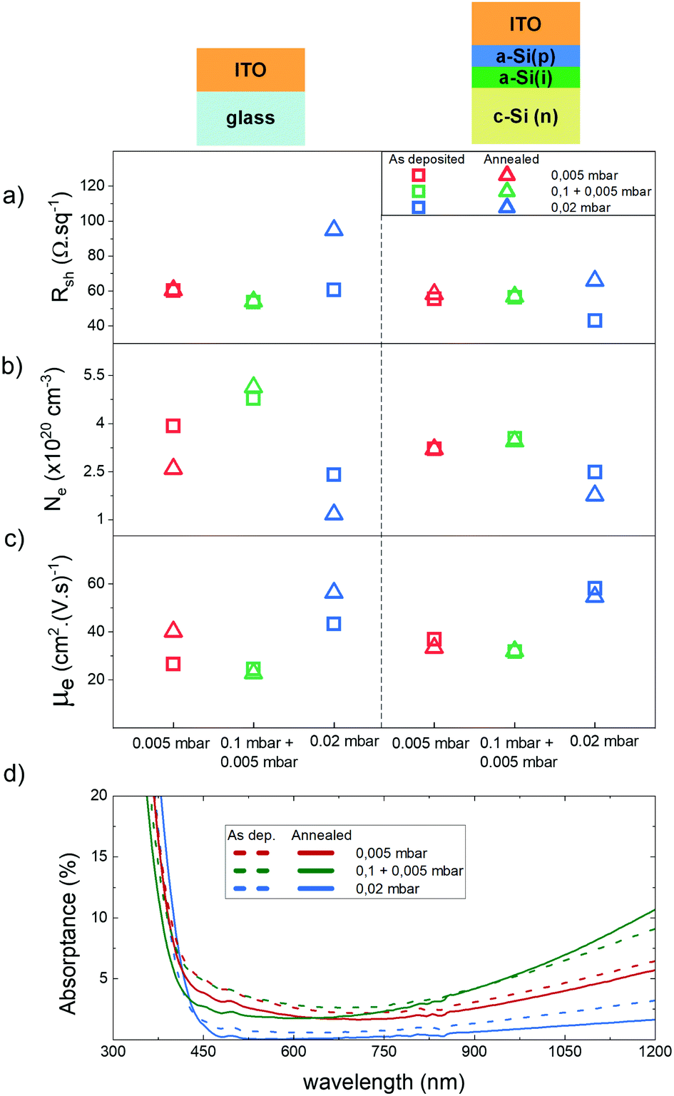 | ||
| Fig. 2 (a) Sheet resistance (Rsh), (b) free carrier density (Ne) and (c) electron mobility (μe) of PLD ITO films deposited at LP (0.005 mbar); LP with buffer (0.1 + 0.005 mbar) and high pressure (0.02 mbar) on glass (left) and a-Si:H/c-Si stacks (right). (d) Absorptance as a function of wavelength of the ITO films. | ||
After the 200 °C annealing step, μe and Ne of all PLD ITO deposited onto the a-Si:H(p/i)/c-Si stacks ITO remain virtually unchanged. Interestingly, similar trends are observed for the LP and LP with buffer ITO on glass, whereas the HP (0.02 mbar) ITO show variations in the properties after annealing. Rsh increases from 60 to 95 Ω □−1 after the heat treatment on glass due to the drop of Ne (from 2.4 to 1.2 × 1020 cm−3). It is important to mention that the reported values represent an average of at least 2 glass samples which have been co-deposited with a SHJ cell stack. The electrical properties of the TCO layers have been previously shown to be dependent on the underlying substrate and to be sensitive towards hydrogen effusion from the hydrogenated a-Si:H layers beneath,19,20 however, this was not observed in our Hall effect measurements on the a-Si:H(p/i)/c-Si(n) stacks. Although this stack seems to be more representative of the device performance, we underline that the developed ITO electrodes were implemented in SHJ cells with a rear emitter design. Therefore, the front current collection would occur from a-Si:H(n/i)/c-Si(n) stack which cannot be reliably measured via the Hall effect due to substantial conduction through the Si substrate in this case.
Optical properties, as shown by the absorptance in Fig. 2(d) and transmittance in Fig. S2 (ESI†), followed the expected trend: a blue shift in the UV due to the Burstein–Moss effect21,22 and increased free carrier absorption (FCA) in the NIR with increased Ne. The lowest FCA and the narrowest optical band gap are observed for the HP film (lowest Ne, highest μe), whereas the highest FCA and widest optical band gap are measured for the LP with the buffer film (highest Ne, lowest μe).
Interestingly, the use of a high-pressure ITO buffer layer promotes ITO crystallization resulting in films with high Ne. This is opposite to an expected increase in μe with enhanced crystallization as demonstrated in other works.15,23 The high Ne instead of high μe of our ITO films with the highest crystallinity indicates that there is a more complex interplay between oxygen vacancies24, grain boundaries16 and ionized impurity scattering,17 in our films. Finally, the optoelectronic properties of the PLD grown ITO films at the three pressure conditions meet the requirements of a front electrode of the SHJ solar cells and/or a rear electrode in ST-PSC, i.e. Rsh < 100 Ω □−1 and low FCA (absorptance below 10% in the spectral range from UV to NIR).25,26 In the following section, the performance of these PLD ITO films on devices will be compared to a sputtered ITO reference for SHJ cells (Rsh ∼ 100 Ω □−1 on textured substrate; Ne ∼ 1.5 × 1020 cm−3, μe ∼ 40 cm2 V−1 s−1) or an opaque Ag electrode for the case of ST-PSC.
2.2 Effect of PLD ITO deposition pressure on buffer-free semi-transparent perovskite solar cells
Sputtered damage during the rear electrode TCO deposition in ST-PSC has been commonly mitigated by the use of an additional evaporated or atomic layer deposited metal oxide buffer layer.6,27 Recently, Zr-doped In2O3 (IZrO) fabricated by PLD at 0.02 mbar allowed damage-free deposition atop of the buffer-free solution-processed ST-PSC due to high (as compared to magnetron sputtering) deposition pressure.11 To verify the effect of PLD pressure during transparent electrode deposition on the damage to the thin (<35 nm) organic electron transport layer, we fabricated semi-transparent vapor-deposited perovskite solar cells without a metal oxide buffer layer and applied the ITO electrodes at the three developed conditions. The cell stack (displayed in the inset of Fig. 3(b)) consisted of glass/ITO (160 nm)/MoO3 (6 nm)/TaTm (10 nm)/MAPbI3 (500 nm)/C60 (25 nm)/BCP (7 nm)/PLD ITO, where TaTm is N4,N4,N4′,N4′-tetra([1,1′-biphenyl]-4-yl)-[1,1′:4′,1′-terphenyl]-4,4′-diamine, C60 is fullerene, and BCP is bathocuproine.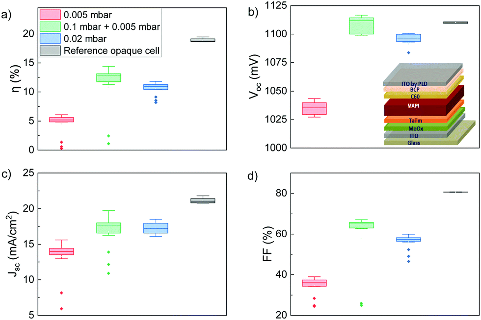 | ||
| Fig. 3 Statistical distribution of the solar cell parameters for semi-transparent perovskite devices with the different PLD ITO deposition pressure conditions. (a) Power conversion efficiency, (b) open-circuit voltage (Voc), (c) short-circuit density (Jsc), and (d) fill factor (FF). Deposition pressure for PLD ITO is indicated in the inset of the graphs. Reference opaque cells with the evaporated Ag rear electrode are shown in grey. | ||
Fig. 3 displays the statistical distribution of the main solar cell parameters for devices with different rear ITO electrodes for the forward scan directions measured from the glass side (forward and reversed scan are presented in Fig. S3, ESI†). The results show clear improvements in open-circuit voltage (Voc) and fill factor (FF) with the increase in the deposition pressure of ITO. Cells with LP ITO show a severe drop in Voc and fill factor (FF) as compared to the opaque reference cell with evaporated Ag back contact. Of note, the thin layer deposited at 0.1 mbar for the case of LP with buffer ITO leads to significant improvements in power conversion efficiency (due to enhanced FF and Voc) as compared to cells with LP ITO. Devices with HP and LP with buffer ITO show comparable short-circuit density (Jsc), yet the FF and Voc are higher for the latter, thus leading to gains in PCE. Nevertheless, cells with HP ITO show only a small drop of Voc and FF with respect to the best performing ST-PSC indicative of a good interface formation for the two conditions. The HP ITO results are in agreement with previous reports for solution-processed ST-PSC with PLD IZrO.11 For the cells with LP ITO, an increased barrier height at the ETL/TCO interface may be causing the severe drop of FF and Voc as suggested by Kanda et al.28 Another possible explanation of the deteriorated cell performance is the penetration of the energetic ablated particles in the organic layer29 due to the suppressed thermalization during PLD at low pressures. The PCE of the reference opaque cell is >19% for the champion cell highlighting the high quality of the halide absorber and relevant choice of the transport layers. Overall, the higher Jsc of the reference cell is related to Ag acting as a back reflector in the cells. Following the confirmation of the effect of increasing the ITO deposition pressure on the damage mitigation of the thin organic transport layers in ST-PSCs, we proceeded to study the effect on SHJ cells.
2.3 Effect of PLD ITO deposition pressure on a-Si:H passivation
In SHJ solar cells, quantitative insights of the induced degradation of the a-Si:H/c-Si interface passivation during TCO deposition are obtained via effective minority carrier lifetime (τeff) measurements. We consistently measured τeff within the passivated c-Si wafer at a fixed minority charge carrier density of 1015 cm−3 on the SHJ cell precursors (shown in the inset of Fig. 4 before ITO deposition (PLD or sputtering)), afterwards and subsequent to the annealing step at 200 °C. Please note that the front-side a-Si:H(n)/a-Si:H(i) stack was slightly thinner (9/8 nm, respectively) as compared to the one in the finished devices (14/10 nm) as described in Section 3.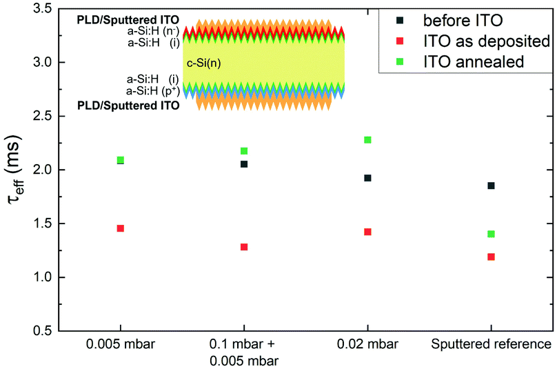 | ||
| Fig. 4 Minority carrier lifetimes before (black squares) and after (red squares) ITO fabrication by PLD at different deposition pressures or reference sputtering process and subsequent to annealing (green squares). | ||
As seen from Fig. 4, a similar drop of τeff from 2 ms to around 1.5 ms is observed for all PLD conditions. Interestingly, the sputtered reference is already deposited at 200 °C which is beneficial for in situ curing of the sputter-induced damage. Nevertheless, we observe the drop of τeff for the case of sputtered ITO as well. As expected, the annealing step at 200 °C recovers the passivation for cell precursors with all transparent electrodes due to the possibility for the a-Si:H network to recover at such elevated temperatures.4,5,30,31 The τeff matches or even slightly exceeds the initial values of a-Si:H coated c-Si wafers (>2 ms) for the case of the HP PLD ITO, whereas the passivation is only slightly improved (1.4 ms vs. 1.2 ms) for the case of sputtered ITO.
2.4 Effect of PLD ITO deposition pressure on SHJ cell performance
Following the lifetime evaluation, the ITO films have been implemented as the front and rear electrodes in SHJ solar cells. The solar cell parameters for the devices with PLD ITO, as well as the reference sputtered ITO, are summarized in Fig. 5. As explained in the experimental section and observed in Fig. 5(f), the wafer contains 7 cells with different Ag grid values (1 and 1.7 mm, respectively). Unless specified separately, we report the solar cell parameters for the devices with 1.7 mm pitch due to the optimized performance.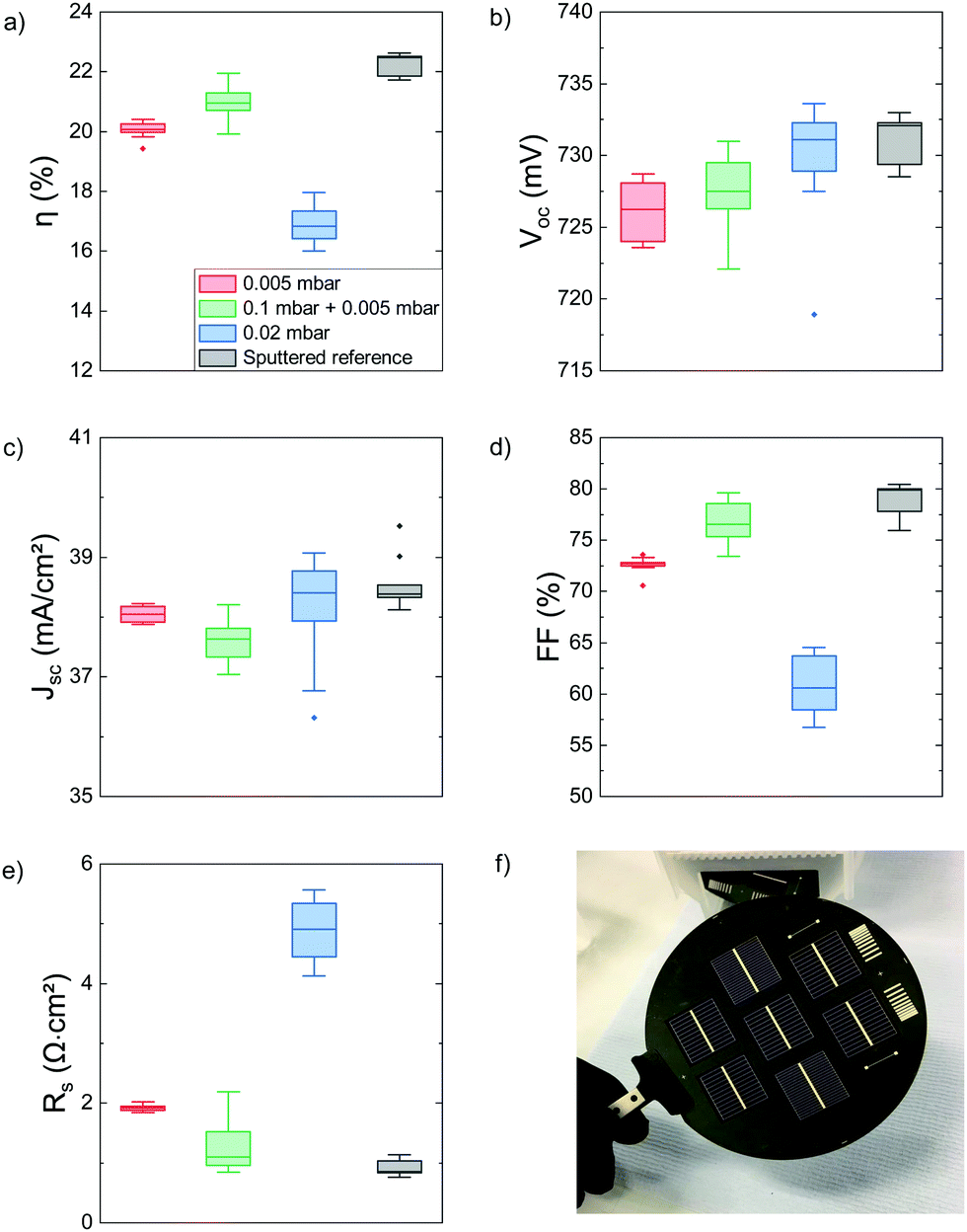 | ||
| Fig. 5 Statistical distribution of silicon heterojunction solar cell parameters measured for the devices with the different PLD ITO deposition conditions. (a) Power conversion efficiency, (b) open-circuit voltage (Voc), (c) short-circuit density (Jsc), (d) fill factor (FF), and (e) series resistance (Rs). Deposition pressure for PLD ITO indicated in the inset of the graphs. Reference cells with sputtered ITO is shown in grey. (f) Image of a 4′′ silicon wafer with 7 finished silicon heterojunction cells (4 cm2) with PLD ITO. | ||
Remarkably, the cells with LP with buffer ITO demonstrate the highest efficiency among the ITO PLD devices (average across the 10 cells) of 21%, but lag behind the established reference cells with sputtered ITO by ∼1.2% as displayed in Fig. 5(a). Devices with LP and HP ITO reach average efficiencies of 20% and 16.9%, respectively. As seen from Fig. 5(b and c), the cells with various ITO electrodes display similar Voc values. Slight differences in Jsc follow the trend observed in Section 2.1 being inversely proportional to the ITO absorptance.
The differences in the overall efficiency originate from the variations in FF for the case of PLD ITO. These changes are mainly dominated by the trend observed in the series resistance (Rs) of the different PLD films. As shown in Fig. 5(e), cells with HP ITO display the most significant increase of Rs (4.9 Ω cm−2), while Rs for the cells with LP with buffer ITO is just a bit higher (1.1 Ω cm−2) than for cells with sputtered ITO (0.86 Ω cm−2). Interestingly, devices with LP ITO display Rs of 1.9 Ω cm−2 which is notably higher than the cells with LP with buffer ITO. This confirms the importance of the thin buffer layer deposited at 0.1 mbar defining the structural and optoelectrical properties of the ITO film. These films have the highest Ne among the PLD ITO films and additionally display the highest crystallinity which may influence the ITO work function at the interface.32,33 Conversely, the highest Rs is observed for cells with the PLD ITO with the lowest Ne. It has been previously shown34,35 that the combination of Ne in TCO films and the activation energy of the a-Si:H films plays a significant role in increasing the contact resistivity (ρc) of the TCO/a-Si:H stack. However, we believe that the difference of ∼2 Ω cm−2 in ρc cannot be accounted for by the rather insignificant difference in Ne (1.5 × 1020 cm−3vs. 3.0 × 1020 cm−3 as measured on planar a-Si:H-coated Si wafers). For these Ne, the expected difference in ρc is in the orders of few tens of mΩ cm−2 as calculated by Luderer et al.36 Therefore, a more plausible contribution to the high Rs could be the potential formation of an amorphous silicon oxide layer at the a-Si:H/ITO interface during PLD which is performed at elevated oxygen partial pressures compared to sputtering. This parasitic oxide may hinder the carrier transport and lead to the increased contact resistance3 which is investigated in the next section.
2.5 Parasitic oxide at the a-Si:H/TCO interface as the source of high series resistance
As mentioned above, the inferior performance of the cells with PLD ITO, as compared to the reference cells with sputtered ITO, is due to the loss of FF because of the compromised Rs. Since the device stacks (c-Si wafer, intrinsic and doped a-Si:H layers and Ag grid) were identical throughout the fabrication process, and considering the similar Rsh of the PLD and sputtered ITO (60 Ω □−1 measured on the a-Si:H/c-Si, Fig. 2(a)), the resistive loss is likely to originate from the ρc at the doped a-Si:H/TCO interface. In particular, the ρc of a-Si(p)/ITO has been previously shown to have the highest contribution to Rs.2,3 Moreover, the ρc of doped a-Si:H/ITO is known to be very sensitive to the oxygen partial pressure during the ITO sputtering process. The process window in sputtering has been shown to be quite narrow, since the working atmosphere during sputtering primarily consists of Ar, whereas minor changes in O2 content (by a few %) lead to the enhancement of ρc36 and severe deterioration of FF.3 This has been explained by the high work function of ITO sputtered at elevated oxygen partial pressures (p(O2)) that increases the barrier height of the a-Si:H/TCO interface.37 The PLD in this study was operated at a much higher oxygen supply and often pure oxygen in the background environment to enable optimized optoelectrical properties. Even for the LP ITO, the p(O2) = 0.005 mbar, whereas for HP ITO the p(O2) = 0.01 mbar, both significantly higher than the p(O2) for sputter processes.7,38 This may lead to the oxidation of a-Si:H layers (intuitively, more likely for HP ITO) suppressing the carrier extraction at the doped a-Si:H/TCO interface. Additionally, a thin native oxide layer can remain in the case of the delayed ITO deposition after the PECVD of the a-Si:H layers. The presence of native oxide typically does not increase the resistive losses as the (rather) high kinetic energy of the sputtered species is sufficient to break the thin SiOx layer. However, that may not be the case of softer PLD due to the different plasma kinetics and requires further studies. In order to decouple the possible causes of increased Rs, a set of solar cells with an HF dip right before the HP ITO PLD deposition was prepared to eliminate the presence of the native oxide. As observed in Fig. 6, no drastic improvement in Rs is present on the device level which suggests that the parasitic oxide is being formed during the deposition. The spread of the values is decreased which may be coincidental due to the smaller sample selection for this experiment. Moreover, comparison of Rs for the co-fabricated cells with different Ag grid pitches reveals minor changes of Rs for an Ag finger spacing of 1 mm vs. 1.7 mm for the case of HP ITO by PLD. This supports the assumption about the minor effect of ITO Rsh on the cell Rs with PLD ITO and dominant contribution of ρc between doped a-Si:H/TCO.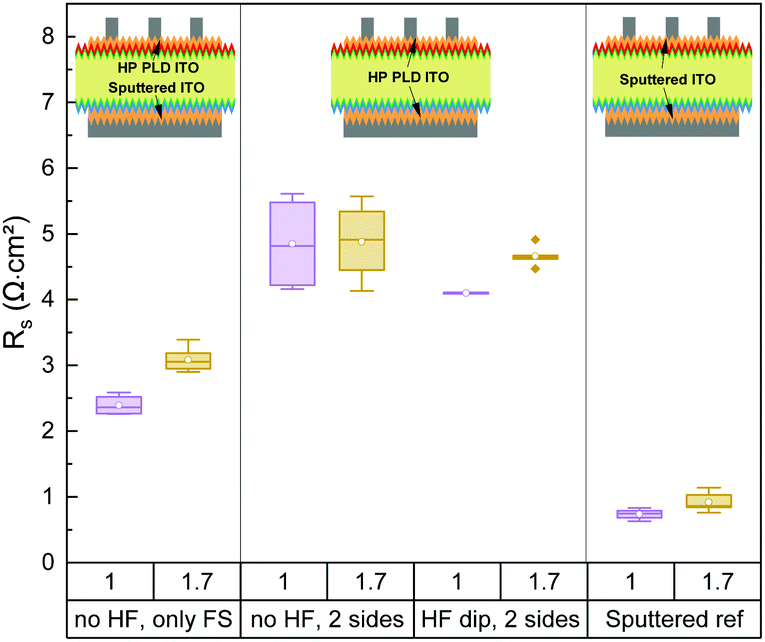 | ||
| Fig. 6 Comparison of total series resistance (Rs) for a set of SHJ cells with PLD ITO at the front and PLD or sputtered rear electrode and Ag grid pitch of 1 and 1.7 mm, respectively. Rs of the cell with double-sided sputtered ITO is given for reference. | ||
To further verify this hypothesis, a batch of SHJ cells with only the front electrode grown via PLD was fabricated (the rear ITO was deposited by sputtering). As seen in Fig. 6, Rs drops substantially by ∼2.5 Ω cm−2 (2.4 vs. 4.9 Ω cm−2). Considering that no lateral transport is needed for the rear contact, this value can be considered as an upper bound for the contribution from the vertical transport, i.e. a good estimation for the ρc of the hole contact stack in the presence of HP ITO. The remaining difference of 1.6 Ω cm−2 in Rs between the double-sided sputtered reference (0.8 Ω cm−2) and only front HP ITO provides, in its turn, an estimation for the ρc of the electron contact stack with HP ITO. These values are high for contacts for SHJ cells but match reasonably well for the case of parasitic oxide hindering the transport of other passivating contacts, such as the TCO/poly-Si contact.3
Chemical mapping of the ITO/a-Si:H(i/n) interface was furthermore performed via time-of-flight secondary ion mass spectrometry (ToF-SIMS) and high-resolution energy dispersive X-ray spectroscopy (EDX) under a scanning transmission electron microscope (STEM). Fig. 7(a and b) show the ToF-SIMS depth profile resulting from ablation using a Cs+ source from the HP ITO towards the c-Si both before and after annealing. It should be noted that the annealed states resemble the situation in the solar cell for which JV measurements have been performed after annealing at 200 °C. One measurement frame was performed after every ablation while tracking In2O3−, Si−, H− (Fig. 7(a)) and SiHO2−/SiO3In− (Fig. 7(b)) signals, respectively, with a quadrupole mass spectrometer. SIMS measurement data for LP ITO and HP ITO are presented in Fig. S4 (ESI†). Si− and In2O3− signals do not change upon annealing for any samples and therefore allow identification of the ITO/a-Si:H interface. H− is observed for all samples before and after annealing suggesting the presence of H− in ITO already in the as-deposited state. In contrast to what has been shown by Cruz et al.20 or Ritzau et al.,39 we do not observe additional H− diffusion into the ITO layer from the a-Si:H. This agrees with the Hall effect data, showing that Ne does not change upon annealing of the ITO/a-Si:H planar stacks. SIMS measurements also allowed detection of SiO3In− and SiHO2− signals which are indicative of oxygen presence. Fig. 7(b) and Fig. S4 (ESI†) show that the SiO3In− and SiHO2− signals are only present in the vicinity of the TCO/a-Si:H interface, both before and after annealing. The high intensity of the SiHO2− signal at the TCO/a-Si:H interface indicates the oxidation of the a-Si:H surface during ITO deposition. In order to compare the SiOx layer for the three PLD conditions, before and after annealing, SiO3In− and SiHO2− signals were extracted and plotted independently for each sample in Fig. 7(c and d). The full width at half maximum (FWHM) and the area of these two signals were measured before and after annealing and are reported in Table S1 (ESI†). The results indicate that the SiOx layer is present for all as-deposited samples with a similar thickness independent of the PLD deposition pressure.
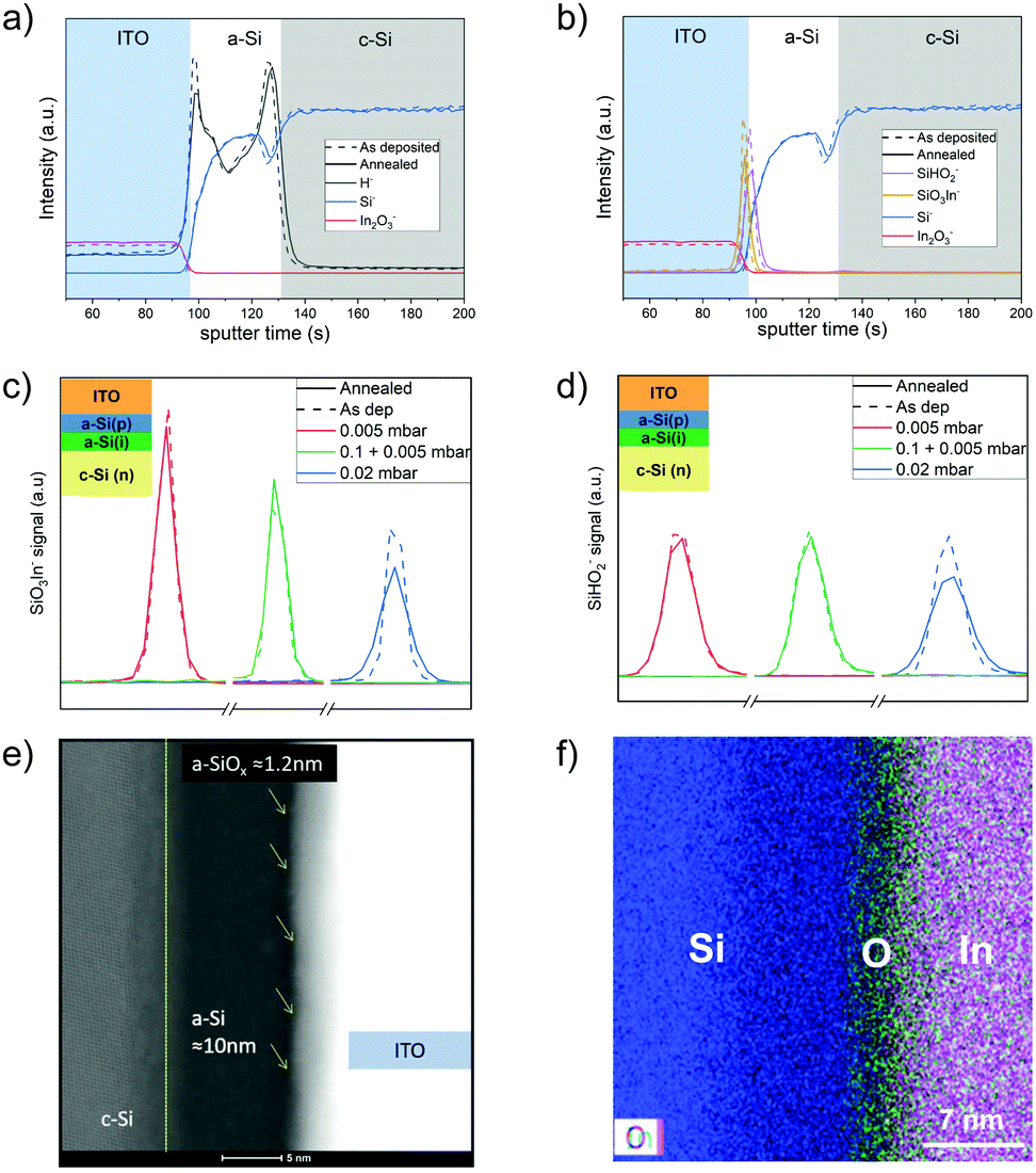 | ||
| Fig. 7 Cross-sectional ToF-SIMS analysis of HP ITO on the SHJ solar cell stack before and after annealing. (a) H− signal; (b) SiHO2− and SiO3In− signals. Signals plotted next to Si−, In2O3− signals to define the ITO/a-Si:H interface. Integrated ToF-SIMS intensity profiles for (c) SiHO2− and (d) SiO3In− signals indicative of oxygen presence. HRSTEM-HAADF analysis of the finished SHJ solar cells with HP ITO after metallization: (e) image of the a-Si:H/ITO interface; (f) energy dispersive X-ray chemical mapping of a chosen area within the sample where blue, green and pink represents silicon, oxygen and indium, respectively. | ||
For both the SiHO2− and SiO3In− signals, the only significant change in FWHM is observed for the stack with HP ITO, showing broadening of the peak after annealing. This suggests possible oxygen migration at the ITO/a-Si:H interface, increasing the SiOx barrier width after annealing. We observe this only for the HP ITO sample, which is the amorphous film before and after annealing. The density of the film or even its possible higher oxygen content (due to higher p(O2) during the deposition process) might be the cause of this effect. The observation also agrees with the higher Rs for the SHJ cells with the HP as ITO reported in Section 2.1. The ToF-SIMS measurements, the same as the Hall effect measurements, were all performed in the ITO/a-Si:H(n/i)/c-Si planar stacks. To verify the presence of the SiOx also on the cells analyzed in Fig. 5 (textured wafers instead of planar), scanning transmission electron microscope high-angle annular dark field (STEM-HAADF) EDX was performed on FIB prepared lamellas taken directly from the cells. The contrast in STEM imaging of the amorphous layers next to the HP ITO films in Fig. 7(e) suggests the presence of ∼1.2 nm a-SiOx next to the a-Si:H thin film. The EDX chemical mapping corresponding to the zoomed area (Fig. 7(f)) indicates the oxygen (green) signal between the indium (pink) and silicon (blue) layers. Identical analysis for the LP ITO and LP ITO with the buffer is displayed in Fig. S5 (ESI†). The increase in the O− signal prior to indium and tin signals is clearly observed for all ITO samples in the STEM-HAADF EDX line scan profile recorded across the a-Si:H/ITO interface (as shown in Fig. S5(g–i), ESI†). Interestingly, the a-SiOx layer is present for cells with ITO by PLD as confirmed by both STEM and ToF-SIMS measurements. The absence of hydrogen effusion into the ITO layers observed by ToF-SIMS may suggest that the thin a-SiOx also acts as the hydrogen blocking layer. However, the presence of this a-SiOx thin layer only leads to severe degradation of FF for cells with HP ITO. This may also be indicative of a thicker/denser parasitic oxide layer for the case of HP ITO.3 Nevertheless, distinguishing a minor difference in the thicknesses of the SiOx for each of the pressure conditions from the local EDX/TEM measurements is challenging and cannot be easily decoupled from other effects such as the crystallinity of the ITO layers and/or its Ne as discussed in Section 2.4.
2.6 High efficiency SHJ cells with thinner ITO by PLD
Due to the scarcity and high price of indium,40 it is desirable to decrease the thickness of the ITO electrodes in the solar cells. The sufficient conductivity of ITO in the PLD process enabled thinning down the transparent electrode to 45 nm (on textured wafer) maintaining the desired Rsh < 100 Ω □−1. However, for a given refractive index of the front electrode (n ∼ 2 in the visible), a total thickness of ∼75 nm on textured wafers is required to meet the anti-reflective coating (ARC) conditions with a reflection minimum at 600 nm. Therefore, the difference in the thickness should be compensated by another layer on top of the thinner ITO electrode. Spray-casted TiOx (∼50 nm on textured wafer) was utilized for these purposes due to its matching refractive index41 and the cost-effectiveness of the deposition process. Cells with thinner LP with buffer ITO (and TiOx capping layer) as the front electrode and the rear sputtered ITO were used for this demonstration. The box plots of the SHJ solar cell parameters after TiOx deposition are displayed in Fig. 8. As expected, the Jsc is improved by 1 mA cm−2 (38.1 vs. 37.1), while Voc remained on the same level (733 mV). Additionally, a small gain of 0.7% in FF (79.4% vs. 78.7%) related to the decreased Rs (1.02 vs. 1.19 Ω cm−2) which may be caused by a short (∼10 minutes) additional heat treatment during the TiOx deposition which is performed at 200 °C. All in all, the cells demonstrated an overall increase in the efficiency of 0.8% (22.0% vs. 21.2%) by adding the TiOx capping. This proves that thinning down of the PLD ITO electrodes together with depositing the TiOx capping layer is a promising strategy to fabricate high-performing SHJ cells with decreased indium consumption. | ||
| Fig. 8 Statistical distribution of solar cell parameters measured for the devices with the different PLD ITO deposition conditions. (a) Power conversion efficiency, (b) open-circuit voltage (Voc), (c) short-circuit density (Jsc), (d) fill factor (FF), and (e) series resistance (Rs). Cross-section of the silicon heterojunction cell (SHJ) with a thin ITO and TiOx capping layer. | ||
3. Experimental
ITO films were grown by Pulsed Laser Deposition (wafer-based System from Solmates BV) from a 98/2 wt% In2O3/SnO2 target at room temperature at the University of Twente.42 All experiments were performed using a KrF (λ = 248 nm) Compex-pro laser (COHERENT) with a pulse repetition rate of 10 Hz and a fluence of 2.6 J cm−2. ITO was co-deposited on glass substrates (EcoGlass SCHOTT) and textured or planar a-Si:H(n)/a-Si:H(i)/c-Si/a-Si:H(i)/a-Si:H(p) substrates for different characterizations. Glass substrates were ultrasonicated in acetone and isopropanol for 5 minutes and rinsed in deionized water prior to deposition. Three different PLD pressure conditions were developed to obtain ITO with an Rsh of 60 Ω □−1 in the as-deposited state for ∼100 nm thick films on planar substrates. Deposition pressure conditions: 0.005 mbar (100% O2 background gas), 0.02 mbar (50/50% Ar/O2) and the third condition consisted of a very thin ITO layer (about 2 nm thick) deposited at 0.1 mbar (100% O2) followed by a thicker ITO deposited at 0.005 mbar. The background gas flow was kept constant while the deposition pressure was controlled by the position of the butterfly valve between the turbomolecular pump and the vacuum chamber. Post-annealing of the ITO was performed at 200 °C in air for 20 minutes.Optical properties of the ITO films were measured on a UV-Vis-NIR spectrophotometer PerkinElmer Lambda 950S using an integrating sphere. Absorptance (A), defined as A = 1 − TT − TR, where TT is the total transmittance and TR is the total reflectance, of the films on glass. Sheet resistance (Rsh), free carrier density (Ne) and electron Hall mobility (μe) were determined using a Hall Effect measurement setup in the van der Pauw configuration, using 1 × 1 cm2 pre-diced samples. The structural properties of the films were investigated using an Xpert Pro diffractometer (Panalytical) in grazing incidence (GI-XRD) configuration were the incident angle is ω = 0.6°. The ITO thickness was determined by measuring the step height on glass samples with a Dektak stylus profilometer. Time-of-flight secondary ion mass spectrometry (ToF-SIMS) was performed by TESCAN analytics. Ablation was done using a Cs+ source on a 200 μm2 area. The process was performed such that one measurement frame was performed after every ablation frame while tracking H−/In2O3−/Si−/SiHO2− and SiO3In− signals with a quadrupole mass spectrometer.
Chemical analyses were performed in the scanning transmission electron microscope high-angle annular dark field (STEM-HAADF) imaging mode of a 200 kV Titan-Themis TEM/STEM electron microscope equipped with a Cs probe corrector and a ChemiSTEM Super-X detector. Prior to the analysis, the FIB technique was used for the preparation of cross-section lamellas of the considered sample. STEM-HAADF EDX chemical mapping was performed by considering the following elements of interest: the silicon Kα-1.73 keV ionization present in the substrate, the a-SiOx layer and the a-Si:H layer, the oxygen Kα-0.523 keV ionization edge coming also from the thermal a-SiOx and the indium L-3.28 keV ionization edge from the ITO layer.
Solar cells and lifetime test structures were fabricated on random pyramid textured 1 Ω cm, and 180 μm thick n-type FZ silicon wafers at Fraunhofer ISE. The monofacial solar cells were fabricated in the rear-emitter design and metallized at the front and rear side via screen printing of an Ag paste cured at 200 °C in a belt furnace. The a-Si:H layers are deposited by plasma-enhanced chemical vapor deposition (PECVD) using mixtures of SiH4, H2, TMB, and PH3. These precursors were later shipped to the University of Twente for PLD ITO. The reference ITO samples were deposited inline via DC magnetron sputtering from a rotary 97/3 wt% In2O3/SnO2 target with a deposition substrate temperature of 190 °C. The power of 4.4 kW was distributed along the 75 cm long target, and the deposition pressure was kept at 4 × 10⁻³ mbar in 5% O2 in an Ar atmosphere.
Semi-transparent perovskite solar cells (ST-PSC) were fabricated by thermal evaporation in vacuum chambers at 10−6 mbar, which are integrated in a nitrogen-filled glovebox (H2O and O2 < 0.1 ppm) at the University of Valencia. The vacuum chambers are equipped with temperature-controlled evaporation sources (Creaphys) fitted with ceramic crucibles, directed upward. Individual quartz crystal microbalance (QCM) sensors monitored the deposition rate of each evaporation source. As mentioned in Section 2.2, the evaporated perovskite solar cell stack consisted of glass/ITO (160 nm)/MoO3 (6 nm)/TaTm (10 nm)/MAPbI3 (500 nm)/C60 (25 nm)/BCP (7 nm). The deposition of the perovskite and charge transport layers followed the same procedure described in our previous publications.43,44 The ST-PSC substrates were later shipped to the University of Twente for rear transparent ITO electrode fabrication by PLD. For the ITO PLD deposition, the substrates were aligned to shadow masks to obtain the electrode layout indicated in Fig. S6 (ESI†) with sixteen rectangular pixels of 0.0825 cm2, eight on each side of the substrate, allowing for significant statistics. No silver grid lines surrounding the PLD-ITO contacts were used for semi-transparent cells in this study. An Ag grid for the reference opaque cells was fabricated by thermal evaporation at the University of Valencia.
4. Conclusions
We demonstrated ITO films at various deposition pressures with good optoelectrical properties by wafer-scale PLD at room temperature. PLD ITO fabricated at elevated pressures leads to the improvement in FF and Voc for the semi-transparent perovskite solar cells suggesting the reduced damage at the transport layer/TCO interface. In contrast, no difference in passivation quality and, consequently, Voc was observed for silicon heterojunction cells with different ITO electrodes, whereas increased PLD pressures lead to a high series resistance and deterioration in FF. The optimized crystalline ITO films enable sufficient transport across the a-Si:H/ITO interface despite the presence of a thin a-SiOx as revealed by ToF-SIMS and STEM. We implemented ITO by PLD in silicon heterojunction cells to obtain high efficiencies of 21%. Finally, we demonstrated that thinning down the PLD ITO electrodes together with depositing a TiOx capping layer is a feasible strategy to fabricate high-performing devices with efficiencies >22% and a reduction in indium consumption. This study draws attention toward the common issue for ‘soft landing’ TCO deposition techniques utilizing a high process pressure with PLD serving as a case study. Our findings motivate further research activities in order to benefit from low-damage TCO deposition without compromising the contact resistance with adjacent transport layers in optoelectronic devices.Author contributions
Y. S. and P.-A. R. share equal contributions for conceiving the idea and ITO characterization. P.-A. R. conducted ITO optimization by PLD, optoelectrical characterization and processed devices. Y. S. performed structural characterization of ITO, data visualization and solar cell analysis. L. T. fabricated and characterized silicon heterojunction solar cells and conducted lifetime measurements, I. F. performed HRSTEM-HAADF and EDX measurements and analysis, K. Z. and A. P. fabricated and characterized the perovskite solar cells. Y. S., P.-A. R. and M. M.-M. drafted the manuscript. All co-authors discussed the paper and revised the manuscript. H. B., P. C., M. B. and M. M.-M. were involved in designing the experiments and supervised the work.Conflicts of interest
There are no conflicts to declare.Acknowledgements
This work was partly supported by the Solar-ERA.NET CUSTCO project by the Netherlands Enterprise Agency (RVO) under contract SOL18001, the French Research National Agency (ANR) under contract ANR-19-SOL2-0002-04, and the German Federal Ministry for Economic Affairs and Energy under Contract 03EE1032. FIB lamella sample preparation and STEM-HAADF EDX characterizations were performed in the frame of the French Government program of investment for the future (Programme d'Investissement d'Avenir—TEMPOS Equipex—ANR-10-EQPX-50, pole NanoTEM). H. J. B. acknowledges the financial support from Project PCI2019-111829-2 funded by MCIN/AEI/10.13039/501100011033 and by the European Union, Project CEX2019-000919-M funded by MCIN/AEI/10.13039/501100011033, and the Comunitat Valenciana (IDIFEDER/2018/061 and Prometeu/2020/077). H. J. B. also acknowledges financial support by the King Abdullah University of Science and Technology (KAUST) Office of Sponsored Research (OSR) under award numbers OSR-2019-CARF/CCF-3097 and OSR-2019-CRG-4093. K. P. S. Z. acknowledges funding from Comunitat Valenciana (APOSTD/2021/368). A. P. acknowledges his Grisolia grant from the Comunitat Valenciana (GRISOLIAP/2020/134).References
- E. Aydin, M. De Bastiani and S. De Wolf, Adv. Mater., 2019, 31, 1900428 CrossRef PubMed.
- M. A. Leilaeioun, W. Weigand, M. Boccard, Z. J. Yu, K. Fisher and Z. C. Holman, IEEE J. Photovolt., 2020, 10, 54–62 Search PubMed.
- C. Messmer, M. Bivour, C. Luderer, L. Tutsch, J. Schön, M. Hermle, J. Schon and M. Hermle, IEEE J. Photovolt., 2020, 10, 343–350 Search PubMed.
- B.-M. Meiners, D. Borchert, S. Hohage, S. Holinksi and P. Schäfer, Phys. Status Solidi A, 2015, 212, 1817–1822 CrossRef CAS.
- B. Demaurex, S. De Wolf, A. Descoeudres, Z. Charles Holman and C. Ballif, Appl. Phys. Lett., 2012, 101, 171604 CrossRef.
- E. Aydin, C. Altinkaya, Y. Smirnov, M. A. Yaqin, K. P. Zanoni, A. Paliwal, Y. Firdaus, T. G. Allen, T. D. Anthopoulos, H. J. Bolink, M. Morales-Masis and S. De Wolf, Matter, 2021, 4, 3549–3584 CrossRef CAS.
- L. Tutsch, M. Bivour, W. Wolke, M. Hermle and J. Rentsch, Proceedings of the 33rd European PV Solar Energy Conference and Exhibition, 2017, pp. 24–29 Search PubMed.
- A. J. Bett, K. M. Winkler, M. Bivour, L. Cojocaru, O. S. Kabakli, P. S. C. Schulze, G. Siefer, L. Tutsch, M. Hermle and S. W. Glunz, et al. , ACS Appl. Mater. Interfaces, 2019, 11, 45796–45804 CrossRef CAS PubMed.
- S. Schubert, F. Schmidt, H. von Wenckstern, M. Grundmann, K. Leo and L. Müller-Meskamp, Adv. Funct. Mater., 2015, 25, 4321–4327 CrossRef CAS.
- J. M. Dekkers and J. A. Janssens, Method for depositing a target material onto a organic electrically functional material, WO Patent 060356, 2014 Search PubMed.
- Y. Smirnov, L. Schmengler, R. Kuik, P.-A. Repecaud, M. Najafi, D. Zhang, M. Theelen, E. Aydin, S. Veenstra and S. De Wolf, et al. , Adv. Mater. Technol., 2021, 6, 2000856 CrossRef CAS.
- P. Willmott, Prog. Surf. Sci., 2004, 76, 163–217 CrossRef CAS.
- M. Marezio, Acta Crystallogr., 1966, 20, 723–728 CrossRef CAS.
- D. C. Paine, T. Whitson, D. Janiac, R. Beresford, C. O. Yang and B. Lewis, J. Appl. Phys., 1999, 85, 8445 CrossRef CAS.
- B. Houng, S. L. Lin, S. W. Chen and A. Wang, Ceram. Int., 2011, 37, 3397–3403 CrossRef CAS.
- H. C. Lee and O. O. Park, Vacuum, 2004, 75, 275–282 CrossRef CAS.
- T. Pisarkiewicz, K. Zakrzewska and E. Leja, Thin Solid Films, 1989, 174, 217–223 CrossRef CAS.
- D. Zhang and H. Ma, Appl. Phys. A: Mater. Sci. Process., 1996, 62, 487–492 CrossRef.
- A. Cruz, D. Erfurt, P. Wagner, A. B. Morales-Vilches, F. Ruske, R. Schlatmann and B. Stannowski, Sol. Energy Mater. Sol. Cells, 2021, 236, 111493 CrossRef.
- A. Cruz, R. Schlatmann, B. Stannowski, F. Ruske, A. Eljarrat, P. P. Michalowski, A. B. Morales-Vilches, S. Neubert, E. C. Wang, C. T. Koch and B. Szyszka, IEEE J. Photovoltaics, 2020, 10, 703–709 Search PubMed.
- E. Burstein, Phys. Rev., 1954, 93, 632–633 CrossRef CAS.
- T. S. Moss, Proc. Phys. Soc., London, Sect. B, 1954, 67, 775 CrossRef.
- X. W. Sun, L. D. Wang and H. S. Kwok, Thin Solid Films, 2000, 360, 75–81 CrossRef CAS.
- J. E. Medvedeva, D. B. Buchholz and R. P. H. Chang, Adv. Electron. Mater., 2017, 3, 1700082 CrossRef.
- M. Morales-Masis, S. De Wolf, R. Woods-Robinson, J. W. Ager and C. Ballif, Adv. Electron. Mater., 2017, 3, 1600529 CrossRef.
- Z. C. Holman, A. Descoeudres, L. Barraud, F. Z. Fernandez, J. P. Seif, S. De Wolf and C. Ballif, IEEE J. Photovolt., 2012, 2, 7–15 Search PubMed.
- K. A. Bush, C. D. Bailie, Y. Chen, A. R. Bowring, W. Wang, W. Ma, T. Leijtens, F. Moghadam and M. D. McGehee, Adv. Mater., 2016, 28, 3937–3943 CrossRef CAS PubMed.
- H. Kanda, A. Uzum, A. K. Baranwal, T. A. N. Peiris, T. Umeyama, H. Imahori, H. Segawa, T. Miyasaka and S. Ito, J. Phys. Chem. C, 2016, 120, 28441–28447 CrossRef CAS.
- M. J. Griffith, N. A. Cooling, B. Vaughan, K. M. O'Donnell, M. F. Al-Mudhaffer, A. Al-Ahmad, M. Noori, F. Almyahi, W. J. Belcher and P. C. Dastoor, Energy Technol., 2015, 3, 428–436 CrossRef CAS.
- F. Lebreton, S. Abolmasov, F. Silva and P. Roca i Cabarrocas, Appl. Phys. Lett., 2016, 108, 051603 CrossRef.
- H. Plagwitz, B. Terheiden and R. Brendel, J. Appl. Phys., 2008, 103, 094506 CrossRef.
- M. V. Hohmann, P. Ágoston, A. Wachau, T. J. M. Bayer, J. Brötz, K. Albe and A. Klein, J. Phys.: Condens. Matter, 2011, 23, 334203 CrossRef PubMed.
- A. Tomasi, F. Sahli, J. P. Seif, L. Fanni, S. M. de Nicolas Agut, J. Geissbühler, B. Paviet-Salomon, S. Nicolay, L. Barraud and B. Niesen, et al. , IEEE J. Photovolt., 2015, 6, 17–27 Search PubMed.
- P. Procel, G. Yang, O. Isabella and M. Zeman, Sol. Energy Mater. Sol. Cells, 2018, 186, 66–77 CrossRef CAS.
- P. Procel, H. Xu, A. Saez, C. Ruiz-Tobon, L. Mazzarella, Y. Zhao, C. Han, G. Yang, M. Zeman and O. Isabella, Prog. Photovoltaics, 2020, 28, 935–945 CAS.
- C. Luderer, L. Tutsch, C. Messmer, M. Hermle and M. Bivour, IEEE J. Photovoltaics, 2021, 11, 329–336 Search PubMed.
- F.-J. Haug, R. Biron, G. Kratzer, F. Leresche, J. Besuchet, C. Ballif, M. Dissel, S. Kretschmer, W. Soppe and P. Lippens, et al. , Prog. Photovoltaics, 2012, 20, 727–734 CAS.
- M. Morales-Masis, S. Martin De Nicolas, J. Holovsky, S. De Wolf and C. Ballif, IEEE J. Photovolt., 2015, 5, 1340–1347 Search PubMed.
- K.-U. Ritzau, T. Behrendt, D. Palaferri, M. Bivour and M. Hermle, Thin Solid Films, 2016, 599, 161–165 CrossRef CAS.
- C. Candelise, J. F. Speirs and R. J. K. Gross, Renewable Sustainable Energy Rev., 2011, 15, 4972–4981 CrossRef CAS.
- M. Glatthaar, S. Janz, H. Hauser, B. Bläsi, M. Bivour, S. Kluska, R. Hermann, L. Tutsch, R. Mahmoud Algazzar, L. Jakob, U. Heitmann and J. Bartsch, 37th European Photovoltaic Solar Energy Conference and Exhibition, 2020, pp. 44–47 Search PubMed.
- D. H. Blank, M. Dekkers and G. Rijnders, J. Phys. D: Appl. Phys., 2013, 47, 034006 CrossRef.
- D. Perez-del Rey, L. Gil-Escrig, K. P. Zanoni, C. Dreessen, M. Sessolo, P. P. Boix and H. J. Bolink, Chem. Mater., 2019, 31, 6945–6949 CrossRef CAS.
- A. Babaei, K. P. Zanoni, L. Gil-Escrig, D. Pérez-del Rey, P. P. Boix, M. Sessolo and H. J. Bolink, Front. Chem., 2020, 7, 936 CrossRef PubMed.
Footnotes |
| † Electronic supplementary information (ESI) available. See DOI: 10.1039/d1ma01225h |
| ‡ These authors contributed equally to this work. |
| This journal is © The Royal Society of Chemistry 2022 |